Rectifier and Filter Circuits
Introduction
The circuit elements most vulnerable to failure in any given piece of electronic hardware are those exposed to the outside world. In most systems, the greatest threat generally involves the ac-to-dc power supply. The power supply is subject to high-energy surges from lightning and other sources. Because power-supply systems often are exposed to extreme voltage and environmental stresses, derating of individual components is a key factor in improving supply reliability. The goal of derating is to reduce the electrical, mechanical, thermal, and other environmental stresses on a component to decrease the degradation rate and to prolong useful life. Through derating, the margin of safety between the operating stress level and the maximum permissible stress level for a given part is increased. This consideration provides added protection from system overstress, unforeseen during design.
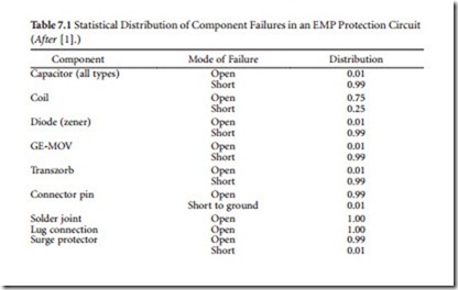
Experience has demonstrated that types of components tend to fail in predictable ways. Table 7.1 shows the statistical distribution of failures for a transient-suppression (EMP) protection circuit. Although the data presented applies only to a specific product, some basic conclusions can be drawn:
• The typical failure mode for a capacitor is a short circuit.
• The typical failure mode for a zener diode is a short circuit.
• The typical failure mode for a connector pin is an open circuit.
• The typical failure mode for a solder joint is an open circuit.
These conclusions present no great surprises, but they point out the predictability of equipment failure modes. The first step in solving a problem is knowing what is likely to fail and what the typical failure modes are.
Power Rectifiers
Virtually all power supplies use silicon rectifiers as the primary ac-to-dc converting device. Rectifier parameters generally are expressed in terms of reverse-voltage ratings and mean-forward-current ratings
in a ∫-wave rectifier circuit operating from a 60 Hz supply and feeding a purely resistive load. The three
primary reverse-voltage ratings are:
• Peak transient reverse voltage (Vrm) — the maximum value of any nonrecurrent surge voltage. This value must never be exceeded.
• Maximum repetitive reverse voltage [Vrm(rep)] — the maximum value of reverse voltage that can be applied recurrently (in every cycle of 60 Hz power). This includes oscillatory voltages that may appear on the sinusoidal supply.
• Working peak reverse voltage [Vrm(wkg)] — the crest value of the sinusoidal voltage of the ac supply at its maximum limit. Rectifier manufacturers generally recommend a value that has a significant safety margin, relative to the peak transient reverse voltage (Vrm), to allow for transient overvoltages on the supply lines.
There are three forward-current ratings of similar importance in the application of silicon rectifiers:
• Nonrecurrent surge current [Ifm(surge)] — the maximum device transient current that must not be exceeded at any time. Ifm(surge) is sometimes given as a single value, but often is presented in the form of a graph of permissible surge-current values vs. time. Because silicon diodes have a relatively small thermal mass, the potential for short-term current overloads must be given careful consideration.
• Repetitive peak forward current [Ifm(rep)] — the maximum value of forward current reached in each cycle of the 60 Hz waveform. This value does not include random peaks caused by transient disturbances.
• Average forward current [Ifm(av)] — the upper limit for average load current through the device. This limit is always well below the repetitive peak forward-current rating to ensure an adequate margin of safety.
Rectifier manufacturers generally supply curves of the instantaneous forward voltage vs. instantaneous forward current at one or more specific operating temperatures. These curves establish the for- ward-mode upper operating parameters of the device.
Figure 7.1 shows a typical rectifier application in a bridge rectifier circuit.
Operating Rectifiers in Series
High-voltage power supplies (5 kV and greater) often require rectifier voltage ratings well beyond those typically available from the semiconductor industry. To meet the requirements of the application, manufacturers commonly use silicon diodes in a series configuration to yield the required working peak reverse voltage. For such a configuration to work properly, the voltage across any one diode must not exceed the
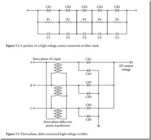
rated peak transient reverse voltage (Vrm) at any time. The dissimilarity commonly found between the reverse leakage current characteristics of different diodes of the same type number makes this objective difficult to achieve. The problem normally is overcome by connecting shunt resistors across each rectifier in the chain, as shown in Figure 7.2. The resistors are chosen so that the current through the shunt elements (when the diodes are reverse-biased) will be several times greater than the leakage current of the diodes themselves.
The carrier storage effect also must be considered in the use of a series-connected rectifier stack. If precautions are not taken, different diode recovery times (caused by the carrier storage phenomenon) will effectively force the full applied reverse voltage across a small number of diodes, or even a single diode. This problem can be prevented by connecting small-value capacitors across each diode in the rec- tifier stack. The capacitors equalize the transient reverse voltages during the carrier storage recovery peri- ods of the individual diodes.
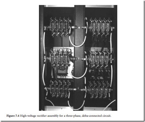
Figure 7.3 illustrates a common circuit configuration for a high-voltage, three-phase rectifier bank. A photograph of a high-voltage, series-connected, three-phase rectifier assembly is shown in Figure 7.4.
Operating Rectifiers in Parallel
Silicon rectifiers are used in a parallel configuration when a large amount of current is required from the power supply. Parallel assemblies normally are found in low-voltage, high-current supplies. Current sharing is the major design problem with a parallel rectifier assembly because diodes of the same type number do not necessarily exhibit the same forward characteristics.
Semiconductor manufacturers often divide production runs of rectifiers into tolerance groups, matching forward characteristics of the various devices. When parallel diodes are used, devices from the same tolerance group must be selected to avoid unequal sharing of the load current. As a margin of safety, designers allow a substantial derating factor for devices in a parallel assembly to ensure that the maxi- mum operating limits of any one component are not exceeded.
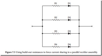
The problems inherent in a parallel rectifier assembly can be reduced through the use of a resistance or reactance in series with each component, as shown in Figure 7.5. The build-out resistances (R1 through R4) force the diodes to share the load current equally. Such assemblies can, however, be difficult to construct and may be more expensive than simply adding diodes or going to higher-rated components. Power loss issues must also be considered with this approach.
Silicon Avalanche Rectifiers
The silicon avalanche diode is a special type of rectifier that can withstand high reverse power dissipation. For example, an avalanche diode with a normal forward rating of 10 A can dissipate a reverse transient of 8 kW for 10 ms without damage. This characteristic of the device allows elimination of the surge-absorption capacitor and voltage-dividing resistor networks needed when conventional silicon diodes are used in a series rectifier assembly. Because fewer diodes are needed for a given applied reverse voltage, significant underrating of the device (to allow for reverse voltage transient peaks) is not required.
When an extra-high-voltage rectifier stack is used, it is still advisable to install shunt capacitors — but not resistors — in an avalanche diode assembly. The capacitors are designed to compensate for the effects of carrier storage and stray capacitance in a long series assembly.
Single-Phase Rectifier Configurations
Rectifiers are one of the building blocks of ac power systems. Diodes are used to form rectifiers in elec- tronic power supplies using one of four basic circuits:
• Half-wave
• Full-wave
• Bridge
• Voltage multiplier
Half-Wave Rectifier
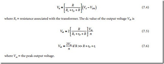
The half-wave rectifier circuit is shown in Figure 7.6a [2]. When the input sinusoid voltage at A goes pos- itive, the diode conducts, resulting in current in the load resistor R. When the input voltage goes negative, the diode becomes reverse-biased and, hence, does not conduct, resulting in negligible current across R. Therefore, the output voltage is given by
The following general aspects must be considered when designing a half-wave diode power supply:
• The current- or power-handling capability of the diode.
• The peak inverse voltage (PIV) that the diode must be able to withstand without breakdown. When the input voltage goes negative, the diode becomes reverse-biased and the input voltage VS appears across the diode.
Full-Wave Rectifier
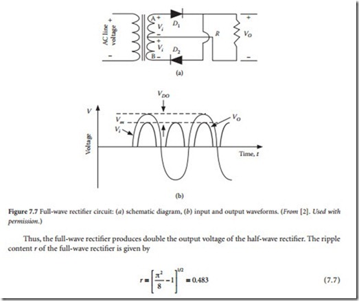
The full-wave rectifier utilizes both halves of the input sinusoid [2]. One common implementation is shown in Figure 7.7a. The full-wave rectifier consists of two half-wave rectifiers connected to a load R. The secondary transformer winding is center tapped to provide two equal voltages Vi for each half-wave rectifier. When the node A is at positive polarity, Vi with respect to node B, D1 will be forward-biased and D2 will be reverse-biased. Therefore, diode D1 will conduct and the current will flow through R back to the center tap of the transformer. When the node B is at positive polarity Vi with respect to node A, D2 will be forward-biased and diode D1 will be reverse-biased. The current conducted by D2 will flow through R and back to center tap. The current through R is always in the same direction, giving rise to unipolar voltage VO across R. The input and output voltage waveforms of the full-wave rectifier are shown in Figure 7.7b.
The output voltage of the full-wave rectifier is given by
The ripple factor for a full-wave rectifier is significantly less than that of a half-wave rectifier.
Another important element to be considered in the design of a full wave rectifier is the peak inverse voltage rating of the diodes. During the positive half-cycle, diode D1 is conducting and D2 is cut off. The voltage at the cathode of D2 will be at its maximum when VO is at its peak value of (Vi – VDO) and Vi at its peak value. Therefore, the peak inverse voltage, PIV = 2Vi – VDO, is approximately twice that of the half- wave rectifier.
Bridge Rectifier
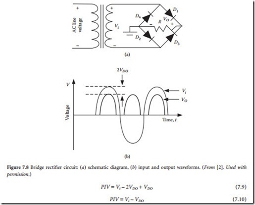
The full-wave rectifier requires a center-tapped transformer. The bridge rectifier is an alternative imple- mentation of the full-wave circuit [2]. (See Figure 7.8a.) This rectifier uses four diodes and does not require a center-tapped transformer. Figure 7.8b shows the input and output voltage waveforms for the bridge rectifier. During the positive half cycles of the input voltage, Vi is positive and the current is con- ducted through diode D1, resistor R, and diode D2. Meanwhile, diodes D3 and D4 will be reverse-biased. During the positive half-cycle, because two diodes are conducting, the output voltage will be Vi – 2VDO. During the negative half-cycle, the voltage Vi will be negative, and diodes D3 and D4 are forward-biased; the current through R follows the same direction as in the case of the positive half-cycle.
During positive halfcycle, the reverse voltage across D3 can be determined from the loop formed by D3, R, and D2 as VD3 (reverse) = VO + VD2 (forward) (7.8) The maximum value of VD3 occurs at the peak of VO and is given by
The PIV is about half the value for the full-wave rectifier with a center-tapped transformer, which is an advantage of the bridge rectifier.
Voltage Multiplier
The dc output voltage (Vdc) in a rectifier circuit is limited by the peak value of the ac voltage applied (VI) [2]. Figure 7.9a shows the voltage doubler circuit composed of a clamp formed by C1 and D1 and a peak rectifier formed by D2 and C2. When excited by a sinusoid of amplitude Vp, the output of the clamping section reaches the negative peak value of –2Vp, as shown in Figure 7.9b. By connecting additional diode- capacitor circuits, it is possible to generate rectifier circuits that triple and quadruple the input voltage.
Polyphase Rectifier Circuits
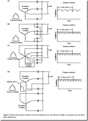
High-voltage power supplies typically used in vacuum tube circuits incorporate multiphase rectification of the ac line voltage. Common configurations include 3-, 6-, and 12-phase. Three-phase rectification is the most common. Figure 7.10 illustrates four approaches to three-phase rectification:
• Three-phase half-wave wye, Figure 7.10a. Three half-wave rectifiers are used in each leg of the secondary Y, forming one phase. In such an arrangement, each diode carries current one third of each cycle, and the output wave pulses at three times the frequency of the ac supply. In order to avoid direct-current saturation in the transformer, it is necessary to employ a three-phase trans- former rather than three single-phase transformers.
• Three-phase full-wave bridge, Figure 7.10b. Six diodes are used in this circuit to produce a low ripple output with a frequency of 6 times the input ac waveform. It is permissible in this configuration to use three single-phase transformers, if desired.
• Six-phase star, Figure 7.10c. This circuit, also known as a three-phase diametric configuration, uses six diodes with a transformer secondary configured as a star, as illustrated in the figure. The output ripple frequency is six times the input ac waveform.
• Three-phase double-wye, Figure 7.10d. This circuit uses six diodes and a complicated configuration of transformer windings. Note the balance coil (interphase transformer) in the circuit.
The relative merits of these rectifier configurations are listed in Table 7.2.
Polyphase rectifiers are used when the dc power required is on the order of 2 kW or more. The main advantages of a polyphase power supply over a single-phase supply include the following:
• Division of the load current between three or more lines to reduce line losses.
• Significantly reduced filtering requirements after rectification because of the low ripple output of a polyphase rectifier.
• Improved voltage regulation when using an inductive-input filter. Output voltage soaring is typ- ically 6% or less from full load to no load conditions.
• Greater choice of output voltages from a given transformer by selection of either a delta or wye configuration.
The main disadvantage of a polyphase system is its susceptibility to phase imbalance. Resulting operational problems include increased ripple at the output of the supply and uneven sharing of the load current by the transformer windings.
