Conducting materials
Strictly, conducting materials fall into three groups, which are conductors, semiconductors and imperfect insulators. Insulators have been discussed in section 3.3, so the focus here is on conductors and semiconductors.
Conductors
In general, metals and alloys are conductors of electricity. The conductivity in metals such as copper and aluminium is due to electrons that are attracted to the positive terminal when a voltage is applied. The freedom with which the electrons can move determines the conductivity and resistivity. The restraints on electron movements are impurities, stresses and thermal lattice vibrations; therefore, to obtain the highest conductivity the metal must be very pure and in the annealed state. With increasing temperature the thermal lattice vibrations increase and conductivity is therefore reduced.
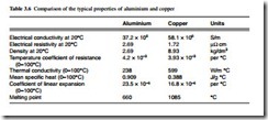
The principal material for commercial applications as conductors are the pure metals aluminium and copper, although very widely used are the alloys of these metals, with small additions of other elements to improve their properties for particular applications. Table 3.6 shows for comparison typical values of the key parameters for the two metals.
Copper and its alloys
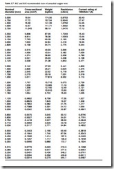
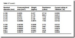
Copper has the highest electrical and thermal conductivity of the common industrial metals. It has good mechanical properties, is easy to solder, is readily available and has high scrap value. It is widely used in wire form, and Table 3.7 gives information for the commonly used wire sizes.
The electrical resistance of copper, as of all other pure metals, varies with temperature. The variation is sufficient to reduce the conductivity of pure copper at 100°C to about 76 per cent of its value at 20°C.
The resistance Rt1 at temperature t1 is given by the relationship
where αt is the constant-mass temperature coefficient of resistance of copper at the reference temperature t (°C). Although resistance may be regarded for practical
purposes as a linear function of temperature, the value of the temperature coefficient is not constant, but depends upon the reference temperature as given in eqn 3.2.
At 20°C, the value of α20 which is given by eqn 3.2 is 0.00393/°C, which is the value adopted by IEC. Multiplier constants and their reciprocals correlating the resistance of copper at a standard temperature with the resistance at other temperatures may be obtained from tables which are included in BS 125, BS 1432–1434 and BS 4109.
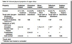
Cadmium copper, chromium copper, silver copper, tellurium copper and sulphur copper find wide application in the electrical industry where high conductivity is required. The key physical properties of these alloys are shown in Table 3.8. It can be seen that some of the alloys are deoxidized and some are ‘tough pitch’ (oxygen containing) or deoxidized. Tough pitch coppers and alloys become embrittled at elevated temperatures in a reducing atmosphere, and where such conditions are likely to be met, oxygen-free or deoxidized materials should be used.
Cadmium copper has greater strength than ordinary copper under both static and alternating stresses and it has better resistance to wear. It is particularly suitable for the contact wires in electric railways, tramways, trolley buses, gantry cranes and similar equipment, and it is also used in overhead telecommunication lines and transmission lines of long span. It retains its hardness and strength in temperatures at which high- conductivity materials would soften, and is used in electrode holders for spot and seam welding of steel, and it has also been used in commutator bars for certain types of motor. Because it has a comparatively high elastic limit in the work-hardened condition, it is also used in small springs required to carry current, and it is used as thin hard- rolled strip for reinforcing the lead sheaths of cables which operate under internal pressure. Castings of cadmium copper have some application in switchgear components and in the secondaries of transformers for welding machines. Cadmium copper can be soft soldered, silver soldered and brazed in the same way as ordinary copper, although special fluxes are required under certain conditions, and these should contain fluo- rides. Since it is a deoxidized material there is no risk of embrittlement by reducing gases during such processes.
Chromium copper is particularly suitable for high-strength applications such as spot and seam types of welding electrodes. Strip and, to a lesser extent, wire are used for light springs which carry current. In its heat-treated state, the material can be used at temperatures up to 350°C without risk of deterioration of properties, and it is used for commutator segments in rotating machines where the temperatures are higher than normal. In the solution heat-treated condition, chromium copper is soft and can be machined; in the hardened state it is not difficult to cut but it is not free-machining like leaded brass or tellurium copper. Joining methods similar to cadmium copper are applicable, and chromium copper can be welded using gas-shielded arcs.
Silver copper has the same electrical conductivity as ordinary high-conductivity copper, but its softening temperature, after hardening by cold work, is much higher and its resistance to creep at moderately elevated temperatures is enhanced. Since its out- standing properties are in the work-hardened state, it is rarely required in the annealed condition. Its principal uses are in electrical machines which operate at high temperatures or are exposed to high temperatures in manufacture. Examples of the latter are soft soldering or stoving of insulating materials. Silver copper is available in hard drawn or rolled rods and sections, especially those designed for commutator segments, rotor bars and similar applications. Silver copper can be soft soldered, silver soldered, brazed or welded without difficulty but the temperatures involved in all these processes are sufficient to anneal the material, if in the cold-worked condition. Because the tough pitch material contains oxygen as dispersed particles of cuprous oxide, it is also impor- tant to avoid heating it to brazing and welding temperatures in a reducing atmosphere. In the work-hardened state, silver copper is not free-cutting, but it is not difficult to machine.
Tellurium copper offers free-machining, high electrical conductivity, with retention of work hardening at moderately elevated temperatures and good corrosion resistance. It is unsuitable for most types of welding, but gas-shielded arc welding and resistance welding can be done with care. A typical application is magnetron bodies, which are
often machined from solid. Tellurium copper can be soft soldered, silver soldered and brazed without difficulty. For tough pitch, brazing should be done in an inert or slightly oxidizing atmosphere since reducing atmospheres are conducive to embrittlement. Deoxidized tellurium copper is not subject to embrittlement.
Sulphur copper is free-machining and does not have the tendency of tellurium copper to form coarse stringers in the structure which can affect accuracy and finish. It has greater resistance to softening than high-conductivity copper at moderately high temperatures and gives good corrosion resistance. Sulphur copper has applications in all machined parts requiring high electrical conductivity, such as contacts and connectors; its joining characteristics are similar to those of tellurium copper. It is deoxidized with a controlled amount of phosphorus and therefore does not suffer from hydrogen embrittlement in normal torch brazing, but long exposure to a reducing atmosphere can result in loss of sulphur and consequent embrittlement.
Aluminium and its alloys
For many years aluminium has been used as a conductor in most branches of electrical engineering. Several aluminium alloys are also good conductors, combining strength with acceptable conductivity. Aluminium is less dense and cheaper than copper, and its price is not subject to the same wide fluctuations as copper. World production of aluminium has steadily increased over recent years to overtake that of copper, which it has replaced in many electrical applications.
There are two specifications for aluminium, one for pure metal grade 1E and the other for a heat-treatable alloy 91E. Grade 1E is available in a number of forms which are extruded tube (E1E), solid conductor (C1E), wire (G1E) and rolled strip (D1E). The heat-treatable alloy, which has moderate strength and a conductivity approaching that of aluminium, is available in tubes and sections (E91E).
The main application areas are as follows.
Busbars. Although aluminium has been used as busbars for many years, only recently has it been accepted generally. The electricity supply industry has now adopted alu- minium busbars as standard in 400 kV substations, and they are also used widely in switchgear, plating shops, rising mains and in UK aluminium smelting plants. Sometimes busbars are tin-plated in applications where joints have to be opened and re-made frequently.
Cable. The use of aluminium in wires and cables is described at length in Chapter 9. Aluminium is used extensively in cables rated up to 11 kV and house wiring cable above 2.5 mm2 is also available with aluminium conductor.
Overhead lines. The Aluminium Conductor Steel Reinforced (ACSR) conductor referred to in section 13.3 and Fig. 13.3 is the standard adopted throughout the world, although in USA Aluminium Conductor Aluminium alloy wire Reinforced (ACAR) is rapidly gaining acceptance; it offers freedom from bimetallic corrosion and improved con- ductance for a given cross section.
Motors. Aluminium is cast into the cage rotors of induction motors forming the rotor bars and end rings. Motor frames are often die-cast or extruded from aluminium, and shaft-driven cooling fans are sometimes of cast aluminium.
Foil windings. These are suitable for transformers, reactors and solenoids. They offer better space factor than a wire-wound copper coil, the aluminium conductor occupy- ing about 90 per cent of the space, compared to 60 per cent occupied by copper. Heat transfer is aided by the improved space factor and the reduced insulation that is needed in foil windings, and efficient radial heat transfer ensures an even temperature gradient. Windings of transformers are described in greater depth in section 6.2.2.
Heating elements. These have been developed in aluminium but they are not widely used at present. Applications include foil film wallpaper, curing concrete and possibly soil warming.
Heat sinks. They are an ideal application for aluminium because of its high thermal conductivity and the ease of extrusion or casting into solid or hollow shapes with inte- gral fins. They are used in a variety of applications such as semiconductor devices and transformer tanks. The low weight of aluminium heat sinks make them ideal for pole- mounted transformers and there is the added advantage that the material does not react with transformer oil to form a sludge.
Resistance alloys
There are many alloys with high resistivity, the two main applications being resistors and heating elements.
Alloys for standard resistors are required to have a low temperature coefficient of resistivity in the region of room temperature. The traditionally used alloy is Manganin, but this has increasingly been replaced by Ni–Cr–Al alloys with the trade names Karma and Evanohm. The resistivity of these alloys is about 1.3 µΩ m and the temperature coefficient is ± 0.5 × 10⁻⁵/°C. For lower precision applications copper–nickel alloys are used, but these have a lower resistivity and a relatively high thermo emf against copper.
For heating elements in electric fires, storage heaters and industrial and laboratory furnaces there is a considerable range of alloys available. A considerable resistivity is required from the alloy in order to limit the bulk of wire required, and the temperature coefficient of resistivity must be small so that the current remains reasonably constant with a constant applied voltage. The Ni–Cr alloys are used for temperatures up to 1100°C, and Cr–Fe–Al alloys are used up to 1400°C. Ceramic rods are used for higher temperatures and silicon carbide may be used up to 1600°C. For even higher temperatures, the cermets MoSi2 and Zircothal are used. The maximum temperature at which the materials may be used depends on the type of atmosphere.
Semiconductors
A semiconductor is able to conduct electricity at room temperature more readily than an insulator but less readily than a conductor. At low temperatures, pure semiconduc- tors behave like insulators. When the temperature of a semiconductor is increased, or when it is illuminated, electrons are energized and these become conduction electrons. Deficiencies or ‘holes’ are left behind; these are said to be carriers of positive electricity. The resulting conduction is called intrinsic conduction.
The common semiconductors include elements such as silicon, germanium and selenium and compounds such as indium arsenide and gallium antimonide. Germanium was originally used for the manufacture of semiconductor devices, but because of
resistivity problems and difficulty of supply it was replaced by silicon which is now the dominant material for production of all active devices such as diodes, bipolar transistors, MOSFETs, thyristors and IGBTs. The principles of operation of the MOSFET and IGBT are described briefly in section 11.3.
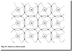
Both silicon and germanium are group IV elements of the periodic table, having four electrons in their outer orbit. This results in a diamond-type crystal giving a tight bond of the electrons. Figure 3.8 shows the atoms in a silicon crystal. Each atom is surrounded by eight electrons, four of which are its own and four are from neighbour- ing atoms; this is the maximum number in an orbit and it results in a strong equilibrium. It is for this reason that pure crystals of silicon and germanium are not good conductors at low temperature.
Impurity effects and doping
The conductivity of group IV semiconductors like silicon can be greatly increased by the addition of small amounts of elements from group V (such as phosphorus, arsenic or tin) of group III (such as boron, aluminium, gallium or indium).
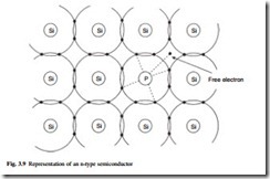
Phosphorus has five electrons in its outer shell and when an atom of phosphorus replaces an atom of silicon it generates a free electron, as shown in Fig. 3.9. This is called doping. The extra electrons are very mobile; when a voltage is applied they move very easily and a current passes. If 1016 phosphorus atoms/cm3 are added to a pure crystal, the electron concentration is greatly increased and the conductivity is increased by a factor of about a million. The impurities are called donor atoms and the material is an impurity semiconductor. This is called an n-type semiconductor, and n represents the excess of free electron carriers.
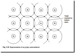
If the material is doped with group III atoms such as indium, then a similar effect occurs. This is shown in Fig. 3.10. The missing electron forms a ‘hole’ in the structure which acts as a positive carrier. This structure is known as a p-type semiconductor and p represents the excess of positive carriers. The impurities are called acceptor atoms.
A single crystal containing both n-type and p-type regions can be prepared by introducing the donor and acceptor impurities into molten silicon at different stages of the crystal formation. The resultant crystal has two distinct regions of p-type and n-type material, and the boundary joining the two areas is known as a p–n junction. Such a junction may also be produced by placing a piece of donor impurity material against the surface of a p-type crystal or a piece of acceptor impurity material against an n-type crystal, and applying heat to diffuse the impurity atoms through the outer layer.
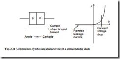
When an external voltage is applied, the n–p junction acts as a rectifier, permitting current to flow in only one direction. If the p-type region is made positive and the n-type region negative, a current flows through the material across the junction, but when the potential difference is reversed, no current flows. This characteristic is shown in Fig. 3.11.
The transistor
Many types of device can be built with quite elaborate combinations and constructions based around the n–p and p–n junction. Further information on these devices may be found in reference 3G.
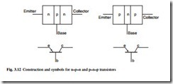
Possibly the most important single device is the transistor, in which a combination of two or more junctions may be used to achieve amplification. One type, known as the n–p–n junction transistor, consists of a very thin layer of p-type material between two sections of n-type material, arranged in a circuit shown in Fig. 3.12. The n-type material at the left of the diagram is the emitter element of the transistor, constituting the electron source. To permit the flow of current across the n–p junction, the emitter has a small negative voltage with respect to the p-type layer (or base component) that controls the electron flow. The n-type material in the output circuit serves as the collector element, which has a large positive voltage with respect to the base in order to prevent reverse current flow. Electrons moving from the emitter enter the base, are
attracted to the positively charged collector, and flow through the output circuit. The input impedance, between the collector and the base is low, whereas the output impedance between the collector and the base is high. Therefore, small changes in the voltage of the base cause large changes in the voltage drop across the collector resistance, making this type of transistor an effective amplifier.
Similar in operation to the n–p–n type is the p–n–p junction transistor also shown in Fig. 3.12. This also has two junctions and is equivalent to a triode vacuum tube.
Other types, such as the n–p–n–p junction transistor, provide greater amplification than these two-junction transistors.
Printed circuits and integrated circuits
A printed circuit is an electrical circuit made by printing and bonding conducting material as a network of fine threads on a thin ceramic or polymer insulating sheet. This replaces the wiring used in conventional circuits. Other elements such as transistors, resistors and capacitors can be deposited onto the same base as the printed circuit.
An integrated circuit is effectively a combination of many printed circuits. It is formed as a single unit by diffusing impurities into single-crystal silicon, which then serves as a semiconductor material, or by etching the silicon by means of electron beams. Several hundred integrated circuits (ICs) are made at a time on a thin wafer several centimetres in diameter, and the wafer is subsequently sliced into individual ICs called chips.
In large scale integration (LSI), several thousand circuit elements such as resistors and transistors are combined in a 5 mm square area of silicon no more than 0.5 mm thick. Over 200 such circuits can be arrayed on a silicon wafer 100 mm in diameter.
In very large scale integration (VLSI), hundreds of thousands of circuit elements fit onto a single silicon chip. Individual circuit elements on a chip are interconnected by thin metal or semiconductor films which are insulated from the rest of the circuit by thin dielectric layers. This is achieved by the formation of a silicon dioxide layer on the silicon wafer surface, silicon dioxide being an excellent dielectric. Metal Oxide Semiconductor Field Effect Transistors (MOSFETs) are made using this technique. These transistors are used for high-frequency switching applications and for random access memories in computers. They have very high speed and low power consumption.
The microprocessor
The microprocessor is a single chip of silicon which has the ability to control processes. It can form the central processing unit (CPU) of a small computer and it can be used in a wide range of other applications. A microprocessor may incorporate from a thou- sand up to several hundred thousand elements. It typically contains a read-only memory (ROM), that is a memory that can be read repeatedly but cannot be changed, but it may also have some random access memory (RAM) for holding transient data. Also present in a microprocessor are registers for holding computing instructions, for holding the ‘address’ of each instruction in turn and for holding data, and a logic unit. Interfaces for connecting with external memories and other systems are included as required.
The microprocessors used in personal computers have been the subject of intensive development during the 1990s. The speed of operation is usually defined as a frequency and chips with frequencies of 3 GHz or higher are now available; this corresponds to an individual operation time of 0.33 nanoseconds. Personal computers with hard disk capacities of 80 Gb and laptop computers of 60 Gb can now be obtained. The amount
of information that can be transferred in parallel and held in registers is known as a bit, and 64-bit processors are now available.
Superconductors
The ideal superconducting state is characterized by two fundamental properties, which are the disappearance of resistance when the temperature is reduced to a critical value, and the expulsion of any magnetic flux in the material when the critical temperature (Tc) is reached. Superconductivity was first discovered in the element mercury, in 1911. Other elements have subsequently been found to exhibit superconductivity and theories have been developed to explain the phenomenon. The critical temperatures for these materials were typically about 10 K (−263°C), which meant that they had to be cooled with liquid helium at 4 K. In general these materials have been of academic interest only because they could only support a low current density in a low magnetic field without losing their superconducting properties.
In the 1950s a new class of materials was discovered. These are the metallic alloys, the most important among them being niobium titanium and niobium tin. The highest critical temperature achieved by these materials is 23.2 K and they can be used to pro- duce magnetic flux densities of over 15 T. The main commercial application for these low-Tc superconductors is for magnets in medical imaging equipment which require the high fields to excite magnetic resonance in nuclei of hydrogen and other elements. The magnet or solenoid of the magnetic resonance imaging (MRI) unit has an internal diameter of about 1.2 m and the patient to be examined is put into this aperture. The image from the resonance test shows unexpected concentrations of fluids or tissue and enables a diagnosis. Superconducting magnets producing high magnetic fields are also used in magnetic research and in high-energy physics research; other applications such as dc motors and generators, levitated trains, cables and ac switches have been explored but the complexity and high cost of providing the liquid helium environment prevented commercial development in most cases.
In late 1986 a ceramic material LaBaCuO was discovered to be superconducting at 35 K and in 1987 the material YBaCuO was found to have a critical temperature of 92 K. Since that time the critical temperatures of these new high temperature super- conducting (HTS) materials has progressively increased to over 130 K. Examples of these are BiSrCaCuO (with a Tc of 106 K), ThBaCaCuO (Tc of 125 K) and HgBaCaCuO (Tc of 133 K). The enormous significance of these discoveries is that these materials will be superconducting in liquid nitrogen, which has a boiling point of 77 K and is much easier and cheaper to provide than helium.
Much work has been directed towards finding materials with higher Tc values but this has remained at 133 K for some time. However, considerable effort with resulting success has been directed to the production of suitable HTS conductors. The HTS mate- rial is very brittle and it is deposited using laser deposition onto a suitable substrate tape. The tape is 3 mm wide and cables of up to 600 m in length have been produced.
There are many trials being made of the application of the HTS cables throughout the world including USA, Europe and Japan. There are prototypes of power trans- formers, underground power cables, large motors and generators, and fault current limiters in active development and in use. The electricity supply of the City of Geneva in Switzerland is completely provided by power transformers wound with HTS conductors. Detroit is being re-equipped with HTS power cable for its transmission system and copper cables weighing over 7 tons are being replaced with HTS cables of less than 0.12 tons. These and other developments will help to establish the long-term
feasibility of the HTS material. It is expected that there will be definite power saving from the use of HTS.
Small-scale applications which use HTS material include SQUIDS (Superconducting QUantum Interference DeviceS) which measure very low magnetic fields. They are applied in measurements in biomagnetism (investigations of electrical activity in the heart, brain and muscles) and in geophysics for the study of rock magnetism and anomalies in the earth’s surface.
Standards
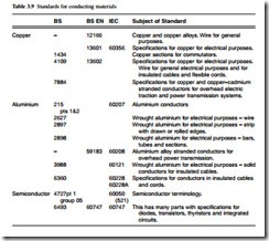
Each country has in the past had its own standards for materials. Over the past twenty years or so there has been a movement towards international standards which for elec- trical materials are produced by IEC. When an IEC standard is produced the member countries copy this standard and issue it under their own covers (Table 3.9).
Acknowledgement
My thanks are due to the staff of the University of Sunderland and of the City of Sunderland College for help with this chapter.
