Grounding Signal Cables
Proper ground-system installation is the key to minimizing noise currents on signal-carrying cables. Audio, video, and data lines are often subject to ac power noise currents and RFI. The longer the cable run, the more susceptible it is to disturbances. Unless care is taken in the layout and installation of such cables, unac- ceptable performance of the overall system can result.
Analyzing Noise Currents
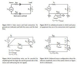
Figure 20.32 shows a basic source and load connection. No grounds are present, and both the source and the load float. This is the optimum condition for equipment interconnection. Either the source or the load can be tied to ground with no problems, provided only one ground connection exists. Unbalanced sys- tems are created when each piece of equipment has one of its connections tied to ground, as shown in Figure 20.33. This con- dition occurs if the source and load equipment have unbalanced (single-ended) inputs and outputs. This type of equipment uti- lizes chassis ground (or common) for one of the conductors. Problems are compounded when the equipment is separated by a significant distance.
As shown in Figure 20.34, a difference in ground potential causes current flow in the ground wire. This current develops a voltage across the wire resistance. The ground-noise voltage adds directly to the signal itself. Because the ground current is usually
the result of leakage in power transformers and line filters, the 60 Hz signal gives rise to hum of one form or another. Reducing the wire resistance through a heavier ground conductor helps the situation, but cannot eliminate the problem.
By amplifying both the high side and the ground side of the source and subtracting the two to obtain a difference signal, it is possible to cancel the ground-loop noise. This is the basis of the differential input circuit, illustrated in Figure 20.35. Unfortunately, problems still can exist with the unbalanced-source-to- balanced-load system. The reason centers on the impedance of the unbalanced source. One side of the line will have a slightly lower amplitude because of impedance differences in the output lines. By creating an output signal that is out of phase with the original, a balanced source can be created to eliminate this error. (See Figure 20.35.) As an added benefit, for a given maximum output voltage from the source, the signal voltage is doubled over the unbalanced case.
Types of Noise
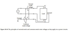
Two basic types of noise can appear on ac power, audio, video, and computer data lines within a facility: normal mode and common mode. Each type has a particular effect on sensitive load equipment. The nor- mal-mode voltage is the potential difference that exists between pairs of power (or signal) conductors. This voltage also is referred to as the transverse-mode voltage. The common-mode voltage is a potential difference (usually noise) that appears between the power or signal conductors and the local ground ref- erence. The differences between normal-mode and common-mode noise are illustrated in Figure 20.36.
The common-mode noise voltage will change, depending upon what is used as the ground reference point. It is often possible to select a ground reference that has a minimum common-mode voltage with respect to the circuit of interest, particularly if the reference point and the load equipment are connected by a short conductor. Common-mode noise can be caused by electrostatic or electromagnetic induction.
In practice, a single common-mode or normal-mode noise voltage is rarely found. More often than not, load equipment will see both common-mode and normal-mode noise signals. In fact, unless the facility wiring system is unusually well-balanced, the noise signal of one mode will convert some of its energy to the other mode.
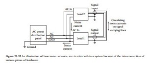
Common-mode and normal-mode noise disturbances typically are caused by momentary impulse voltage differences among parts of a distribution system that have differing ground potential references. If the sections of a system are interconnected by a signal path in which one or more of the conductors are grounded at each end, the ground offset voltage can create a current in the grounded signal conductor. If noise voltages of sufficient potential occur on signal-carrying lines, normal equipment operation can be disrupted. (See Figure 20.37.)
Noise Control
Noise control is an important aspect of computer and electronic system design and maintenance [2]. The process of noise control through proper grounding techniques is more correctly called referencing. For this discussion, electronic systems can be viewed as a multiplicity of signal sources transmitting signals to a multiplicity of loads. Practically speaking, the impedance of the signal return path is never
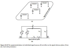
zero, and dedicated return paths for each source-load pair are not always practical. Packaged electronics systems typically incorporate a common signal reference plane that serves as a common return path for numerous source-load pairs. (See Figure 20.38a.) The signal reference plane may be a large dedicated area on a circuit board, the metal chassis or enclosure of the electronic equipment, or the metal frame or mounting rack that houses several different units. Ideally, the signal reference plane offers zero impedance to the signal current. Practically, however, the signal reference plane has a finite impedance. The practical result is illustrated in Figure 20.38b and is called common-impedance or conductive coupling.
Because a practical signal reference plane has a finite impedance, current flow in the plane will produce potential differences between various points on the plane. Source-load pairs referenced to the plane will, therefore, experience interference as a result. ZR is common to both circuits referenced to the plane in Figure 20.38b. Thus, I1 and I2 returning to their respective sources will produce interference voltages by flowing through ZR. The total interference voltage drop seen across ZR causes the source reference A to be at a different potential than the load reference B. This difference in potential is often called ground voltage shift (even though ground may not even be involved) and is a major source of noise and interference in electronic circuits.
Ground voltage shifts can also be caused by electromagnetic or electrostatic fields in close proximity to the source-load pairs. The interference source induces interference voltages into any closed loop by antenna action. This loop is called a ground loop (even though ground may not be involved). Interference voltages can be minimized by reducing the loop area as much as possible. This can be very difficult if the loop includes an entire room. The interference voltage can be eliminated entirely by breaking the loop.
Within individual electronic equipments, the signal reference plane consists of a metal plate or the metal enclosure or a rack assembly, as previously discussed. Between units of equipment that are located in different rooms, on different floors, or even in different buildings, the signal reference planes of each unit must be connected together via interconnected wiring such as coax shields or separate conductors. This action, of course, increases the impedance between signal reference planes and makes noise control more difficult. Reducing noise caused by common-impedance coupling is a matter of reducing the impedance of the interconnected signal reference planes.
Regardless of the configuration encountered (i.e., circuit board, individual electronic equipment, or equipment remotely located within a facility or in separate buildings), the next question to be answered is, Should the signal reference be connected to ground? Floating signal grounding, single-point grounding, and multipoint grounding are methods of accomplishing this signal-reference-to-ground connection.
IEEE Standard 1100 recommends multipoint grounding for most computers. For effective multi- point grounding, conductors between separate points desired to be at the same reference potential should be less than 0.1 wavelength (λ/10) of the interference or noise-producing signal. Longer conductor lengths will exhibit significant impedance because of the antenna effect and become ineffective as equalizing conductors between signal references. On printed circuit cards or within individual electronics equip- ments, short conductor lengths are usually easy to achieve. For remotely located equipments, however, short equalizing conductor lengths may be impossible. Equipment in relatively close proximity can be equalized by cutting bonding conductors to an odd multiple of λ/2 at the noise frequency. The distribution of standing waves on bonding conductors is illustrated in Figure 20.39. The impedance, Z, is minimum for odd multiples of λ/2 but maximum for odd multiples of λ/4.
For remotely located electronics equipment within the same room, equalizing potential between respective signal reference systems may have to be accomplished with an equipotential plane. An ideal equipotential signal reference plane is one that has zero volts (thus zero impedance) between any two points on the plane. Because an ideal equipotential plane is not attainable, a nominal equipotential plane is accepted. Multipoint grounding connections are made to the plane, which insures minimum ground voltage shift between signal reference systems connected to the plane. Collectively, the current flow in an equipotential plane can be quite large. Between any two equipments however, the current flow should be low because of the many current paths available.
Practical versions of an equipotential plane include the following:
• Bolted stringer system of a raised computer-room floor
• Flat copper strips bonded together at 2-ft centers
• Copper conductors bonded together at 2-ft centers
• Single or multiple, flat copper strips connected between equipment
