The flip-flop belongs to a category of digital circuits called multivibrators. A multivibrator is a regenerative circuit with two active devices. It is designed so that one device conducts while the other device is cut off. Multivibrators can store binary numbers, count pulses, synchronize arithmetic operations, and perform other essential functions in digital systems.
There are three types of multivibrators: bistable, monostable, and astable. The bistable multivibrator is called a flip-flop.
A flip-flop is a bistable multivibrator whose output is either a high or low voltage, a 1 or a 0. The output stays high or low until an input called a trigger is applied.
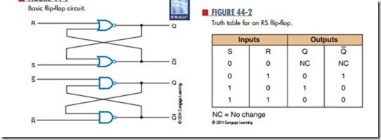
The basic flip-flop is the Rs flip-flop. It is formed by two cross-coupled NOR or NAND gates (Figure 44-1). The RS flip-flop has two outputs, Q and Q, and two controlling inputs, R (Reset) and S (Set). The outputs are always opposite or complementary: If Q 5 1, then Q 5 0, and vice-versa.
To understand the operation of the circuit, assume that the Q output, R input, and S input are all low. The low on the Q output is connected to one of the inputs of gate 2. The S input is low. The output of gate 2 is high. This high is coupled to the input of gate 1,
holding its output to a low. When the Q output is low, the flip-flop is said to be in the RESET state. It remains in this state indefinitely, until a high is applied to the S input of gate 2. When a high is applied to the S input of gate 2, the output of gate 2 becomes a low and is coupled to the input of gate 1. Because the R input of gate 1 is a low, the output changes to a high. The high is coupled back to the input of gate 2, ensuring that the Q output remains a low. When the Q output is high, the flip-flop is said to be in the SET state. It remains in the SET state until a high is applied to the R input, causing the flip-flop to RESET.
An “illegal” or “unallowed” condition occurs when a high is applied to both the R and S inputs simultane- ously. In this cas e, the Q and Q outputs both try to go low, but Q and Q cannot be in the same state at the same time without violating the definition of flip-flop operation. When the highs on the R and S inputs are removed simultaneously, both of the outputs attempt to go high. Because there is always some difference in the gates, one gate dominates and becomes high. This forces the other gate to remain low. An unpredictable mode of operation exists and therefore the output state of the flip-flop cannot be determined.
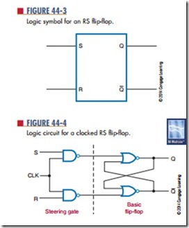
Figure 44-2 shows the truth table for operation of an RS flip-flop. Figure 44-3 is a simplified symbol used to represent an RS flip-flop.
Another type of flip-flop is called a clocked flip-flop. It is different from the RS flip-flop in that an additional input is required for operation. The third input is called the clock or trigger. Figure 44-4 shows a logic diagram for a clocked flip-flop. A high at either input of the flip-flop portion activates the flip- flop, causing it to change states. The portion labeled “steering gate” steers or directs the clock pulses to either input gate.
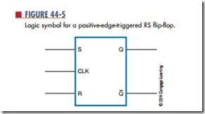
The clocked flip-flop is controlled by the logic state of the S and R inputs when a clock pulse is present. A change in the state of the flip-flop occurs only when the leading edge of the clock pulse is applied. The leading edge of the clock pulse is a positive-going transition (low to high). This means that the pulse goes from a zero voltage level to a positive voltage level. This is referred to as positive-edge-triggered (the edge of the pulse is what triggers the circuit).
As long as the clock input is low, the S and R in- puts can be changed without affecting the state of the flip-flop. The only time that the effects of the S and R inputs are felt is when a clock pulse occurs. This is referred to as synchronous operation. The flip-flop operates in step with the clock. Synchronous operation
is important in computers and calculators when each step must be performed in an exact order. Figure 44-5 shows the logic symbol used to represent a positive- edge-triggered RS flip-flop.
A D flip-flop is useful where only 1 data bit (1 or 0)is to be stored. Figure 44-6 shows the logic diagram for a D flip-flop. It has a single data input and a clock input. The D flip-flop is also referred to as a delay flip flop. The D input is delayed one clock pulse from get- ting to the output (Q). Sometimes the D flip-flop has Steering gate flip-flop a PS (preset) input and CLR (clear) input. The preset input sets output Q to a 1 when a low or 0 is applied to it. The clear input clears the Q output to a 0 when it is enabled by a low or 0. D flip-flops are wired together to form shift registers and storage registers. These registers are widely used in digital systems.
The JK flip-flop is the most widely used flip-flop. It has all the features of the other types of flip-flops. It is also edge triggered, accepting data only at the J and K inputs that are present at the active clock edge (high to low or low to high). This allows the accepting of input data on J and K at a precise instant. The logic diagram and symbol for the JK flip-flop is shown in Figure 44-7. J and K are the inputs. The significant feature of the JK flip-flop is that when both the J and K inputs are high, repeated clock pulses cause the output to toggle or change state. The two asynchronous inputs, PS (preset) and CLR (clear), override the
synchronous inputs, the J and K data inputs, and the clock input. JK flip-flops are widely used in many digital circuits, especially counter circuits. Counters are found in almost every digital system.
A latch is a device that serves as a temporary buffer memory. It is used to hold data after the input signal is removed. The D flip-flop is a good example of a latch device. Other types of flip-flops can also be used.
A latch is used when inputting to a seven-segment display. Without a latch, the information being dis- played is removed when the input signal is removed. With the latch, the information is displayed until it is updated.
Figure 44-8 shows a 4-bit latch. The unit has four D flip-flops enclosed in a single IC package. The E (enable) inputs are similar to the clock input of the D flip-flop. The data are latched when the enable line drops to a low, or 0. When the enable is high, or 1, the output follows the input. This means that the output will change to whatever state the input is in; for example, if the input is high, the output will become high; if the input is low, the output will become low. This condition is referred to as a transparent latch.
Questions
1. What is a flip-flop?
2. What are the different types of flip-flops?
3. What is meant by a clocked flip-flop?
4. What is the difference between an asynchronous input and a synchronous input?
5.What is a latch?


