FIELD-PROGRAMMABLE-LOGIC DEVICES
This section aims to provide a basic understanding of the designs, technologies and options available in the modern field-programmable-logic devices; field-programmable gate arrays (FPGAs), mask programmable gate arrays (MPGA), and programmable-logic devices (PLD), which include the simple PLD and complex PLD.
Field-programmable gate arrays (FPGA)
Field-programmable gate arrays (FPGA) are integrated circuits (ICs) that contain an array of logic cells surrounded by programmable I/O blocks. An FPGA can contain tens of thousands of programmable logic components called logic blocks or logic elements, and a hierarchy of recon- figurable interconnects that allow the blocks to be “wired together”, somewhat like a one-chip programmable breadboard. Logic blocks can be configured to perform complex combinational functions, or be merely simple logic gates such as AND, XOR and OR. In most FPGAs, the logic blocks also include memory elements, which may be simple flip-flops or more complete blocks of memory.
Xilinx co-founders, Ross Freeman and Benard Vonderschmitt, invented the first commercially viable, field-programmable gate array, the XC2064, in 1985. This had programmable gates and programmable interconnects between gates, and marked the beginnings of a new technology and market. Xilinx continued unchallenged and grew quickly from 1985 to the mid 1990s when competitors started to erode their market-share. By 1993, Actel, as one of competitors to Xilinx, was serving about 18 percent of the market.
In the early 1990s, FPGAs were primarily used in telecommunications and networking. By the end of the decade, FPGAs had found their way into automotive and industrial applications. A recent trend has been to take the coarse-grained architectural approach a step further, by combining the logic blocks and interconnects of traditional FPGAs with embedded microprocessors and related peripherals, to form a complete “system on a programmable chip”. An alternate approach to using hard-macro processors is to make use of the “soft” processor cores that are implemented within the FPGA logic.
Many modern FPGAs have the ability to be reprogrammed at runtime, which, as mentioned in the first paragraph of this subsection, leads to the idea of reconfigurable computing or reconfigurable systems. However dynamic reconfiguration at run-time is not supported, but instead the FPGA adapts itself to a specific program. Additionally, new, non-FPGA architectures are beginning to emerge. Software-configurable microprocessors adopt a hybrid approach by providing both an array of processor cores and also FPGA-like programmable cores on the same chip.
(1) Types and applications
From the application point of view, a field-programmable gate array (FPGA) is a semiconductor device that can be configured by the customer or designer after manufacturing, hence the name field- programmable. They are programmed by using a logic circuit diagram, or source code in a hardware description language (HDL). They can be used to implement any logical function that an ASIC could perform, but have the ability to update the in functionality after shipping, which offers advantages for many applications.
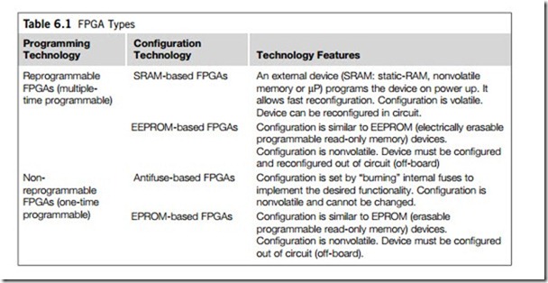
Two types of FPGAs have emerged. Firstly, reprogrammable (or multiple programmable) FPGAs including SRAM-based and EEPROM-based versions, and secondly non-reprogrammable (or one- time programmable) FPGAs, which are either antifuse-based or EPROM-based. Table 6.1 gives a technical overview.
Traditionally, FPGAs have been reserved for specific vertical applications where the volume of production is small. For these low-volume applications, the premium that companies pay in hardware costs per unit for a programmable chip is more affordable than the development resources spent on creating an ASIC. At present, FPGAs are used in applications ranging from data processing and storage, to instrumentation, telecommunications, and digital signal processing. Other terms for FPGA include logic cell array and programmable application-specific integrated chip.
FPGA architecture offers massive parallelism. This allows for considerable computational throughput even at a low clock rates. The inflexibility allows for even higher performance, by trading- off precision and range in the number format for an increased number of parallel arithmetic units. This has driven a new type of processing, called reconfigurable computing, where time-intensive tasks are offloaded from software to FPGAs. The adoption of FPGAs in high-performance computing is currently limited by the complexity of FPGA design that is possible, in comparison with conventional software. The extremely long turn-around times of current design tools, where a 4 8-hour wait is necessary after even minor changes to the source code is also a limiting factor.
Field-programmable gate arrays are available with different numbers of system gates, shift registers, logic cells, and lookup tables. Logic blocks or logic cells do not include I/O blocks, but generally contain a lookup table to generate any function of inputs, a clocked latch (flip-flop) to provide registered outputs, and control logic circuits for configuration purposes.
Logic cells are also known as logic array blocks, logic elements, or configurable logic blocks. Lookup tables or truth tables are used to implement a single logic function, by storing the correct output logic state in a memory location that corresponds to each particular combination of input variables.
FPGAs are available with many logic families, transistor-transistor logic and related technologies. By contrast, emitter coupled logic uses transistors to steer current through gates that compute logical functions. Another logic family, CMOS, uses a combination of p-type and n-type metal-oxide-semi- conductor field effect transistors to implement logic gates and other digital circuits. Logic families for FPGAs include crossbar switch technology, gallium arsenide, integrated injection logic, and silicon on sapphire. Gunning with transceiver logic and gunning with transceiver logic plus are also available.
FPGAs are available in a variety of IC package types and with different numbers of pins and flip- flops. Basic IC package types for field-programmable gate arrays include ball grid array, quad flat package, single in-line package, and dual in-line package. Many packaging variants are available.
As their size, capabilities, and speed increase, FPGAs are fulfilling functions, to the point where some are now marketed as full systems on chips (SoC).
(2) Architectures and designs
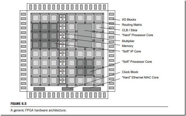
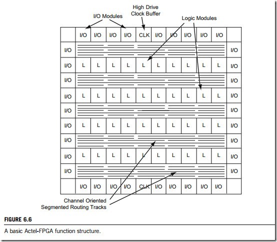
The hardware architecture, of FPGAs consists of an array of programmable logic blocks, routing matrix and global signals, input/output pads, multiplier, clock resources, memory cells and other advanced features. Figure 6.5 illustrates a generic example. Figure 6.6 gives an Actel FPGA function
as a basic example, showing several elemental components; logic modules/blocks, routing channels, I/ O modules, channeled interconnects, and clock resources.
(1) Logic modules/blocks
In a FPGA chip, the logic module should provide the user with the correct mixture of performance, efficiency, and ease of design required to implement the application. The logic module must be therefore be optimized to ensure that the many conflicting goals of the designer are achievable.
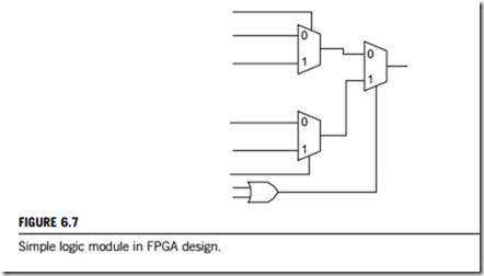
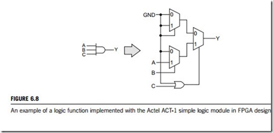
1. Simple logic module. The first Actel logic module was the Simple logic module, used in the ACT-1 family. Shown in Figure 6.7, it is a multiplexer-based logic module. Logic functions are implemented by interconnecting signals from the routing tracks to the data inputs and select lines of the multiplexers. Inputs can also be tied to a logical 1 or 0 if required, since these signals are always available in the routing channel. A surprising number of useful logic functions can be implemented with this module, providing the designer with an excellent mixture of logic capabilities. Figure 6.8
shows an example logic function implemented with the Actel simple logic module. Notice that latches can be implemented in a single logic module per bit and that registers require two logic modules per bit.
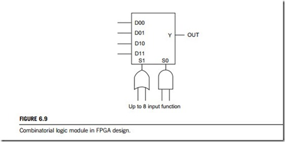
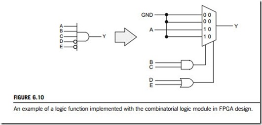
2. Combinatorial logic module. Some improvements were made to the simple logic module by replacing the simple logic module with two different logic modules, one for implementing combinatorial logic, (the combinatorial logic module) and one for implementing storage elements (the sequential logic module). The combinatorial logic module, shown in the diagram in Figure 6.9, is similar to the simple logic module, but an additional logic gate is placed on the first-level multiplexer. The added gate improves the implementation of some combinatorial functions. (Some five-input gates are now available.) Also, the first-level multiplexer lines in the simple logic module were combined in the combinatorial logic module. In the simple logic module, the separate multiplexer select lines were used to implement latches and registers efficiently. This was not required in the combinatorial logic module because of the addition of the sequential logic module. Figure 6.10 shows an example of a logic function implemented with the combinatorial logic module.
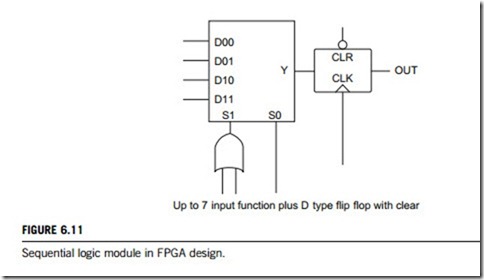
3. Sequential logic module. The sequential logic module, shown in Figure 6.11, has a combinatorial logic front-end with a dedicated storage element on the output. The storage element can be either a register or a latch. (It can also be bypassed so the logic module can be used as a combinatorial logic module.) The clock input can be either active high or active low. One of the logic gates is missing on the combinatorial logic diagram, making it slightly different from the combinatorial logic module. The exclusion of this one logic gate allows the reset signal, which is shared with the combinatorial logic section, to be made available to the storage element without increasing the number of total module inputs required. If the storage element is bypassed, the reset signal is used to implement the required combinatorial module input. In the Integrator Series, sequential and combinatorial modules are interleaved, resulting in a 50 50 mix of logic modules. This has been found to be an optimal mix for a wide variety of designs, and results in excellent utilization.
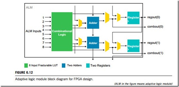
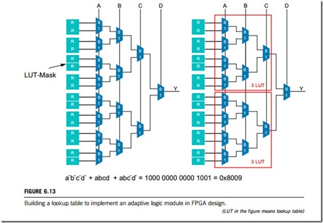
The key to a high-performance, area-efficient architecture is offered by an advanced logic module, adaptive logic module, which consists of combinational logic, two registers, and two adders as shown in Figure 6.12. The combinational portion has eight inputs and includes a lookup table, which can be divided between two tables using patented lookup technologies. An entire adaptive logic module is needed to implement an arbitrary six-input function, but because it has eight inputs to the combina- tional logic block, one adaptive logic module can implement various combinations of two functions. Lookup tables are built to help the description of the adaptive logic module. This is typically built out of SRAM bits to hold the configuration memory (CRAM) lookup table-mask and a set of multiplexers
to select the bit of CRAM that is to drive the output. To implement a k-input look-up table (k-lookup table is a lookup table that can implement any combination of k inputs) 2k SRAM bits and a 2k:1 multiplexer are needed. Figure 6.13 shows a 4-lookup table, which consists of 16 bits of SRAM and a 16:1 multiplexer implemented as a tree of 2:1 multiplexers. The 4-lookup table can implement any function of 4 inputs (A, B, C, D) by setting the appropriate value in the Look-up table-mask. To simplify the 4-Lookup table in Figure 6.13, it can also be built from two 3-lookup tables connected by a 2:1 multiplexer.
(2) Routing tracks
In addition to logic block architecture, another key FPGA feature is its routing architecture, which provides connectivity between different clusters of logic blocks, called logic array blocks. It is measured by the number of “hops” required to get from one logic array block to another. The fewer the number of hops, and more predictable the pattern, the better the performance and the easier it is for CAD (computer-aided design) tool optimization. Routing is organized as wires in a number of rows and columns.
There are two primary routing architectures in FPGAs; segmentation and buffer. Due to space considerations, this textbook does not discuss their details.
The routing process is generally separated into two phases using the divide and conquer paradigm. They are a global routing that balances the densities of all routing channels, and a detailed routing that assigns specific wiring segments for each connection. These two phases avoid congestion, and optimize the performance of the circuit, making sure all nets are routed such that wire length and capacitance on the path are minimized. By running both algorithms, a complete routing solution can be created. There are a number of routing algorithms that solve the problem using mixed routing i.e. both global and detailed routing at the same time, based on the idea that a higher integration of the two phases can prevent inaccurate estimation. The drawback of this approach is that as circuit size grows, this mixed routing becomes more complex and less scalable.
(3) Channelled interconnects
With some FPGAs, the routing tracks are also defined as channelled interconnects. For example, all Actel FPGAs use a channeled interconnect architecture to make connections between internal logic modules and device I/O pins (Figure 6.6). This architecture is similar to that of a channeled gate array, in that horizontal tracks span the length of the array with a variety of predefined segmentation lengths. This makes a huge amount of routing resources available and ensures that signals usually have the length of available track that they require. In addition, tracks can be joined to construct longer tracks, when required, by programming an interconnect fuse. Logic module outputs span four channels (two above and two below as shown in Figure 6.6) and can be connected to any track. This means that most signals require only two fuses to connect any logic module output to any logic module input. There are enough routing resources available in Actel FPGA devices so that place and route is an automatic task. No hand routing is required. For more details on the interconnect resources available in Actel FPGA devices, refer to the device family data sheets.
(4) I/O modules
Each FPGA family, either from different manufacturers or from the different versions from the same a manufacturer, has a slightly different I/O module. However, all the I/O modules in FPGAs were developed from the simple I/O module, optimized as an advanced I/O module for a new balance of speed and cost (value). More details on each I/O module can be found in the associated device data sheets and application notes.
1. Simple I/O module. The simple I/O module is a simple I/O buffer with interconnections to the logic array. All input, output, and three-state control signals are available to the array. Outputs are TTL (transistor-transistor logic) and CMOS compatible and sink or source about 10 mA at TTL levels.
2. Latched I/O module. The latched I/O module is used in the Integrator Series and is slightly more complicated than the simple module. It contains input and output latches that can be used as such, or when combined with internal latches, become input or output registers. Outputs are TTL and CMOS compatible and sink or source about 10 mA at TTL levels.
3. Registered I/O module. The registered I/O module is optimized for speed and functionality in synchronous system designs. It contains complete registers at both the input and output paths. Data can be stored in the output register, or they can bypass the register if the control bit is tied low. Both the output and input register can be cleared or preset via the global I/O signal, and both are clocked via another global I/O signal. Notice that the output of the output register can be selected as an input to the array. This allows state machines, for example, to be built right into the I/O module for fast clock-to- output requirements.
(5) Clock resources
Actel FPGA devices have a wide range of clocking flexibility. Every sequential element’s clock input can be connected to regular interconnects within the channel, as well as to optimized clocking resources. Regular interconnects offer the most flexibility, allowing for thousands of potential separate clocks. Each Actel device also has dedicated clocking resources on-chip to improve clock performance and to simplify the design of sequential signals. Clocking resources can also be used, in most cases, as high-drive global signals such as reset, output enable, or select signals. Each FPGA family is slightly different in the way it implements clocking functions. For more details on each type of clocking resource, refer to the associated device data sheets and application notes.
1. Routed clocks. All Actel FPGA families have one or two special buffers that provide high-drive, low-skew signals and that can be used to drive any signal requiring these characteristics. These routed clocks are distributed to every routing channel and are available to every logic module. This allows a routed clock signal to be used by both sequential and combinatorial logic modules, offering maximum flexibility with slightly lower performance than dedicated clocks.
2. Dedicated array clock. The Actel’s ACT-3 family has an additional clocking resource, consisting of a high-speed dedicated clock buffer that is optimized for driving sequential modules in the core array. This clock buffer can be driven from an external pin or from an internal signal. The dedicated array clock is optimized for driving sequential modules and cannot drive storage elements built from combinatorial modules.
3. Dedicated I/O clock. Another clocking resource consists of a high-speed dedicated clock buffer
optimized for driving the sequential modules in the I/O modules. It is optimized for driving I/O modules and cannot drive storage elements in the array. If all storage elements need to be driven from a common clock, the array clock and I/O clock can be connected together externally.
4. Quad clocks. Some of the FPGA family has an additional clocking resource consisting of four
special high-drive buffers called quadrant clocks. Each buffer provides a high-drive signal that spans about one-quarter of the device (a quadrant). These buffers can be used for fast local clocks (perhaps for pre-scaled shifters or counters), for wide-width selects, or for I/O enables. Note that since these are quadrant oriented, only a single quadrant clock can be used per quadrant. Quad clocks can be con- nected together internally to span up to one-half of the device. Additionally, the quad clocks can be sourced from internal signals as well as external pins. Thus they can be used as internally driven high fan-out nets.
(3) Programming and principles
Every FPGA relies on the underlying programming technology that is used to control the programmable switches to provide its programmability. There are a number available, and their differences have a significant effect on programmable-logic architecture. The approaches that have been used historically include EPROM, EEPROM, flash, SRAM (static-RAM), and antifuse programming technologies. Of these approaches, only the static memory, flash memory and antifuse approaches are widely used in modern FPGAs. The following will briefly review all modern FPGA programming technologies in order to provide a more comprehensive understanding of the FPGA working principle.
(a) Static memory programming technology
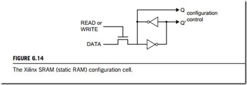
Static memory cells are the basis for SRAM programming technology, which is widely used, and can be found in the technical documents of FPGA superpowers such as Xilinx and Actel. In these devices, static memory cells are distributed throughout the FPGA to provide configurability. Most are used to set the select lines to multiplexers that steer interconnecting signals. An example of SRAM programming technology is shown in Figure 6.14, constructed from two cross-coupled inverters and using a standard CMOS process. The configuration cell drives the gates of other transistors on the chip by either turning pass transistors or transmission gates on to make a connection or off to break a connection.
The advantages of SRAM programming technology are the easy reuse of chips during proto- typing. The technology is also useful for upgrades, where a customer can be sent a new configuration file to reprogram a chip, rather than a new chip. On the other hand, its disadvantage is the need to maintain the power supplied to the programmable ASIC (at a low level) for the volatile SRAM to retain its connection information. The total size of an SRAM configuration cell plus the transistor switch that the SRAM cell drives is also larger than the programming devices used in the antifuse technologies.
(b) Floating-gate programming technology
One alternative programming technology, floating-gate programming, can addresses some of the shortcomings of static memory programming, and hence is used for flash and EEPROM memories’ programming. This floating-gate programming technology is achieved through a digital interface composed of a digital switch matrix and an analog/digital converter. Digital switches control the tunneling and injection voltages, and the digital decoders in order to provide individual access to the floating-gate transistors. An on-chip, specialized, analog/digital converter provides feedback to the programmer by outputting a digital signal with a pulse width that is proportional to the drain current of the floating-gate transistor currently being programmed. To avoid additional hardware on the proto- typing station, the FPGA that is used to implement the digital part of the system in operational mode is also used to implement the programming algorithms in configuration mode.
(c) Antifuse programming technology
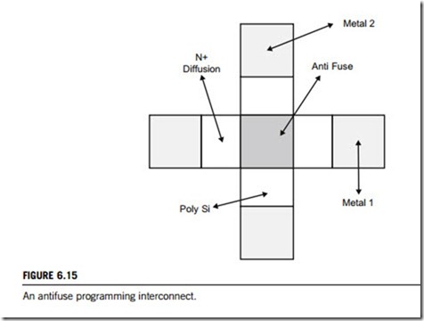
Antifuse programming is based on structures that exhibit very high resistance under normal circumstances, but can be programmably connected to create a low resistance link that is permanent. Different from SRAM and floating-gate programming technologies, the programmable
element, an antifuse, is used directly for transmitting FPGA signals. Two approaches have been used to implement antifuse; dielectric and metal. Direct antifuses, identified at the center of Figure 6.15, are composed of an oxide-nitride-oxide dielectric positioned between Nþ diffusion and polysilicon. The application of a high voltage causes the dielectric to break down, and form a conductive link with a resistance of typically between 100 and 600 ohms. The dielectric approach has been largely replaced by metal-to-metal-based antifuse. These antifuses are formed by silicon oxide between two metal layers. Again, a high voltage breaks down the antifuse and causes the fuse to conduct. The advantage of this method is that the on resistance can be between 20 and 100 ohms, and the fuse itself requires no silicon area. This metal-to-metal approach is used in recent FPGAs from Actel.
Antifuse technology is nonvolatile, so it is live at power-up and inherently very secure. Antifuse devices are mainly programmed using single-site or multi-site programmers. Types of programming for antifuse devices depend on the number and the type of devices to be programmed and are generally either device programmers or volume programming.
Device programmers are used to program a device before it is mounted on the system board, either before being soldered (usually done in production), or before putting it into a socket (used for pro- totyping). No programming hardware is required on the system board in this method, so no additional components or board space are required.
With the volume programming services, Actel can offer large volumes of parts which have been programmed, but programs that will not allow files to be sent off-site will not be able to use this approach. This includes Actel in-house programming, distributor programming centers, and inde- pendent programming centers.
Actel supplies two types of the programming software to serve for all the Actel programmers: single-site programmers and multiple-site programmers. Each version of the software enables users to select device, programming files, program, and verify the device.
Mask-programmable gate arrays (MPGA)
The mask-programmable gate array (MPGA) was developed to handle larger logic circuits. Although clearly not field-programmable devices, they did give considerable impetus to their indesign.
A common MPGA consists of several rows of transistors that can be interconnected in order to implement the desired logic circuits. User-specified connects are available, both within and between the rows. Customization is performed during chip fabrication by specifying the metal interconnect, which leads to setup costs long and high manufacturing times.
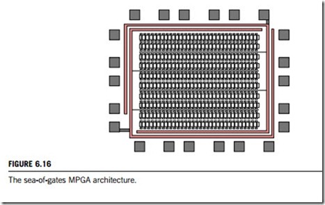
The most prevalent style of MPGA in current use is the sea-of-gates or sea-of-transistors archi- tecture. The core of a sea-of-gates MPGA is a continuous array of transistors in fixed positions, surrounded by I/O circuits and bonding pads. Wafers containing the core design are pre-fabricated up to the final metallization steps. These master or base wafers are held in stock by the vendor until a customer design is received. Then, one or more custom masks are created to define the user’s circuit with design specific metallization and contacts. Figure 6.16 shows the architecture of sea-of-gates MPGA.
Programmable-logic devices (PLD)
As already mentioned, logic devices can be classified into two broad categories; fixed and programmable. As the name suggests, the circuits in a fixed logic device are permanent, they perform one function or a set of functions, and once manufactured they cannot be changed. On the other hand, programmable-logic devices (PLDs) are standard, off-the-shelf parts that offer customers a wide range
of logic capacity, features, speed, and voltage characteristics; and hence these devices can be changed at any time (including at run-time) to perform any number of functions.
With fixed logic devices, the time required to go from design, to prototypes, to a final manufacturing run can between several months and more than a year, depending on the complexity of the device. If the device does not work properly, or if the requirements change, a new design then must be developed. With programmable-logic devices (PLDs), designers use inexpensive software tools to quickly develop, simulate, and test their designs. Then, a design can be quickly programmed into a device, and immediately tested in a live circuit. A key benefit of using PLDs is that customers can change the circuitry as often as they want during the design phase until it operates to their satisfaction.
Programmable-logic devices (PLDs) are designed with configurable logic and flip-flops linked together with programmable interconnects. They provide specific functions, including device-to- device interfacing, data communication, signal processing, data display, timing and control operations, and almost every other function a system must perform. Generally, PLDs are either simple programmable-logic devices (SPLDs), complex programmable-logic devices (CPLDs), or field- programmable-logic devices (FPGAs).
Programmable-logic devices are field-programmable gate arrays (FPGAs) or complex programmable-logic devices (CPLDs). The distinction between the two is often a little fuzzy, as manufacturers designing new, improved architectures. Together, CPLDs and FPGAs are often referred to as high- capacity programmable-logic devices.
Programming technologies for PLD devices are based on the different types of semiconductor memory. As new types of memories have been developed, the technology has been applied to the creation of new types of PLD devices major distinguishing feature between SPLDs, CPLDs, and FPGAs is the level of available logic. Today, SPLDs are devices that typically contain the equivalent of 600 or fewer gates, while CPLDs and FPGAs have thousands and more than several millions of gates available, respectively. FPGAs offer the highest amount of logic density, the most useful features, and the highest performance. They are used in a wide variety of applications, ranging from data processing and storage, to instrumentation, telecommunications, and digital signal processing. CPLDs, by contrast, offer much smaller amounts of logic up to about 10,000 gates, but they offer very predictable timing characteristics, and are therefore ideal for critical control applications. Some CPLDs require extremely low amounts of power and are very inexpensive, making them ideal for cost-sensitive, battery-operated, portable applications such as mobile phones and digital handheld assistants.
Because the commercially available SPLDs and CPLDs were and certainly will be change both their architectures and techniques very rapidly full, this subsection will not provide a list of all available types. Instead, this subsection will emphasize two key technologies used for programming and manufacturing; user-programming switch technologies and the ASIC packaging technologies, even though some features are common to FPGAs.
(1) User-programming switch technologies
For higher-density devices, where CMOS dominates the ASIC industry, different approaches to implementing programmable switches have been developed. For CPLDs the main switch technologies (in commercial products) are floating-gate transistors like those used in EPROM and EEPROM, and for FPGAs they are SRAM and antifuse. Each of these is briefly discussed below.
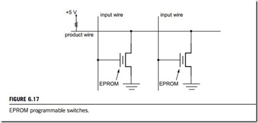
An EEPROM or EPROM transistor is used as a programmable switch for CPLDs (and also for many SPLDs) by placing the transistor between two wires to implement wired AND functions. This is illustrated in Figure 6.17, which shows EPROM transistors as they might be connected in an AND- plane of a CPLD. An input to the AND-plane can drive a product wire to logic level “0” through an EPROM transistor, if that input is part of the corresponding product term. For inputs that are not involved in a product term, the appropriate EPROM transistors are programmed to be permanently turned off. A diagram for an EEPROM based device would look similar.
Although there is no technical reason why EPROM or EEPROM could not be applied to FPGAs, current products are based on either SRAM or antifuse technologies, as discussed above.
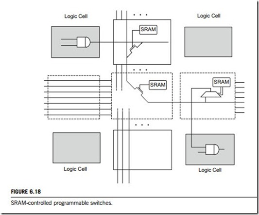
An example of SRAM-controlled switches is illustrated in Figure 6.18, showing SRAM cells controlling the gate nodes of pass-transistor switches, and the select lines of multiplexers that drive logic block inputs. The figure gives an example of the connection of one logic block (represented by the AND-gate in the upper left corner) to another through two pass-transistor switches, and then to a multiplexer, all controlled by SRAM cells. Whether an FPGA uses pass-transistors, or multiplexers, or both depends on the particular product.
(2) ASIC packaging technologies
The ASIC package must provide electrical connections to the chip for both signal and power transfer. The package must also physically support the relatively small and fragile ASIC die, and must protect it from moisture, dust, gases, and other potential contaminants. Finally, the package must provide heat transfer from the die to the ambient environment or to the second-level package in order to prevent performance and reliability degradation.
In fact, ASIC packaging can affect system performance as much or more than the selection of ASIC
design style or process technology. These influences upon system performance can be summarized as follows:
1. Degraded electrical performance (speed and power).
2. Increased size and weight.
3. Reduced testability.
4. Reduced reliability.
5. Increased cost.
Because of these influences, ASIC packaging has received considerable research and development attention particularly hybrid and multiple-chip module packaging techniques. This sections will only highlight a few of the relevant issues. The interested reader is referred to the professional handbooks devoted to this subject.
The traditional low-cost package of choice has been the dual-inline package. This package has a row of pins on each side, which are mounted into holes drilled through a printed-circuit board. Commercial dual-inline packages grow quite large as pin-count goes up, and are generally limited to a maximum of 64 pins. The pin-grid-array package was developed to increase pin density by placing leads under the entire bottom surface of the package. This technology provides well in excess of 300 pins per package, and like dual-inline packages requires through-hole printed-circuit board mounting with 100 mm lead spacing.
Surface-mount ASIC packages have now overtaken the traditional through-hole package market, even for cost-sensitive products. Here, a chip carrier, which may have leads on all four sides, is soldered directly onto pads on the surface of the printed-circuit board. Lead pitch on a surface mount component is typically 20 to 50 mils, compared to the 100 mil pitch of dual-inline packages and pin-grid arrays. Higher system packaging density is possible since the ASIC packages are smaller, through-holes are not needed, and components can be placed on both sides of the board without interference. This higher component density reduces parasitic capacitance and inductance and results in higher system operating speed. However, testing of these boards is much more difficult than through-hole printed-circuit boards. For example, traditional bed-of-nails-style board-level testers cannot be used to drive and observe signals from the back side of the board since all ASIC pins are not available on through-holes. In fact, the increasing use of surface-mount printed-circuit boards was a driving factor in the devel- opment and overwhelming acceptance of the IEEE Boundary Scan test standard (IEEE 1149.1).
The most promising new ASIC packaging technology is the ball-grid array. A ball-grid-array package provides high I/O density through its array of solder bumps on the underside of the package without requiring ultra-fine-pitch connections to the printed-circuit board. for example, a 1-inch- square quad-flat-packs package with a 50 mil lead pitch can provide 80 I/O connections. For the same package dimensions, a ball-grid-array package can provide 400 I/O connections. They have proved considerable interest since their introduction a few years ago. Motorola is developing a ball-grid-array package for its microcontrollers, Hitachi has planned to offer a micro-ball-grid-array package for its 0.5m mask-pin-grid arrays with up to 672 I/O connections, and Sandia National Labs is developing a mini-ball-grid-array package only slightly larger than the chip die which can accommodate more than 200 I/O connections.
A fundamental constraint imposed by ASIC packaging is the limited number of available pins. During the time when the on-chip ASIC gate count has increased by nearly six orders of magnitude, the number of available package pins has only increased by about two orders of magnitude. The most popular ASIC packages today are the pin-grid arrays, quad-flat-packs and thin-quad-flat-packs. The current trend in packaging is toward very tight lead pitches, staggered lead pitches, advanced array packages such as ball-grid array and flip-chip, and non-standard surface mount packages such as tape- automated bonding.
