Input Switching
The comments made about input connections are equally true for the necessary switching of the input signal sources. Separate, but mechanically interlinked, switches of the push- on, push-off type are to be preferred to the ubiquitous rotary wafer switch, in that it is much easier, with separate switching elements, to obtain the required degree of isolation between inputs and channels than would be the case when the wiring is crowded around the switch wafer.
However, even with separate push switches, the problem remains that the input connections will invariably be made to the rear of the amplifier/preamplifier unit, whereas the switching function will be operated from the front panel so that the internal connecting leads must traverse the whole width of the unit.
Other switching systems, based on relays, or bipolar or field effect transistors, have been introduced to lessen the unwanted signal intrusions, which may arise on a lengthy connecting lead. The operation of a relay, which will behave simply as a remote switch when its coil is energized by a suitable DC supply, is straightforward, although for
optimum performance it should either be hermetically sealed or have noble metal contacts to resist corrosion.
7.8.1 Transistor Switching
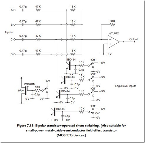
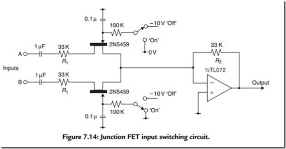
Typical bipolar and FET input switching arrangements are shown in Figures 7.13 and 7.14. In the case of the bipolar transistor switch circuit of Figure 7.13, the nonlinearity of the junction device when conducting precludes its use in the signal line; the circuit is therefore arranged so that the transistor is nonconducting when the signal is passing
through the controlled signal channel, but acts as a short-circuit to shunt the signal path to the 0-V line when it is caused to conduct.
In the case of the FET switch, if R1 and R2 are high enough, the nonlinearity of the conducting resistance of the FET channel will be swamped, and the harmonic and other distortions introduced by this device will be negligible (typically less than 0.02% at 1 V rms and 1 kHz).
The CMOS bilateral switches of the CD4066 type are somewhat nonlinear and have a relatively high level of breakthrough. For these reasons they are generally thought to be
unsuitable for high-quality audio equipment where such remote switching is employed to minimize cross talk and hum pick up.
However, such switching devices could well offer advantages in lower quality equipment where the cost savings is being able to locate the switching element on the printed circuit board, at the point where it was required, might offset the device cost.
Diode Switching
Diode switching of the form shown in Figure 7.15, while employed very commonly in RF circuitry, is unsuitable for audio use because of the large shifts in the DC level between the “on” and “off” conditions, which would produce intolerable “bangs” on operation.
For all switching, quietness of operation is an essential requirement, and this demands that care shall be taken to ensure that all of the switched inputs are at the same DC potential, preferably that of the 0-V line. For this reason, it is customary to introduce DC blocking capacitors on all input lines, as shown in Figure 7.16, and the time constants
of the input RC networks should be chosen so that there is no unwanted loss of low- frequency signals due to this cause.

