Integrated Circuit (Three Terminals) Voltage Regulator ICs
For output voltages up to ±24 V and currents up to 5 A, depending on voltage rating, a range of highly developed IC voltage regulator packages are now offered, having overcurrent (s/c) and thermal overload protection, coupled with a very high degree of output voltage stability, and coupled with a typical >60-dB input/output line ripple rejection. They are available most readily in +5 V and +15V/-15V output voltages because of the requirements of 5-V logic ICs and of IC op-amps, widely used in preamplifier circuits, for which ±15-V supply rails are almost invariably specified. Indeed, the superlative performance of contemporary IC op-amps designed for use in audio applications is such an attractive feature that most audio power amplifiers are now designed so that the maximum signal voltage required from the pre amp is within the typical 9.5-V rms output voltage available from such IC op-amps.
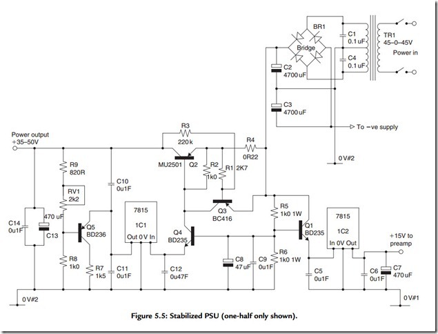
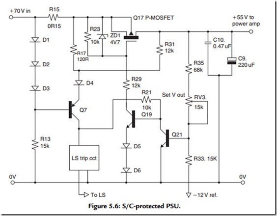
Higher voltage regulator ICs, such as the LM337T and the LM317T, with output voltages up to -37 and +37 V, respectively, and output currents up to 1.5 A are available but where audio amplifier designs require higher voltage-stabilized supply rails, the most common approaches are either to extend the voltage and current capabilities of the standard IC regulator by adding on suitable discrete component circuitry, as shown in Figure 5.5, or by assembling a complete discrete component regulator of the kind shown in Figure 5.6.
In the circuit arrangement shown for a single channel in Figure 5.5, a small-power transistor, Q1, is used to reduce the 55- to 60-V output from the unregulated PSU to a level that is within the permitted input voltage range for the 7815 voltage regulator IC (IC2). This is one of a pair providing a ±15-V DC supply for a preamplifier. A similar 15-V regulator IC (IC1) has its input voltage reduced to the same level by the emitter– follower Q4 and is used to drive a resistive load (R7) via the control transistor, Q5. If the output voltage, and consequently the voltage at Q5 base, is too low, Q5 will conduct, current will be drawn from the regulator IC (IC1), and, via Q4, from the base of the pass transistor, Q2. This will increase the current through Q2 into the output load and will increase the output voltage. If, however, the output voltage tends to rise to a higher level than that set by RV1, Q5 will tend toward cutoff and the current drawn from Q2 base will be reduced to restore the target output voltage level.
Overcurrent protection is provided by the transistor Q3, which monitors the voltage developed across R4 and restricts the drive to Q2 if the output current is too high.
Safe operating area conformity is ensured by the resistor R3, which monitors the voltage across the pass transistor and cuts off Q2 base current if this voltage becomes too high.
In the circuit of Figure 5.6, which is used as the power supply for an 80- to 100-W power MOSFET audio amplifier—again only one channel is shown—a P-channel power
MOSFET is used as the pass transistor and a circuit design based on discrete components is used to control the output voltage. In this, transistor Q21 is used to monitor the potential developed across R33 through the R35/RV3 resistor chain. If this is below the target value, current is drawn through Q19 and R29 to increase the current flow through the pass transistor (Q17). If either the output current or the voltage across Q17 is too high, Q7 is cut off and there is no current flow through Q18 into Q17 gate.
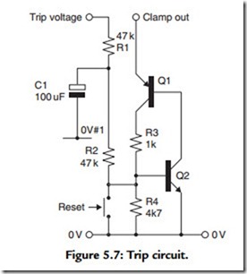
This regulator circuit allows electronic shut down of the power supply if an abnormal output voltage is detected across the LS terminals (due, perhaps, to a component failure). This monitoring circuit (one for each channel) is shown in Figure 5.7. This uses a pair of small-signal transistors, Q1 and Q2, in a thyristor configuration, which, if Q2 is turned
on, will connect Q1 base to the 0-V rail, which, in turn, causes current to be drawn from Q2 base, which causes Q2 to remain in conduction even if the original input voltage is removed. The trip voltage will arise if an excess DC signal (e.g., >10 V) appears across the LS output for a sufficient length of time for Q1 to charge to +5 V. Returning to Figure 5.6, when the circuit trips, the forward bias voltage present on Q19 base is removed and Q17 is cut off and remains cut off until the trip circuit is reset by shorting Q2 base to the 0-V rail. If the fault persists, the supply will cut out again as soon as the reset button is released. An electronic cut-out system like this avoids the need for relay contacts or fuses in the amplifier output lines. Relays can be satisfactory if they are sealed, inert gas-filled types, but fuse holders are, inevitably, crude, low-cost components, of poor construction quality, and with a variable and uncertain contact resistance. These are best eliminated from any signal line.


