Diode construction techniques
The P–N junction of a diode may be one of three types: a grown junction, an alloyed junction, or a diffused junction. Each involves a different construction technique.
In a grown junction method (the earliest technique used), intrinsic semiconductor material and P-type impurities are placed in a quartz container and heated until they melt. A small semiconductor crystal, called a seed, is then lowered into the molten mixture. The seed crystal is slowly rotated and withdrawn from the molten mixture slowly enough to allow the molten mixture to cling to the seed. The molten mixture, clinging to the seed crystal, cools and rehardens, assuming the same crystalline characteristics as the seed. As the seed crystal is withdrawn, it is alternately doped with N- and P-type impurities. Doping is the process of adding impurities to pure semiconductor crystals to increase the IF number of free electrons or the number of holes. This creates N and P layers in the crystal as it is grown. The resulting crystal is then sliced into many P–N sections.
The alloyed junction method of forming a semiconductor is extremely simple. A small pellet of trivalent material, such as indium, is placed on an N-type semiconductor crystal. The pellet and crystal are heated until the pellet melts and partially fuses with the semiconductor crystal. The area where the two materials combine forms the P-type material.
DI When the heat is removed, the material recrystallizes and a solid P–N junction is formed.
IR The diffused junction method is the method most in use today. A mask with openings is placed on a thin section of N- or P-type semiconductor material called a wafer. The wafer is then placed in an oven and exposed to an impurity in a gaseous state. At an extremely high temperature, the impure atoms penetrate or diffuse through the exposed surfaces of the wafer. The depth of diffusion is controlled by the length of the exposure and the temperature.
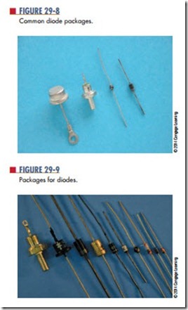
Once the P–N junction is formed, the diode must be packaged to protect it from both environmental and mechanical stresses. The package must also provide a means of connecting the diode to a circuit. Package style is determined by the purpose or application of the diode (Figure 29-8). If large currents are to flow through the diode, the package must be designed to keep the junction from overheating. Figure 29-9 shows the package for diodes rated at 3 A or less. A black, white, or silver band on the end identifies the cathode.
Questions
1. Describe three methods of diode fabrication.
2. Which method of diode fabrication is favored over the others?
3. Draw four common diode packages.
4. How is the cathode identified on diode packages rated at less than 3 A?
5. Why are the diodes after fabrication put in a package?
Related posts:
Incoming search terms:
- diode construction techniques
- grown junction method
- grown junction
- diffused junction diode
- growth junction method
- Pn junction fabrication
- method of formation of pn junction
- melt grown junctions method
- methods of formation of pn junction
- method used to fabricate PN junction
- fabrication of pn junction
- methods of p-n junction formation
- junction method
- Technique of febrication of pn junction ditail
- Alloying method for formation of pn junction
- method of construction to pn junction diode
- methods of forming pn junction
- fabircation of pn junction grown junction method
- formation of p-n junction using defusion technology
- melt grown junction method
- grown junction diode
- grown junction method of pn diode
- aloying method of pn junction
- grown junction p-n junction
- grown junc
- growing methods p-n junction
- formation of pn junction by alloying
- formation of pn junction by grown junction method
- growing method of pn junction
- Grown junction method when forming a pn junction
- grown junction method of pn junction fabrication
- Diffused junction medthod
- explain the types of pn junction fabrication techniques
- why diode put in packages after fabrication
- alloying process of diodes
- construction of I -V characteristics of pn junction
- CONSTRUCTION OF JUNCTION DIODE
- construction of pn junction diode
- construction techniques of doide
- define grown junction diode
- Describe the three methods of diode fabrication Illustrate with diagrams Which method of diode fabrication is favored over the others and why?
- diffused junction method of making diode
- diffusing method growing method and alloying method are also used to form p-n junction
- diffusing method of pn juntion
- diffusing method pn junction
- diffusion junction technique
- diode construction technique
- diode fabrication technique
- diode fbrication
- explain growth junction method of fabrication
