It is difficult to convince people that this frequency is of no relevance whatsoever to the speed of amplifiers and that it does not affect the slew rate. Nonetheless, it is so, and any first-year electronics textbook will confirm this. High-gain op-amps with sub-1-Hz bandwidths and blindingly fast slewing are as common as the grass (if somewhat less expensive) and if that does not demonstrate the point beyond doubt then I really do not know what will.
Limited open-loop bandwidth prevents the feedback signal from immediately following the system input, so the utility of this delayed feedback is limited. No linear circuit can introduce a pure time delay; the output must begin to respond at once, even if it takes a long time to complete its response. In the typical amplifier the dominant-pole capacitor introduces a 90° phase shift between input pair and output at all but the lowest audio frequencies, but this is not a true time delay. The phrase delayed feedback is often used to describe this situation, and it is a wretchedly inaccurate term; if you really delay the feedback to a power amplifier (which can only be done by adding a time constant to the feedback network rather than the forward path) it will quickly turn into the proverbial power oscillator as sure as night follows day.
Amplifier Stability and Negative Feedback
In controlling amplifier distortion, there are two main weapons. The first is to make the linearity of the circuitry as good as possible before closing the feedback loop. This is unquestionably important, but it could be argued that it can only be taken so far before the complexity of the various amplifier stages involved becomes awkward. The second is to apply as much negative feedback (NFB) as possible while maintaining amplifier stability. It is well known that an amplifier with a single time constant is always stable, no matter how high the feedback factor. The linearization of the VAS by local Miller feedback is a good example. However, more complex circuitry, such as the generic three-stage power amplifier, has more than one time constant, and these extra poles will cause poor transient response or instability if a high feedback factor is maintained up to the higher frequencies where they start to take effect. It is therefore clear that if these higher poles can be eliminated or moved upward in frequency, more feedback can be applied and distortion will be less for the same stability margins. Before they can be altered—if indeed this is practical at all—they must be found and their impact assessed.
The dominant pole frequency of an amplifier is, in principle, easy to calculate; the mathematics are very simple. In practice, two of the most important factors, the effective beta of the VAS and the VAS collector impedance, are only known approximately, so the dominant pole frequency is a rather uncertain thing. Fortunately, this parameter in itself has no effect on amplifier stability. What matters is the amount of feedback at high frequencies.
Things are different with the higher poles. To begin with, where are they? They are caused by internal transistor capacitances and so on, so there is no physical component to show where the roll-off is. It is generally regarded as fact that the next poles occur in the output stage, which use power devices that are slow compared with small-signal transistors. Taking the Class-B design, the TO-92 MPSA06 devices have an Ft of 100 MHz, the MJE340 drivers about 15 MHz (for some reason this parameter is missing from the data sheet), and the MJ802 output devices an Ft of 2.0 MHz. Clearly the output stage is the prime suspect. The next question is at what frequencies these poles exist. There is no reason to suspect that each transistor can be modeled by one simple pole.
There is a huge body of knowledge devoted to the art of keeping feedback loops stable while optimizing their accuracy; this is called control theory, and any technical bookshop will yield some intimidatingly fat volumes called things like “control system design.” Inside, system stability is tackled by Laplace-domain analysis, eigenmatrix methods, and joys such as the Lyapunov stability criterion. I think that makes it clear that you need to be pretty good at mathematics to appreciate this kind of approach.
Even so, it is puzzling that there seems to have been so little application of control theory to audio amplifier design. The reason may be that so much control theory assumes that you know fairly accurately the characteristics of what you are trying to control, especially in terms of poles and zeros.
One approach to appreciating NFB and its stability problems is SPICE simulation. Some SPICE simulators have the ability to work in the Laplace or s-domain, but my own experiences with this have been deeply unhappy. Otherwise respectable simulator packages output complete rubbish in this mode. Quite what the issues are here I do not know, but it does seem that s-domain methods are best avoided. The approach suggested here instead models poles directly as poles, using RC networks to generate the time constants. This requires minimal mathematics and is far more robust. Almost any SPICE simulator, evaluation versions included, should be able to handle the simple circuit used here.
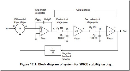
Figure 12.1 shows the basic model, with SPICE node numbers. The scheme is to idealize the situation enough to highlight the basic issues and exclude distractions such as nonlinearities or clipping. The forward gain is simply the transconductance of the input stage multiplied by the transadmittance of the VAS integrator. An important point is that with correct parameter values, the current from the input stage is realistic, as are all the voltages.
The input differential amplifier is represented by G. This is a standard SPICE element—the VCIS, or voltage-controlled current source. It is inherently differential, as the output current from Node 4 is the scaled difference between the voltages at Nodes 3 and 7. The scaling factor of 0.009 sets the input stage transconductance (gm) to 9 mA/V, a typical
figure for a bipolar input with some local feedback. Stability in an amplifier depends on the amount of NFB available at 20 kHz. This is set at the design stage by choosing the input gm and Cdom, which are the only two factors affecting the open-loop gain. In simulation it would be equally valid to change gm instead; however, in real life it is easier to alter Cdom as the only other parameter this affects is slew rate. Changing input stage transconductance is likely to mean altering the standing current and the amount of local feedback, which will in turn impact input stage linearity.
The VAS with its dominant pole is modeled by the integrator Evas, which is given a high but finite open-loop gain, so there really is a dominant pole P1 created when the gain demanded becomes equal to that available. With Cdom = 100 pF, this is below 1 Hz.
With infinite (or as near-infinite as SPICE allows) open-loop gain, the stage would be a perfect integrator. As explained elsewhere, the amount of open-loop gain available in real versions of this stage is not a well-controlled quantity, and P1 is liable to wander about in the 1- to 100-Hz region; fortunately, this has no effect at all on HF stability. Cdom is the Miller capacitor that defines the transadmittance, and since the input stage has a realistic transconductance, Cdom can be set to 100 pF, its usual real-life value. Even with this simple model we have a nested feedback loop. This apparent complication here has little effect, as long as the open-loop gain of the VAS is kept high.
The output stage is modeled as a unity-gain buffer, to which we add extra poles modeled by R1, C1 and R2, C2. Eout1 is a unity-gain buffer internal to the output stage model, added so that the second pole does not load the first. The second buffer Eout2 is not strictly necessary as no real loads are being driven, but it is convenient if extra complications are introduced later. Both are shown here as a part of the output stage but the first pole could equally well be due to input stage limitations instead; the order in which the poles are connected makes no difference to the final output. Strictly speaking, it would be more accurate to give the output stage a gain of 0.95, but this is so small a factor that it can be ignored.
The component values here are of course completely unrealistic and chosen purely to make the math simple. It is easy to appreciate that 1 Ω and 1 μF make up a 1-μs time constant. This is a pole at 159 kHz. Remember that the voltages in the latter half of the circuit are realistic, but the currents most certainly are not.
The feedback network is represented simply by scaling the output as it is fed back to the input stage. The closed-loop gain is set to 23 times, which is representative of most power amplifiers.
Note that this is strictly a linear model, so that the slew-rate limiting associated with Miller compensation is not modeled here. It would be done by placing limits on the amount of current that can flow in and out of the input stage.
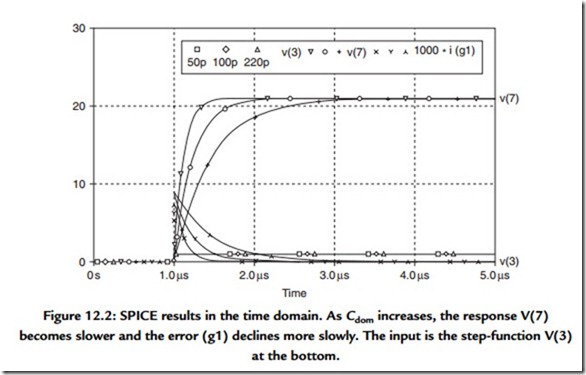
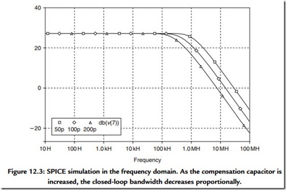
Figure 12.2 shows the response to a 1-V step input, with the dominant pole the only time element in the circuit. (The other poles are disabled by making C1, C2 0.00001 pF, because this is quicker than changing the actual circuit.) The output is an exponential rise to an asymptote of 23 V, which is exactly what elementary theory predicts. The exponential shape comes from the way that the error signal that drives the integrator becomes less as the output approaches the desired level. The error, in the shape of the output current from G, is the smaller signal shown; it has been multiplied by 1000 to get mA onto the same scale as volts. The speed of response is inversely proportional to the size of Cdom and is shown here for values of 50 and 220 pF as well as the standard 100 pF. This simulation technique works well in the frequency domain, as well as the time domain. Simply tell SPICE to run an AC simulation instead of a TRANS (transient) simulation. The frequency response in Figure 12.3 exploits this to show how the closed-loop gain in an
NFB amplifier depends on the open-loop gain available. Once more elementary feedback theory is brought to life. The value of Cdom controls the bandwidth, and it can be seen that the values used in the simulation do not give a very extended response compared with a 20-kHz audio bandwidth.
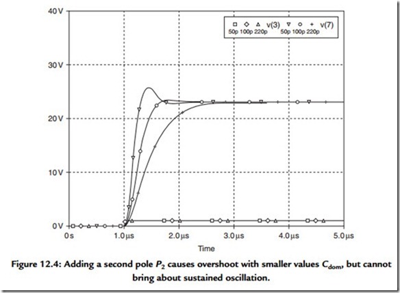
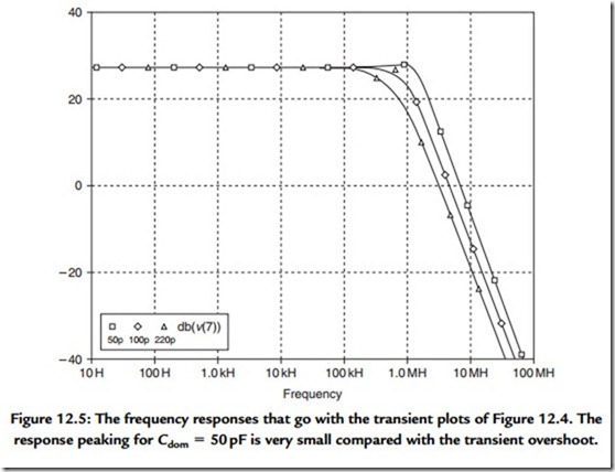
In Figure 12.4, one extra pole P2 at 1.59 MHz (a time constant of only 100 ns) is added to the output stage, and Cdom stepped through 50, 100, and 200 pF as before. 100 pF shows a slight overshoot that was not there before; with 50 pF there is a serious overshoot that does not bode well for the frequency response. Actually, it’s not that bad; Figure 12.5 returns to the frequency-response domain to show that an apparently vicious overshoot is actually associated with a very mild peaking in the frequency domain.
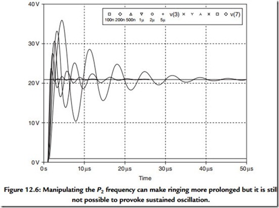
From here on Cdom is left set to 100 pF, which is its real value in most cases. In Figure 12.6, P2 is stepped instead, increasing from 100 ns to 5 μs, and while the response gets slower and shows more overshoot, the system does not become unstable. The reason is simple: sustained oscillation (as opposed to transient ringing) in a feedback loop requires
positive feedback, which means that a total phase shift of 180° must have accumulated in the forward path and reversed the phase of the feedback connection. With only two poles in a system the phase shift cannot reach 180°. The VAS integrator gives a dependable 90° phase shift above P1, being an integrator, but P2 is instead a simple lag and can only give a 90° phase lag at infinite frequency. So, even this very simple model gives some insight. Real amplifiers do oscillate if Cdom is too small, so we know that the frequency response of the output stage cannot be modeled meaningfully with one simple lag.
A certain president of the United States is alleged to have said: “Two wrongs don’t make a right—so let’s see if three will do it.” Adding in a third pole, P3, in the shape of another simple lag gives the possibility of sustained oscillation.
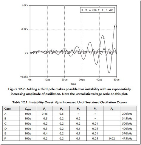
Stepping the value of P2 from 0.1 to 5 μs with P3 = 500 ns shows sustained oscillation starting to occur at P2 = 0.45 μs. For values such as P2 = 0.2 μs, the system is stable
and shows only damped oscillation. Figure 12.7 shows over 50 μs what happens when the amplifier is made very unstable (there are degrees of this) by setting P2 = 5 μs and P3 = 500 ns. It still takes time for the oscillation to develop, but exponentially diverging oscillation like this is a sure sign of disaster. Even in the short time examined here the amplitude has exceeded a rather theoretical half a kilovolt. In reality, oscillation cannot increase indefinitely, if only because the supply rail voltages would limit the amplitude.
In practice, slew rate limiting is probably the major controlling factor in the amplitude of high-frequency oscillation.
We have now modeled a system that will show instability. But does it do it right? Sadly, no. The oscillation is about 200 kHz, which is a rather lower frequency than is usually seen when an amplifier misbehaves. This low frequency stems from the low P2 frequency we have to use to provoke oscillation; apart from anything else this seems out of line with the
known Ft of power transistors. Practical amplifiers are likely to take off at around 500 kHz to 1 MHz when Cdom is reduced, which seems to suggest that a phase shift is accumulating quickly at this sort of frequency. One possible explanation is that there are a large number of poles close together at a relatively high frequency.
A fourth pole can be simply added to Figure 12.1 by inserting another RC–buffer combination into the system. With P2 = 0.5μs and P3 = P4 = 0.2μs, instability occurs at 345kHz, which is a step toward a realistic frequency of oscillation. This is case B in Table 12.1.
When a fifth output stage pole is grafted on, so that P3 = P4 = P5 = 0.2 μs, the system just oscillates at 500 kHz with P2 set to 0.01 μs. This takes us close to a realistic frequency of oscillation. Rearranging the order of poles so that P2 = P3 = P4 = 0.2 μs, while
P5 = 0.01 μs, is tidier and the stability results are of course the same; this is a linear system so the order does not matter. This is case C in Table 12.1.
Having P2, P3, and P4 all at the same frequency does not seem very plausible in physical terms, so case D shows what happens when the five poles are staggered in frequency. P2 needs to be increased to 0.3 μs to start the oscillation, which is now at 400 kHz. Case E is another version with five poles, showing that if P5 is reduced, P2 needs to be doubled to 04 μs for instability to begin.
In the final case F, a sixth pole is added to see if this permitted sustained oscillation is above 500 kHz. This seems not to be the case; the highest frequency that could be obtained after a lot of pole twiddling was 475 kHz. This makes it clear that this model is of limited accuracy (as indeed are all models—it is a matter of degree) at high frequencies and that further refinement is required to gain further insight.
Related posts:
Incoming search terms:
- effect of current shunt NFB on voltage gain
- effect of negative feedback on stability
- effect of negative feedback on phase lag
- How does negative feedback amplifier increases distortion
- negative feedback and effect of it on bandwoth and stability
- gain stability negative feedback
- gain stability in negative feedback
- effect of negative feedback on the stability
- effect of negative feedback on phase shift of amplifier
- Effect of negative feedback
- stability of negative feedback amplifier
