In the course of this book several circuit methods have been described, and this chapter is a summary of these methods that apply to instrumentation together with a longer description of the methods that are used for analogue to digital (A-D) and digital to analogue (D-A) conversion. Of these, the A-D and D-A methods are the more important because the rate of develop- ment of these methods has been rapid and many readers will not be familiar with the current state of the methods that are used. For that reason, the more familiar methods are presented in summary form, but the D-A and A-D conversions are described in detail from first principles. In particular, although many texts describe methods that are applicable to DC or low-frequency analogue conversion, few deal with the methods that have to be used for wide amplitude and frequency ranges.
The main non-digital instrumentation methods can be grouped as impedance converters, bridge circuits and operational amplifiers. Of these, the impedance converters are mainly the familiar emitter-follower and source-follower circuits. The use of a MOSFET as a source-follower has largely replaced the older techniques using electrometer valves for very high input impedance applications, although electrometer valves are still used in some equipment for insulation testing. Bridge circuits have been covered as required in this book, and the only linear method that requires more detailed description is the use of operational IC amplifiers.
Op-amps
For most purposes, an IC of the type called the operational amplifier (usually shortened to op-amp) will be used in place of a multi-stage amplifier constructed from individual transistors. The internal circuit of
such an IC is not necessarily known to the user, and the important point to recognize is that the gain and other features of the op-amp will be set by external components such as resistors. This is true also of most amplifiers that have been constructed by using individual transistors, but since the op-amp consists of one single component, it is very much easier to see which components control its action, since only these components are visible on the circuit board. In many applications, only one or two resistors will be required to be of close tolerance.
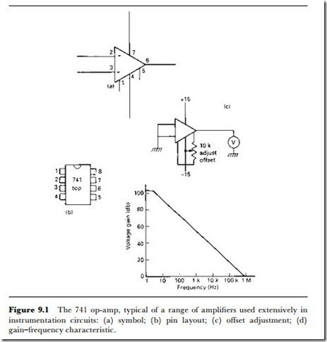
The ‘typical’ op-amp is the type 741, which is a very old design of bipolar op-amp but one whose basic principles are followed by most of the modern types also. Figure 9.1 shows the connections to, and the symbol for, an op- amp of this type – the triangular symbol is used for any op-amp, but some of the connections are not used for modern op-amp types. The important point to note is that the op-amp has two signal inputs, marked with + and
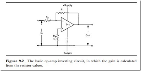
– signs. A signal at the + input will appear amplified at the output and in phase. A signal at the – input will also appear amplified at the output, with the same figure of gain, but inverted. If the same signal is applied to each input the output should be zero, because the action of the op-amp is to amplify the difference between the signals at its two inputs. If both inputs are used in this way, the amplifier is acting as a differential amplifier. For many purposes, however, the op-amp is used single-ended, meaning that only one input signal is supplied consisting of a voltage whose amplitude varies with respect to ground. For such a signal, the op-amp can be used in two ways – as an inverting amplifier or as a non-inverting amplifier. The gain of the op-amp in its natural state is very high, of the order of 100 dB, equivalent to a voltage gain of 100 000 times, so that for almost all practical uses this gain has to be reduced by using negative feedback. The negative feedback connection is from the output terminal to the (-) input. If we simply connect a resistor from the output to the (-) input, the negative feedback is 100% – all of the output voltage signal is connected back to the input, and the gain will be unity. We need to be able to take a signal to the input, however, and if we want the output signal to be inverted relative to the input, the signal input has to be to the (-) terminal. Connecting the input signal by way of a resistor (Figure 9.2) will reduce the amount of negative feedback, and so permit the gain to be greater than unity if required. In the circuit of Figure 9.2, the voltage gain is given by R1/R2 (in decibels, 20 log [R1/R2]). To achieve unity gain, we can make these resistor values equal, and by using different values we can achieve various figures of voltage gain. The value of R2 includes any circuit resistance of the source of the signal, and more easily predictable results are obtained if this resistor is of several k1 in value, swamping source resistance values.
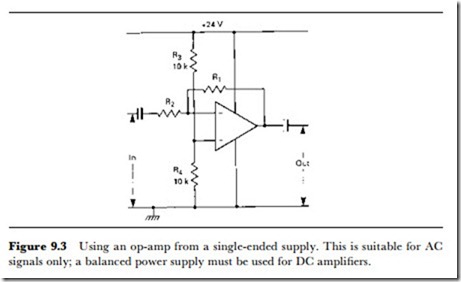
The DC bias of the op-amp is achieved most simply by using two supplies of equal positive and negative voltages, typically +12 V and -12 V. When
this is done, provided that there is a resistor of not too high a value connect- ing the output with the (-) input, the op-amp will be correctly biased. If it is inconvenient to have to supply voltages like this, the circuit can be re- arranged to the type shown in Figure 9.3, using a single voltage supply. In this case, however, capacitors are needed to isolate the DC voltages. The DC voltage on the (+) input is set to half of the supply voltage by using resistors R3 and R4 of equal value, but the remainder of the circuit is con- structed in the same way as before, with capacitors now used to feed signals in and out. The DC level of both input and output will be approxi- mately half of the supply voltage.
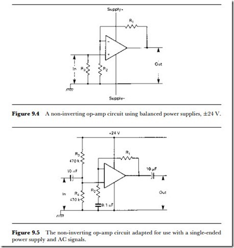
The inverting amplifier connection of the op-amp is used to a large extent, but for some purposes a non-inverting connection can be useful. The amplifier is non-inverting if the signal is taken to the (+) input, but the feedback must still be connected to the (-) input, and the amount of feedback will decide how much gain is obtained. Figure 9.4 illustrates a typical non-inverting circuit, using balanced + and – power supplies. The voltage gain is now equal to (R1 + R2)/R2, so that if unity gain is needed, the resistor R2 should be omitted. The input of signal is taken to the (+) input terminal, with a resistor connected to ground to ensure correct DC conditions as usual. The input resistance of the op-amp is very high, but the use of R3 makes the value equal approximately to the size of this resistor. The output resistance, as always, is low – a few ohms. The version of this circuit for a single-ended power supply is illustrated in Figure 9.5.
SLEW AND BANDWIDTH
The use of op-amps does not solve all the problems of providing gain,
although for low-frequency signals there are few problems to overcome. Because the op-amp is a very complicated circuit that makes use of many transistors in common-emitter circuits, its gain for high-frequency signals will be lower than its gain for low-frequency signals. More seriously, its gain for large-amplitude fast-changing signals will be lower than for low- amplitude signals of the same frequency. This latter problem is one of slew rate.
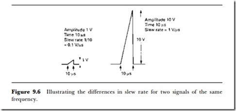
The slew rate of a signal is the rate of change of voltage in the signal, in terms of V/s. In practice, this gives figures that are much too large, and the more practical unit of V/f.s is used. The importance of slew rate is that two waves of identical frequency and waveshape can have very different slew rates, depending on their peak amplitudes. Suppose, for example that we have a wave that is of sawtooth shape and which repeats at 100 kHz. It is
easy to design an op-amp circuit that will provide a large figure of voltage gain for a wave with this frequency, but the slew rate also has to be considered, as Figure 9.6 shows. If the amplitude of the wave is 1 V, then for a time of 10 f.s (corresponding to a frequency of 100 kHz), the slew rate is 1V in 10 f.s, equal to 0.1 V/f.s. For a 10 V amplitude, however, the slew rate is 10 V/10 f.s, equal to 1 V/f.s. The amplifier must cope with the slew rate of the highest amplitude of signal at the output. As it happens, many op-amps will cope with a slew rate of 1 V/f.s, but the 741 type is limited to a slew rate of 0.5 V/f.s. For higher slew rates, however, it may be necessary to specify different op-amps.
The maximum slew rate cannot be altered by circuit tricks such as negative feedback; it is fixed by the internal design of the op-amp itself. Unlike the bandwidth for small sine wave signals, which can be increased by using more negative feedback and sacrificing gain, slew rate is a fundamental figure for the op-amp. High slew-rate op-amps can be obtained for applications in which this figure must be large. To take an example, the RS 5539 op-amp has a quoted slew rate of 600 V/f.s, making this op-amp suitable for very fast-changing signals, including sine waves approaching the 1 GHz range. This, however, is exceptional, and slew rate figures in the range 0.5-10 V/f.s are more common.
The slew rate is a very useful figure to use when an op-amp is employed in circuits that use sawtooth, pulse and other non-sine waveshapes. For sine wave use, an alternative figure – the power bandwidth – is more useful. The power bandwidth is the maximum frequency of signal that can be amplified at full power. If higher frequencies are used, lower gains must be used so that the product of gain in decibels and frequency in (usually) MHz or kHz is the same. In other words, if the gain of an op-amp is quoted as 100 dB (gain of 100 000 times) and its power bandwidth as 10 kHz, you can expect to be able to use the full 100 dB of gain on signals up to 10 kHz, and if you make the gain 10 000 (80 dB) you can use signal frequencies up to 100 kHz, and so on. To put it another way, each 20 dB reduction of gain (by using negative feedback) will give a 10-fold rise in maximum operating frequency.
This, however, is still subject to the slew rate limitation, so that the slew rate should always be calculated first. For a sine wave, the slew rate in V/ f.s is given by 6.3 x Vo x f , where Vo is the peak amplitude, and f is the frequency in MHz. For example, a sine wave of 5 V peak and 0.5 MHz frequency would have a slew rate of 6.3 x 5 x 0.5 = 15.75 V/f.s. Only a limited number of op-amp types can cope with this slew rate, although many could give the required bandwidth for signals of lower amplitudes.
CDA AND TRANSCONDUCTANCE AMPLIFIERS
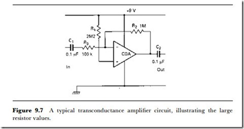
Another type of op-amp that is used for some purposes is the current-difference amplifier (CDA), otherwise known as a Norton amplifier. In an amplifier of this type, the output voltage is proportional to the difference between the currents at the two inputs. This leads to circuits that look very odd when compared with the usual type of op-amp, because the input currents are set with the aid of large-value resistors, as Figure 9.7 illustrates. The current to the ‘+’ input is set with a 2M2 resistor, and since the voltage at the output is normally required to be about half of the supply voltage, a 1M resistor from this point to the ‘-‘ input will set the bias current correctly. The advantage of using a CDA is that the voltage swing at the output can be very close to the limits of the supply voltage, making this type of amplifier useful in interfaces to digital equipment.
Another comparatively rare type of op-amp is the transconductance amplifier, in which the transconductance (milliamps of current output per voltage difference between the inputs) can be chosen by setting the bias current. Such amplifiers are used in gain-controlled circuits.
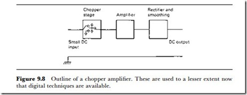
An alternative to the use of operational amplifiers is the chopper amplifier. The principle is illustrated in Figure 9.8, and is used to attain very high-gain DC amplification. A low-amplitude DC signal is converted into a square wave by ‘chopping’ the signal on and off, using FET switches, and using this square wave as the input to a pulse amplifier. Very high gain of such a waveform can be obtained, and the output square wave can be rectified and smoothed to obtain a high-level DC signal whose amplitude will be very precisely proportional to the amplitude of the original signal. Chopper amplifiers are less liable to drift than direct- coupled DC amplifiers and chopping techniques can also be applied to more conventional op-amps in order to reduce offset. See also Chapter 12 for chopper principles.
