Enhancement Insulated Gate FETs (MOSFETs)
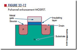
Depletion MOSFETs are devices that are normally on. That is, they conduct a substantial amount of drain cur- rent when the gate-to-source voltage is 0. This is useful in many applications. It is also useful to have a device that is normally off—that is, a device that conducts only when a suitable value of EGS is applied. Figure 32-12 shows a MOSFET that functions as a normally off de- vice. It is similar to a depletion MOSFET, but it does not have a conducting channel. Instead, the source and drain regions are diffused separately into the substrate. The figure shows an N-type substrate and P-type source and drain regions. The opposite arrangement could also be used. The lead arrangements are the same as with a depletion MOSFET.
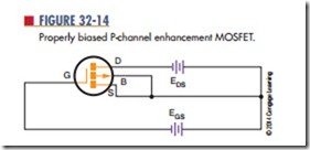
A P–channel enhancement MOSFET must be biased so that the drain is negative with respect to
the MOSFET’s drain negative with respect to the source. EGS also makes the gate negative with respect to the source. Only when EGS increases from 0 volts the source. When only the drain-to-source voltage (EDS) is applied, a drain current does not flow. This is because there is no conducting channel between the source and drain. When the gate is made negative with respect to the source, holes are drawn toward the gate, where they gather to create a P-type channel that allows current to flow from the drain to the source. When the negative gate voltage is increased, the size of the channel increases, allowing even more current to flow. An increase in gate voltage tends to enhance the drain current.
The gate of a P-channel enhancement MOSFET can be made positive with respect to the source without affecting the operation. The MOSFET’s drain current is 0 and cannot be reduced with the application of a positive gate voltage.
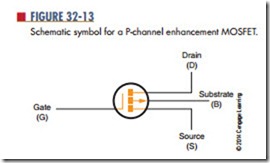
The schematic symbol for a P-channel enhancement MOSFET is shown in Figure 32-13. It is the same as that for a P-channel depletion MOSFET except that a broken line is used to interconnect the source, drain, condition. The arrow points outward to indicate a A properly biased P-channel enhancement MOSFET and applies a negative voltage to the gate does a substantial amount of drain current flow. The substrate is normally connected to the source, but in special applications the substrate and source may be at different potentials.
N-channel enhancement MOSFETs may also be constructed. These devices operate with a posi- tive gate voltage so that electrons are attracted toward the gate to form an N-type channel. Otherwise, these devices function like P-channel devices.
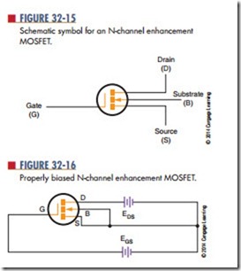
Figure 32-15 shows the schematic symbol for an N-channel enhancement MOSFET. It is similar to the P-channel device except that the arrow points inward to identify the N channel. Figure 32-16 shows a prop- erly biased N-channel enhancement MOSFET.
MOSFETs are usually symmetrical, like JFETs. Therefore, the source and drain can usually be reversed or interchanged.
QUESTIONS
1. How do depletion and enhancement MOSFETs differ from each other?
2. Describe how an enhancement insulated gate FET operates.
3. Draw and label the schematic symbols for P-channel and N-channel enhancement MOSFETs.
4. Why are there four leads on a MOSFET?
What leads on an enhancement MOSFET can be reversed?


