JUNCTION FETs
The junction field effect transistor (JFET) is a unipolar transistor that functions using only majority carriers. The JFET is a voltage-operated device. JFETs are constructed from N-type and P-type semiconductor materials and are capable of amplifying electronic signals, but they are constructed differently from bipolar transistors and operate on different principles. Knowing how a JFET is constructed helps to understand how it operates.
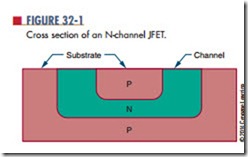
Construction of a JFET begins with a substrate, or base, of lightly doped semiconductor material. The substrate can be either P- or N-type mate- rial. The P–N junction in the substrate is made using both the growth and diffusion methods (see Chap- ter 29). The shape of the P–N junction is important. Figure 32-1 shows a cross section of the embedded region within the substrate. The U-shaped region is called the channel and is flush with the upper surface of the substrate. When the channel is made of N-type material in a P-type substrate, an N-channel JFET is formed. When the channel is made of P-type material in an N-type substrate, a P-channel JFET is formed.
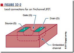
Three electrical connections are made to a JFET (Figure 32-2). One lead is connected to the substrate to form the gate (G). One lead is connected to each end of the channel to form the source (S) and the drain (D). It does not matter which lead is attached to the source or drain, because the channel is symmetrical.
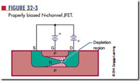
The operation of a JFET requires two external bias voltages. One of the voltage sources (EDS) is connected between the source and the drain, forcing the current to flow through the channel. The other voltage source (EGS) is connected between the gate and the source. It controls the amount of current flowing through the channel. Figure 32-3 shows a properly biased N-channel JFET.
Voltage source EDS is connected so that the source is made negative with respect to the drain. This causes a current to flow, because the majority carriers are electrons in the N-type material. The source-to-drain current is called the FET’s drain current (ID). The channel serves as resistance to the supply voltage (EDS).
The gate-to-source voltage (EGS) is connected so that the gate is negative with respect to the source.
This causes the P–N junction formed by the gate and channel to be reverse biased. This creates a depletion region in the vicinity of the P–N junction, which spreads inward along the length of the channel. The depletion region is wider at the drain end because the EDS voltage adds to the EGS voltage, creating a higher- reverse bias voltage than that appearing across the source end.
The size of the depletion region is controlled by EGS. As EGS increases, so does the depletion region. A decrease in EGS causes a decrease in the depletion region. When the depletion region increases, it effectively reduces the size of the channel, which in turn reduces the amount of current that is able to flow through it. EGS can thus be used to control the drain current (ID) that flows through the channel. An increase in EGS causes a decrease in ID.
In normal operation, the input voltage is applied between the gate and the source. The resulting output current is the drain current (ID). In a JFET, the input voltage is used to control the output current. In a transistor, it is the input current, not the voltage, which is Because the gate-to-source voltage is reverse biased, the JFET has an extremely high input resistance. If the gate-to-source voltage were forward biased, a large current would flow through the channel, causing the input resistance to drop and reducing the gain of the device. The amount of gate-to-source voltage required to reduce ID to zero is called the gate–to–source
cutoff voltage (EGS(off)). The manufacturer of the device specifies this value.
The drain–to–source voltage (EDS) has control over the depletion region within the JFET. As EDS increases, ID also increases. A point is then reached where ID levels off, increasing only slightly as EDS continues to rise. This occurs because the size of the depletion
region has increased also, to the point where the channel is depleted of minority carriers and cannot allow ID to increase proportionally with EDS. The resistance of the channel also increases with an increase of EDS, with the result that ID increases at a slower rate. However, ID levels off because the depletion region expands and re- duces the channel’s width. When this occurs, ID is said to pinch off. The value of EDS required to pinch off, or limit, ID is called the pinch-off voltage (EP). The manufacturer usually gives the EP for an EGS of 0. EP is always close to EGS(off) when EGS is equal to 0. When EP is equal to EGS, the drain current is pinched off.
P-channel and N-channel JFETs have the same char- acteristics. The main difference between them is the di- rection of the drain current (ID) through the channel. In a P-channel JFET, the polarity of the bias voltages (EGS, EDS) is opposite to that in an N-channel JFET.
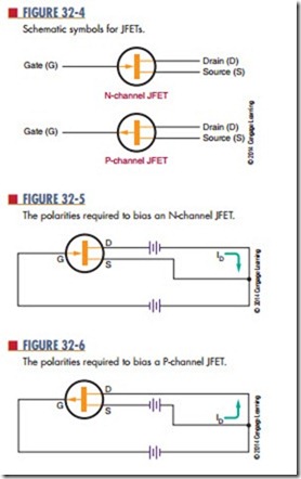
The schematic symbols used for N-channel and P-channel JFETs are shown in Figure 32-4. The polari- ties required to bias an N-channel JFET are shown in Figure 32-5 and for a P-channel JFET in Figure 32-6.
QUESTIONS
1. Describe how a JFET differs in construction from a bipolar transistor.
2. Identify the three electrical connections to the JFET.
3. How is the current shut off in a JFET?
4. Define the following with reference to JFETs:
a. Depletion region
b. Pinch-off voltage
c. Source
d. Drain
5. Draw and label schematic diagrams of P-channel and N-channel JFETs.


