POWER SUPPLIES
The common denominator of all transistor circuits is the dc power supply. Some circuits require higher voltages or a greater current supply, but all transistors require dc power to function. It can be said that the power supply provides the “life blood” for any equipment. In addition to the basic requirement of providing a suitable supply for operating transistor circuits and integrated circuits, consideration of the design of power supplies includes several other aspects, such as the use of diodes and transistors in voltage stabilising circuits.
Considerable developments have taken place in the design of voltage stabilising circuits, and it is significant that these stabilising circuits, form an important application of a transistor, not only for stabilised supplies for transistor circuits but also to provide constant and reference voltages for many other items of electronic equipment. The various aspects of power supplies are covered in this chapter, with emphasis on the use of transistors in stabilising circuits.
RECTIFIER CIRCUITS
There are various standard rectifier circuits, the choice depending upon the required dc voltage and load current and on economic considerations coupled with the required reliability. Since the voltage required for transistor circuits is normally low, in the range of 10–100 volts, a step-down mains transformer will generally be used.
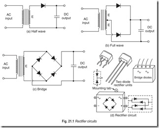
(1) Half-wave Rectifier Circuit: Half-wave rectifier circuit is the simplest rectifier circuit and is shown in Fig 21.1 (a). If the rms voltage of the transformer secondary is E, the dc voltage across the reservoir capacitor will be ![]() E with no load, falling to approximately E at full load, depending upon the value of the capacitor. During the non-conducting half-cycle, the peak inverse voltage appearing across the rectifier will be the sum of the peak values of the ac input voltage and the voltage across the capacitor. This can have a maximum value of
E with no load, falling to approximately E at full load, depending upon the value of the capacitor. During the non-conducting half-cycle, the peak inverse voltage appearing across the rectifier will be the sum of the peak values of the ac input voltage and the voltage across the capacitor. This can have a maximum value of ![]() E. The dc ripple appearing on the dc output will have a frequency equal to the mains frequency. The ripple output of the half-wave rectifier is more difficult to smooth, however, because a pulsation of current occurs only once in each cycle of the 50 Hz current, it is charged twice as often.
E. The dc ripple appearing on the dc output will have a frequency equal to the mains frequency. The ripple output of the half-wave rectifier is more difficult to smooth, however, because a pulsation of current occurs only once in each cycle of the 50 Hz current, it is charged twice as often.
(2) Full-wave Rectifier Circuit: The full-wave rectifier circuit is illustrated in Fig. 21.1 (b). A centre- tapped secondary winding is used with two rectifiers connected so that each uses one half of the ac input. One rectifier delivers current to the load during the “odd” half-cycles and the other during the “even” half- cycles. If E is the rms ac voltage across each half of the secondary winding the dc output voltage across the capacitor will again be ![]() E with no load, but will only fall to the order of 1.2E on load, since the second rectifier helps to hold the voltage up. As there are two rectifiers supplying current to the load, each rectifier will only be passing one half of that passed by the single rectifier in the half-wave case. The ripple on the dc output voltage will be twice that of the mains frequency. The output of a full-wave rectifier is easier to smooth as compared to the output of a half-wave rectifier. The chief disadvantage of the full-wave rectifier system is that the transformer must have a centre-tapped secondary winding.
E with no load, but will only fall to the order of 1.2E on load, since the second rectifier helps to hold the voltage up. As there are two rectifiers supplying current to the load, each rectifier will only be passing one half of that passed by the single rectifier in the half-wave case. The ripple on the dc output voltage will be twice that of the mains frequency. The output of a full-wave rectifier is easier to smooth as compared to the output of a half-wave rectifier. The chief disadvantage of the full-wave rectifier system is that the transformer must have a centre-tapped secondary winding.
(3) Bridge Rectifier Circuit: The bridge rectifier circuit is shown in Fig. 21.1 (c). The use of this circuit gives full wave rectification without a centre-tapped winding. The peak inverse voltage appearing across the rectifiers is equal to the peak value of the ac input voltage, i.e. ![]() E. This is only one-half of the value with the previous full-wave circuit, and so for a given value of output voltage the rectifiers need have only half the voltage rating. To offset this, four rectifiers are needed instead of two. Typical bridge-rectifier diode packages are illustrated in Fig. 21.1 (d).
E. This is only one-half of the value with the previous full-wave circuit, and so for a given value of output voltage the rectifiers need have only half the voltage rating. To offset this, four rectifiers are needed instead of two. Typical bridge-rectifier diode packages are illustrated in Fig. 21.1 (d).
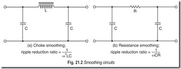
(4) Smoothing Circuits: The amplitude of the ripple voltage appearing on the dc output is reduced by including a low-pass filter consisting of an inductance–capacitance, or resistance–capacitance combination, as shown in Fig. 21.2. Filtering requirements are more stringent where very low signal levels are involved because of the ease with which ac ripple is picked up and combined with the desired signal.
The resistance smoothing element will, of course, introduce a higher drop in voltage than the inductance and will result in more severe regulation, and so normally is only used for low current, constant load applications.
Choke-input circuits are superior to capacitor–input types as long as current flows through the choke used for filtering. However, during times when no load is drawn from the source, the capacitor charges to the peak it would reach if the choke were not in the circuit, resulting in a higher overall swing than would exist with a capacitor input alone. Circuits using choke-input filters should be designed to cause current to flow through the choke at all times. Normally this can be achieved by using a resistive load in the power supply itself, particularly when the supply is not taxed during normal operation.
VOLTAGE REGULATION
Any change in “B+” supply voltage level may cause transistors to operate improperly. To stabilise the operating voltage, a voltage regulator circuit is used. As the load current taken from a normal rectifier circuit is increased the output voltage will fall, partly due to the ohmic resistance of the transformer windings, the rectifiers and the smoothing elements, and partly due to the lower effective storage efficiency of the reservoir capacitor with the lower load resistance. In many applications the load current will vary as, for example, in class B and switching circuits, and it is then desirable to include some form of stabilisation to maintain the output voltage constant. Various arrangements can be used depending upon the degree of stabilisation required.
The output voltage developed by any power supply tends to decrease when a current-drawing load is connected to it. The amount of change in the output voltage is usually expressed by a “per cent regulation”, and power supplies may be evaluated by comparing such quantitative values.
The difference between the no-load voltage and full-load voltage of a power supply is caused by the flow of load current through the internal resistance of the power supply. The voltage drop caused by the load current within the supply circuit is taken from the voltage available for the load resistance at the output terminals. An ideal power supply would have an internal impedance of zero and a per cent regulation of 100 (which could be expressed as per cent regulation required, or 0 per cent, because the output voltage would be precisely the same under full-load or no-load). In general, the lower the required per cent regulation, the better the supply for transistor and integrated circuit applications.
ZENER DIODE SHUNT STABILISER
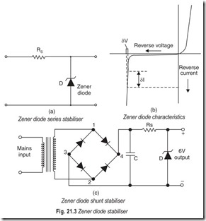
The zener diode stabiliser has the advantage of simplicity, and for many applications, particularly for low current loads, it can give sufficient stabilisation. The arrangement is shown in Fig. 21.3 (a). The zener diode is connected in the reverse direction across the load and is fed from the unstabilised voltage through a series resistor RS. The chracteristic of a zener diode is illustrated in Fig. 21.3 (b). In the reverse direction the current is small until the breakdown in reached, and then the current increases very rapidly for a small increase of voltage. The diode is chosen to have a breakdown voltage equal to the required output voltage, and the input voltage and series resistance are set so that the diode is biased in the breakdown region at a predetermined current such as the value I in Fig. 21.3 (b). Now if the load current increases the output voltage will tend to fall, but this will result in a decrease in the diode current such that the sum of the load plus diode currents remains almost constant. Thus the output voltage will remain almost constant, the only voltage change being dV due to the change in the diode current dI.
Similarly, if the input supply voltage increases, the voltage across the zener diode will tend to increase, causing an increased current through the zener diode. This extra current will produce a voltage drop across the series resistance RS almost equal to the increase of input voltage, thus keeping the output voltage almost constant.
At maximum load current and minimum input voltage there must still be sufficient current flowing through the zener diode to hold it in the breakdown region at least 2 or 3 mA. If this value is IM and the maximum load current IL , the total current flowing through the series resistance Rs will be (IM + ImL ). If the minimum input voltage is VM and the stabilised output voltage VO .
For good stabilisation the value of VM should preferably be at least 1.5 times the value of VO .
A practical example of a zener diode shunt stabiliser circuit is shown in Fig. 21.3 (c). This circuit gives an output voltage of 6 volts. It allows an input voltage variation of + 15 per cent and a load current variation of 5 to 50 mA with a maximum output voltage change of only 0.1 volt.
For higher output voltages, diodes with correspondingly high breakdown voltage can be used, but the value of the diode slope resistance in the breakdown region increases faster than the value of breakdown voltage, and better performance can be obtained by connecting two or more low-voltage (5–6 volts) zener diodes in series to obtain the required output voltage. This series arrangement also gives the optimum performance from the viewpoint of stability of the breakdown voltage with temperature changes as the change is nearly zero with diodes in the 5–6 volts region. The choice of method is entirely dependent upon the degree of stabilisation required and, of course, upon economic considerations.
TRANSISTOR SHUNT STABILISER
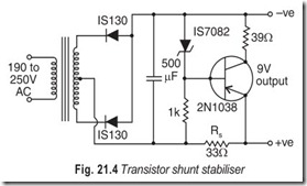
An improvement over the diode shunt stabiliser can be obtained with a transistor circuit as shown in Fig. 21.4. A transistor is connected across the supply, with its base electrode fed through a zener diode. The input voltage and base resistance are again set so that the zener diode is biased into the breakdown region. If the input voltage increases, the zener diode passes more current, which increases the base current of the transistor and causes a much larger current to flow down through the transistor. This increase of transistor current results in an increased voltage drop across the series resistance,RS, so that the output voltage is maintained almost at its original value.
The circuit shown in Fig. 21.4 was designed to give a stable 9 volts supply from the dc mains to replace the battery in portable transistor radio receivers. A mains voltage variation from 190 to 250 volts will result in an output voltage change of only 0.2 volt and a load current variation from 0 to 125 mA gives an output voltage change of 0.25 volt.
SERIES VOLTAGE STABILISER
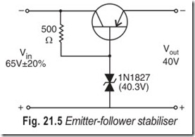
In series stabilising circuits it is arranged that the voltage change of an unstabilised supply appears across a series control transistor so that the output from the transistor remains constant. The simplest arrangement of this type of stabiliser is the emitter-follower circuit as shown in Fig. 21.5.
The base electrode of the transistor is held at a constant potential by means of the zener diode. The output voltage at the emitter of the transistor can only differ from this constant potential by an amount equal to the base-emitter voltage of the transistor, which is only a small fraction of 1 volt for germanium transistors, even over the full range of emitter current.
The excess voltage between the variable input voltage and the constant output voltage will appear across the collector and emitter of the transistor, and so it must be chosen to
have a sufficiently high collector voltage rating. Moreover, if the output emitter terminal is inadvertently shorted to earth, the full input voltage will appear across the transistor and if the collector voltage rating is not high enough to withstand this eventuality, some special protection circuit must be included.
The values given in Fig. 21.5 refer to an emitter follower stabiliser for 40 volts. A double-anode zener diode is used (sometime called a regulator diode). The circuit has the following performance characteristics:
Input voltage 52–78 volts
Output current 0–1.5 amperes
Output voltage 39.2–40.8 volts
Output impedance 0.3 W
FEEDBACK SERIES STABILISER
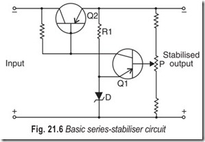
The operation of the simple emitter-follower circuit can be improved by including amplified feedback control
as shown in the base circuit of Fig. 21.6. A zener diode D is used as a constant voltage reference, beingbiased into the breakdown region through the reistance R1 . The diode holds the emitter of tansistor Q1 at the constant reference voltage. Any variation on the output voltage appears at the base of Q1, is amplified, and fed to the base of the series control transistor Q2, resulting in the collector-to-emitter voltage of Q2 changing to oppose the initial output variation.
Looking at the operation of the circuit in more detail, suppose the output voltage tends to increase either due to an increase in mains voltage or a decrease of load current. The percentage change in output voltage is fed to the base of the transistor Q1 by means of a potentiometer P across the output voltage. The level of the voltage applied to Q1 is approximately equal to the breakdown voltage of the zener diode connected to the emitter of the transistor. The voltageat the base of Q1 will go more negative and as the emitter is held constant by the diode D, the emitter-base voltage will
increase and cause the collector current of Q 1 to increase, and the collector to go more positive. This will reduce the emitter-base bias of the series control tansistor Q2 and result in an increase in collector-emitter voltage of that transistor, so that the output voltage is reduced back almost to the original level.
PRACTICAL POWER SUPPLY CIRCUITS
(1) 30 Volt,0.4 Ampere Stabiliser: A practical series stabiliser circuit for 30 volts, 400 mA output is shown in Fig 21.7. A 6.2 volt reference diode (D1) is used and the control element consists of a 2N1049 power transistor (actually a Darlington connected pair with a 2N656 transistor, this pair of transistors acts as a 2N1049 with very high gain). The circuit around Q4 and diode Q2 is called a pre-regulator circuit, and is included to provide a constant current to the collector of Q3 and the base of Q2. This circuit prevents any ripple existing on the input voltage from appearing at the base of Q2 and being amplified by the series transistor. The capacitor C is included to prevent high-frequency instability of the system.
For a change of input voltage of 35–70 volts, the output voltage change is 0.04 volt. For a change in output current from 0–400 mA, the output voltage change is 0.05 volt. For a change in ambient temperature from 0 to 75°C, the output voltage change is 0.2 volt.
(2) 50 Volt, 2.5 Ampere Stabilised Supply: A 50–volt stabilised supply suitable for use with a 20 watt amplifier is shown in Fig. 21.8. The stabiliser does not use a transistor pre-regulator as in the previous circuit. A resistance capacitance filter is used to reduce the ripple voltage at the base of the 2N1039 driver transistor. Two 12 volt zener diodes connected in series are used to give the reference voltage. The circuit is suitable for currents upto 2.5 amperes.
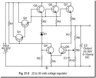
(3) 22 to 30 Volts Voltage Regulator: Fig. 21.9 shows a voltage regulator circuit providing an absolutely pure dc voltage from 22 to 30 volts, depending on the setting of potentiometer R 9. It uses a 12 volt zener diode as a reference, assuring line regulation of + 1% and load regulation within 0.5%. The circuit is designed for an input of 40–50 volts filtered dc.
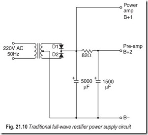
(4) Traditional Full-wave Rectifier Power Supply Circuit: A typical power supply for a receiver in the low-power class appears in Fig. 21.10. This is a simple two-diode full-wave rectifier circuit. It produces a much smoother form of pulsating dc than does the simpler half-wave rectifier circuit used in low-cost table model f.m. radios. Because of the higher ripple frequency less of the filtering network is required.
Notice the high value of the input filter capacitor. In solid state receivers, the value of this component ranges from 2,000 to 12,000 µF, depending on the design. Since dc voltage levels across these capacitors can approach 100 V in some receivers, extreme care must be exercised by service personnel. These sets are not portable transistor radios with the comparatively docile low voltage levels provided by batteries. In those sets we tend to get a little careless because we can touch anything in sight without any chance of injury.
In some modern solid-state stereo receivers, it is mandatory that we exercise the same degree of caution that we observe in older tube-type receivers.
In the power supply circuit in Fig. 21.10, a voltage dropping resistor and additional filtering are used to supply the power to some of the lower- level stages preceding the power amplifier. The second filter capacitor serves to decouple these stages from other receiver circuits and further suppress the ripple component.
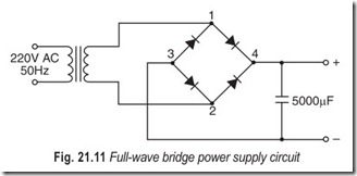
(5) Full-wave Bridge Power Supply Circuit: The power supply circuit shown in Fig. 21.11 is a full wave bridge circuit. Notice the absence of the centre tap on the power transformer secondary winding. This circuit has the ability to produce a dc output voltage that is roughly twice the output of the same transformer feeding a simple full-wave rectifier. This is because the bridge makes use of the entire secondary winding during each alternation, rather than just one half of the total winding. Of course, since a transformer cannot generate power, only converts what it receives, the bridge circuit also delivers one half the current capability of the two-diode full-wave system.
The bridge is probably the most popular power supply configuration in stereo receivers. It uses one pair of the four diodes in each half of the input sine wave. One pair of diodes is active on one alternation, while the other pair is active on the opposite alternation.
Diodes in the bridge connection are found in a variety of styles. In many receivers, the bridge is constructed of four separate and independent diode rectifiers. In others, you will find one of many available bridge connected four-diode packages. One common type of diode package is illustrated Fig. 21.1(d). This package is a thin square sandwich with the diodes mounted inside.
The terminals are marked with the “sine” symbol (~) for the ac connections and with “+” and “–” for the dc connections.
There are numerous other bridge rectifier stacks used in stereo receivers. In many instances it takes some imagination to identify certain imported rectifier stacks. In these cases, only the fact that the power transformer leads are attached to one set of terminals and the filter capacitor to the other set indicates that the component is a rectifier. In a few cases, there are only three leads attached to the bridge stack. In this situation you will notice that the stack is bolted to the common point or chassis. The bolt is the terminal for the negative side of the dc output. It remains grounded as long as the stack is bolted into place.
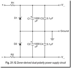
(6)Zener-derived Dual-polarity Power Supply Circuit: The circuit requiring a bipolar or dual-voltage power supply can be served by the configuration illustrated in Fig. 21.12 if the power-level demand is low enough. In this arrangement the dual-voltage characteristic is obtained from two series-connected zener diodes shunted across a normal monopolar power supply. The junction of the two diodes serves as the common ground and is connected to either the chassis or a counterpoise system. In most applications, there are two filter capacitors across each zener diode. One is the normal high-value electrolytic used for low- frequency decoupling and ripple elimination, while the other is a low value capacitor of another type for suppression of higher-frequency parasitic oscillations.
The circuit of Fig. 21.12 is only useful where bipolar operation is required in the lower-level stages, for example, where an operational amplifier is used as the active element in the preamplifier or the control amplifier.
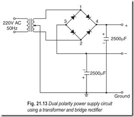
(7) Dual-polarity Power Supply Circuit Using A Transformer and Bridge Rectifier: In receivers where the power amplifier is operated from a dual voltage supply, a circuit such as that shown in Fig. 21.13 is used. In this configuration there is a centre-tapped transformer secondary and a standard bridge rectifier stack. The bridge functions as two independent half wave circuits rather than as a full-wave bridge. The centre tap on the power transformer secondary establishes the common ground for the system. Each half of the dual-voltage supply has its own filtering network. The values of the filter capacitors tend to fall in the 2,000 to 12,000 µF range.
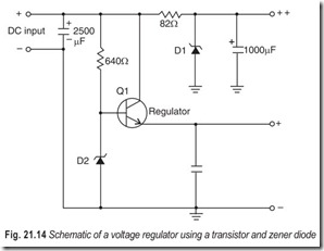
(8) Schematic of A Voltage Regulator Using A Transistor and Zener Diode: The power amplifier must depend upon reserve current capacity to furnish dc regulation. In some of the lower-level stages, however, a tighter degree of regulation can be afforded by relatively low-cost electronic regular circuits.
This tighter regulation is especially desirable on the power line to the f.m. tuner because variation in this dc level can deteriorate the stability of the entire f.m. section.
The power supply circuit in Fig. 21.14 shows two basic voltage regulator circuits used in present stereo equipment. One type is the simple zener iode-resistor regulator consisting of D1 and the
82 Ω current-limiting resistor. The zener diode has the ability to maintain a relatively constant voltage drop in the reverse direction in the face of rather severe excursions of the input level.The other dc regulator employs the current amplification factor of a power transistor to increase the regulating ability of the supply. This is the type of circuit generally used to supply power to the FM tuner while the circuit featuring only a zener diode can be used to feed those stages where the degree of regulation is not so critical. The base of the transistor is held at a constant voltage by zener diode D2 . If an increase or decrease in the output load forces the emitter voltage up or down, the resulting change in the base-to-emitter bias causes the collector current of the transistor to readjust, which maintains the output voltage at a constant level. A post-regulator filter capacitor minimises the abruptness of these changes and aids in further attenuation of the ripple component.
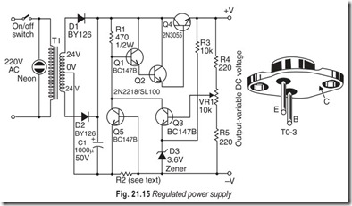
(9) Regulated Power Supply: No test bench is complete without a regulated power supply. Fig. 21.15 illustrates an interesting and useful circuit which gives 0.3% line regulation and 0.2% load regulation; output voltage can vary continuously from 4.6 V to 30 V and is capable of providing upto 3 amperes of current. It has a, short-circuit protection as well as current capability from 16 mA to 1 ampere.
Transformer T1 in the circuit provides full-wave 24 V ac diodes D1 and D2 rectify the voltage. Afterfiltration by C1 it will supply nearly 30 V dc. The main principle of the regulator is that when Q3
conducts more, Q4 conducts less-causing the output voltage to decrease. When the load sinks higher current, theoutput voltage decreases and thus a lower voltage is fed to the base of Q3 , R1
provides sufficient current to Q4 , through series pass Darlington pair comprising Q1 and Q2 , to increase the output voltage to the extent that it comes back to its original level. Hence the regulation is achieved.
By varying VR1 the output voltage can be changed from 4 V to 30 V. Variation in line voltage tends to change the output voltage but again the input voltage is restored as before and regulation is achieved.Transistor Q5 and resistor R2 constitute the short-circuit and overload protection circuit. Current limiting transistor Q5 starts conducting beyond a set load current determined by R2 . Once VBE
drop of this transistor exceeds 0.6 volts, Q5 conducts and current flowing to Q1 and Q4 gets grounded. Hence, the output voltage and current decrease to very low levels.Likewise, when output terminals are shorted, more than 0.6 volts develop across R2 reduced to a voltage and current that does not affect the load.
and output gets As Q4 is a power transistor (2N 3055) which draws very large current, it must be mounted on a proper heat sink.
To vary output current limiting point from 60 mA to 1 ampere, we must alter R2 from 10 Ω to 0.5 Ω respectively; 2.2 Ω resistor is sufficient for 300 mA load.
A limitation of this circuit is that we cannot achieve voltages less than 4.6 V dc, as we may not get lower voltage zener with good temperature coefficient values.
POWER SUPPLY CIRCUITS FOR STEREO AMPLIFIERS
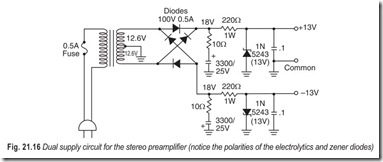
(1) Dual Supply: Fig. 21.16 is a schematic diagram for a simple split supply. The use of 1 Ω resistors on the filters keeps charging surges at a tolerable level to minimise the ripple content on the output.
Since each of the 220 Ω series resistors has to drop about 6 volts, it establishes a zener current of about 25 mA. The load current and zener current are additive through each source resistor, bringing each resistor’s dissipation close to one-half watt. To be conservative, 1 watt resistors should be used.
The transformer’s secondary voltage is not critical. Other standard values are usable, but if higher secondary voltages are used, the series resistor should be changed to ease the power dissipation requirements of the zeners.
The measurable hum level is a hundred millivolts and so will be undetectable in the amplified signal from the preamplifiers. High quality preamplifiers are virtually insensitive to hum levels even up to a millivolt or so.
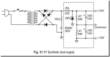
(2)Synthetic Dual Supply: A voltage divider can be used across a single dc supply line of 30 to 36 volts. If you have a 28 volt zener on hand, you can use a pair of resistors as dividers and stabilise the full voltage with the single zener, as shown in Fig. 21.17. It is extremely important to remember not to ground the output common line to any wire or chassis that will be routed to the power supply ground link through any direct connection. The output “common” line is 13 volts above ground with respect to the power supply
The series resistor is shown for a dc supply of 36 volt. The value may be changed according to voltage available by using the formula:
where Vz is the zener voltage, Ip is the total current requirement of the preamplifier, and Iz is the bias current through the zener.
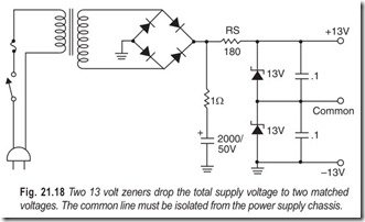
(3) A Split Supply: Fig 21.18 shows a method for effecting a dual supply using a pair of zeners as the voltage-divider pair. Again, the series resistor will depend on the rectified output voltage. In this case, the value can be calculated by :
In any event, the supply cannot be allowed to deliver more than a maximum of 30 V (15 V per leg) total to the preamplifier, so close tolerance zeners should be used for either supply configuration.
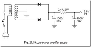
(4) Low Power Amplifier Supply: The 14 volt dc supply shown in Fig. 21.19 will provide sufficient power to operate a 10 watt stereo mini-amplifier. If you plan to build a complete stereo system, including the amplifier, you might want to build two of these supplies on a single chassis, and use one supply for each amplifier of the stereo pair.
The concept would give you two 13.8 volt outputs that you could regulate and use in reverse polarities for the preamplifier. The filter requirements are not especially critical because of the high level of audio accepted by the power amplifier. However, it is always good to use as much filtering as possible with audio circuits.
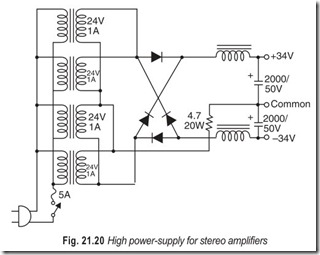
(5) High Power Supply: High power amplifiers require supplies capable of sustaining current drains of several amperes. The power supply for a 180 watt unit (actually 60 watts r.m.s. per channel) must be capable of delivering at least 2.5 amperes per channel under maximum load conditions (Fig. 21.20)
Some deviation in the output voltage, because of variations in the power line voltage or changing load conditions, is permissible. Both audio amplifier circuits have built-in compensation for limited fluctuations. Nonetheless, the output of the power supply should always stay within 10% of its created output, regardless of the line or load variations.
The most effective way to assure a relatively constant output under varying loads is to steer clear of capacitor input designs. An inductive termination (choke-input) at the rectifier results in a lower dc supply voltage, in general, but it assures optimum performance in terms of voltage stability.
HOW TO PROTECT YOUR EQUIPMENT FROM SPIKES, SURGES, AND BLACKOUTS
Your electrical power is just plain unreliable. Utility companies simply cannot provide the clean, consistent power required by sensitive computers and other electronic devices. An IBM study showed that a typical system experiences more than 120 power problems per month! Some problems are imperceptible, others are catastrophic. They include:
(1) Brownouts—temporary voltage dips that can cause system failures and data loss,
(2) Blackouts—complete losses of power that can cause unsaved data to be lost,
(3) Surges—short-lived voltage increases that stress electrical circuits and cause premature failure.
(4) Spikes—massive voltage increases that are capable of destroying your entire system
(5) Noise—electromagnetic interference [EMI] and radio frequency interference (RFI) that can cause intermittent errors in programs and data files. Three levels of protection are available:
(1) A surge suppressor protects your hardware by acting as a high-tech fuse to stop a spike before it reaches your computer.
(2) A line conditioner protects hardware and data against brownouts and surges only. It also filters out EMI and RFI by constantly correcting power transients.
(3) An uninterruptible power supply [UPS] protects both your hardware and your data. It contains an emergency battery that provides instant power if you experience a blackout, giving you time to save your work. A UPS also eliminates surges and spikes, and maintains even power during brownouts.
Buying power protection is a lot like buying insurance. You don’t appreciate it until you really need it.
UNINTERRUPTED POWER SUPPLY SYSTEMS (UPS)
Power failures, load sheddings, and low voltage have become our constant compansion. Over the years, the situation has worsened instead of improving. The business and work schedules get affected, students lose precious study time, and the family’s entertainment time disappears, not to mention the inconvenience caused during the winter. The problem is compounded with the popularity of PCs in the modern households.
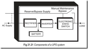
Commercial power supply is not capable of providing clean and consistent electric power demanded by sensitive equipment. Sensitive equipment requires a consistent supply of power of the correct specifications for their operation, hardware protection, continiuity of process, storage and transfer of information, and safety of Personal Computer network communication links, electronic medical equipment, industrial process control, remote installations like offshore operations, online applications such as airline reservations etc., are examples of such critical loads. Beyond any dispute, the installation of an uninterrupted power supply (UPS) system is nowadays accepted as being a vital element in the protection of sensitive equipment. The components of a UPS system are illustrated in Fig 21.21.
Types of UPS
UPS systems can be online, offline or hybrid.
Online UPS systems function even under normal supply conditions. The mains supply drives the rectifier/ battery charger. DC power is applied to the inverter and to the backup battery (for float charge). When the mains supply fails, the inverter draws power from the backup battery. The inverter provides a highly stable, low distortion A supply to the cirtical loads in a network environment where file-server is supporting many users and the task is mission-cirtical, online UPS is used. This system gives better performance but it is costly. Offline UPS systemsstart functioning only in the event of power failure. Under normal power conditions, the load is driven directly by the mains. When the supply fails or varies from the nominal value, the inverter provides A supply to the load. Automatic voltage regulation is not done, therefore, the output voltage does not remain constant. As compared to online UPS systems offline UPS systems are economical.
Hybrid UPS systems are basically offline units. The inverter is in parallel with the mains all the time, supplying power to the load continuously. The battery is not floated across the rectifier but charged from a small battery charger. When the supply fails, the battery is connected to the input of the inverter.
Battery-Life of the UPS System
The most critical part of the UPS sytem is the battery. The battery often represents half the original cost of a UPS system. It is the weakest link in the UPS system. An incorrect selection of the battery type may reduce the initial cost but would adversely affect the overall life of the system.
The battery life is determined by the UPS service conditions. For online UPS systems, the battery remains on floating charge for a longer time. Float performance characteristic has a strong influence on battery life.
Prolonged breakdowns can cause the battery to deep discharge several times in a week if not in a day. This in turn affects battery life drastically. As a thumb rule, a deep discharge below 80 per cent battery capacity reduces the life of the battery by 25 per cent.
Engine-Generator Back Up
There are certain areas of application of UPS where it may be necessary to maintain the power supply longer than the capacity of the battery of the UPS system. There are many situations where there are other essential loads in addition to the critical loads which require a supply without much interruption. These loads include emergency lights, cooling systems of critical loads, protection against fire, etc. Apart from these, there are other loads which are not that essential and can tolerate longer outage of power.
Computers and other critical loads cannot run for more than 15–20 minutes without cooling. Normally the cooling systems of critical loads such as airconditioners are not supplied through the UPS systems. This results in the shut-down of the critical loads such as airconditioners when the room temperature exceeds the allowable limits. Therefore, even if there is power to critical loads for a longer priod, these have to be shut- down because of over-temperature.
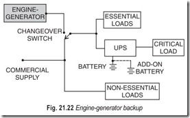
This problem can be overcome by incorporating an engine-generator as shown in Fig 21.22. This arrangement provides power to essential loads. The engine-generator is a stand-by power source which can be brought into service when the commercial power supply fails and the outage period remains more than 15 minutes. This is done by a changeover switch. The engine-generator can supply power to the critical and essential loads only and not all loads.
Normally, the commercial supply provides power to all loads, and the changeover switch is connected to the utility supply. The engine-generator is at rest. When the power fails, no power is available both to the non-essential and essential loads initially. Only the critical loads are supplied by the UPS. A period of 5–15 minutes is set for the UPS to run on the battery. After the expiry of the set period, the engine-generator starts automatically. When the generator stabilises and is ready to supply power, the changeover switch connects the generator supply to the UPS and essential loads. The UPS operates normally and the drainage from the battery ceases.
A UPS backed up by an engine-generator is one of the best solutions to provide cost- effective power protection for long durations. Care must be taken in selecting the engine- generator of a suitable rating for the given installation. The capacity of the generator must be sufficient to withstand the effect of sudden change of load, such as the starting of a compressor motor of the cooling systems which may cause a sudden shift of frequency. The change of frequency may, at times, exceed the limit permitted by the critical loads. However,
the UPS minimises this effect to a large extent and maintains the frequency and its rate of change within the tolerable limits.
EXERCISES
Descriptive Questions
1. Compare different types of rectifier circuits. Which of these rectifier circuits is preferred and why?
2. What are the relative merits and demerits of different types of smoothing circuits?
3. Discuss the need for voltage regulation. How is it achieved?
4. Explain the difference between a shunt regulator and a series regulator.
5. Draw the circuit of a synthetic dual supply and explain its working.
6. What is the need for a UPS system?
7. Distiniguish between online and offline UPS systems.
8. Illustrate the components of a UPS system.
9. Describe in details, with the help of an illustration, engine generator backup.
Fill in the Blanks
1. The ripple output of a half-wave rectifier is more …………………………… to smooth as compared to that of a full- wave rectifier.
2. The ripple output of a full-wave rectifier is…………………………… to smooth as compared to that of a half-wave rectifier.
3. The use of a bridge rectifier circuit gives full wave rectification without a…………………………… winding.
4. Filtering requirements are more stringent where…………………………… signal levels are involved.
5. Resistance smoothing element is only used for current, constant…………………………… applications.
6. Circuits using choke-input filters should be designed to cause…………………………… to flow through the choke at all times.
7. To stabilise the operating voltage, a voltage…………………………… is used.
8. The lower the required per cent regulation the…………………………… the supply for transistor and integrated circuit applications.
9. At maximum load…………………………… and minimum input…………………………… there must still be sufficient current flowing through the zener diode to…………………………… it in the breakdown region.
10. Better performance can be obtained by connecting two or more…………………………… voltage zener diodes in series to obtain the required output voltage.
11. Commercial power supply is not capable of providing clean and…………………………… supply of power.
12. The installation of a UPS system is a vital element in the…………………………… of sensitive equipment.
13. Online UPS systems function even under…………………………… supply conditions.
14. Offline UPS systems start working only in the event of…………………………… .
15. Online UPS systems give better…………………………… but are…………………………… .
16. Offline UPS systems are…………………………… .
17. The…………………………… is the weakest link in the UPS system.
18. For online UPS systems, the battery remains on…………………………… .
19. A deep discharge below 80 per cent battery capacity reduces the life of the battery by…………………………… .
20. An extra battery increases the…………………………… period.
21. Computers and other critical loads cannot run for more than 15 to 20 minutes without…………………………… .
ANSWERS
Fill in the Blanks
|
1. difficult 4. low 7. regulator |
2. easier 5. load 8. better |
3. centre-tapped 6. current 9. current, voltage, hold |
|
10. low 13. normal 16. economical 19. 25% |
11. consistent 14. power failure 17. battery 20. backup |
12. protection 15. performance, costly 18. floating charge 21. cooling |
