LOW LEVEL AMPLIFIERS
In low level amplifiers it is assumed that the signal level is small such that the signal “swing” is only over a small region of the load line around the dc operating point. The ac characteristics of the transistor can be assumed to be constant as long as bias stabilisation is used. A low level amplifier can amplify a small signal of micro volts to a level high enough to feed the driver stage of a power amplifier. Only on rare occasions will a single stage be sufficient, two or three stages being more usual. General points for consideration in the design of an amplifier are circuit configuration, number of stages, bias stabilisation, interstage coupling, gain control, frequency response and first stage signal-to-noise ratio.
CIRCUIT CONFIGURATION
The common-emitter circuit is the most convenient arrangement for low-frequency amplifier circuits. Its high current gain makes possible the use of resistance–capacitance coupling. Although the input resistance is normally of the order of one to two thousand ohms, it can readily be increased by inserting an un-bypassed resistor in the emitter circuit. There will be a loss of signal across the emitter resistance, RE and since it is common to both input and output circuits, it will also introduce negative feedback, thus reducingthe stage gain. The input resistance can also be increased by including a resistor RB in series with the input to the base. Again there will be a loss of signal across RB . A third method of obtaining some control of input resistance is by the choice of the operating emitter current. Reducing the emitter current will increase the input resistance. Another important feature of the common emitter circuit is that it results in a phase reversal of the signal. This phase reversal facilitates the use of negative feedback.
The common-base circuit gives voltage gain only. The current gain is always less than unity and so resistance–capacitance coupling is not possible. In order to obtain a power gain with coupled common-base stages it is necessary to use a step-down transformer to match the high output resistance of one stage to the very low input resistance of the next stage. The main use of the common-base stage in low-frequency amplifiers is where a very low input resistance, of the order of ten or twenty ohms, is required.
The common-collector circuit, more often called the emitter-follower circuit, is useful to obtain a very high input resistance with a low output resistance. The high input resistance is obtained due to the fact that the load resistance is in series with the emitter. The current gain is high, approximately the same as for the common emitter, but the voltage gain cannot exceed unity.
NUMBER OF STAGES
It is necessary at the start of any amplifier design to estimate the number of stages required. The required overall gain can be deduced from the input available and the output required. With low level transistor amplifiers it is usually best to consider the stages as current amplifiers, and to evaluate the current gain requirements. In some applications it may be convenient to include a stage mainly for some manipulation other than signal amplification, such as impedance transformation or frequency response control. Also with
many amplifiers some negative feedback will be included and in this case the gain requirements of the amplifier without feedback must be greater, depending upon the amount of feedback.
INTERSTAGE COUPLING
The ac output signal from a common-emitter stage can be coupled to the input of the next stage either by means of a transformer or by a resistance–capacitance combination. Maximum power gain will be obtained with a transformer having a suitable primary-to-secondary step-down ratio to match the output resistance of the first stage to the input resistance of the second stage. The turns step-down ratio will be typically between five and ten-to-one. Transformers, however, are relatively expensive components and are also susceptible to magnetic pick-up. Accordingly they are rarely used in low level transistor amplifiers.
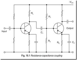
With resistance–capacitance coupling the input resistance of the second stage effectively becomes the load resistance of the first stage, and so the input resistance and the load resistance of the first stage are the same. Thus the voltage gain will equal the current gain and the power gain will equal the current gain squared. If the current gain is 50, the power gain will be 2500, i.e. 35 dB.
The effective ac load on the transistor consists of several components in parallel with the load resistance RL , the output resistance of the transistor, the base bias resistors R1 and R2 , and the input resistance of the next transistor. The only useful part of this load is the input resistance of the next transistor—the other components all represent loss, and when evaluating the overall gain of a transistor amplifier it is necessary to take these losses into account.
The value of the coupling capacitor depends upon the required low-frequency response of the amplifier. As the signal frequency is decreased, a point will be reached where the amplifier gain starts to decrease due to the increasing impedance of the coupling capacitor. The gain will have fallen by 30 per cent (3 dB) at the frequency at which the reactance of the coupling capacitor equals the total resistance in series with it. This series resistance is equal to the load resistance of the previous stage plus the input resistance of the next stage.
Referring to Fig. 19.1 : ![]() where RL = 2.5 kΩ, and Rin = 1.5 kΩ. For a 3 dB loss at 25 L in Hz, a coupling capacitor of 1.5 µF will be required.
where RL = 2.5 kΩ, and Rin = 1.5 kΩ. For a 3 dB loss at 25 L in Hz, a coupling capacitor of 1.5 µF will be required.
The value of the emitter resistance decoupling capacitor C2 also depends upon the required low frequency response. The gain of the amplifier will fall by 3 dB at the frequency at which the reactance of the capacitore C2 quals the emitter resistance RE shunted by the resistance presented by the transistor. This latter is approximately the output resistance of the transistor in the common-collector arrangement and equals.
(RG + rb ) (1 – α) …(19.1)
RG will be RL in parallel with R1 and R2 , and with the values assumed earlier RG = 1670 Ω, giving a transistor input resistance of approximately 40 Ω. The required capacitance for a 3 dB fall in gain at 25 Hz will be 150 µF.
GAIN CONTROL
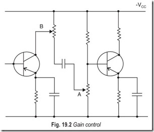
The gain of a transistor amplifier can be adjusted by making the coupling network between two stages a variable attenuator. The attenuator must be designed so that it has negligible effect on the frequency response of the network. The dc operating point of either of the transistors, Fig 19.2, shows two suitable methods of control.
That shown at A is probably the better and is most widely used. It has no effect on the bias setting and has only a slight effect on the low-frequency response. The control shown at B has no effect on the low- frequency response, but will alter the dc voltage across the first transistor.
FREQUENCY RESPONSE CONTROL
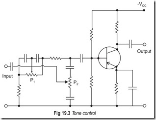
In audio amplifiers control of frequency response is usually referred to as “tone control” and is used to attenuate or accentuate the response at the low or high frequency end of the frequency band.The control can be carried out by incorporating frequency dependent circuits in the coupling network between two stages. Increasing the effective capacitance in parallel with the load resistance of a transistor will reduce the high-frequency response, and by varying the effective capacitance in the coupling circuit the low-frequency response can be controlled. A typical arrangement is shown in Fig. 19.3. Potentiometer P1 controls the low-frequency response and P2 controls the high-frequency response.
NEGATIVE FEEDBACK
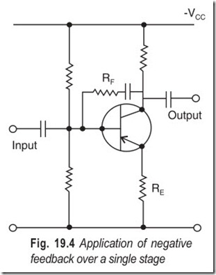
The gain of an amplifier can be stabilised and the internally generated distortion reduced by introducing negative feedback. This can be applied from the output to input of a single stage or alternatively over several stages. With single stage common-emitter amplifiers, negative feedback can be obtained in two ways; by feedback from collector to base (Fig. 19.4) via RF , or by including an unbypassed resistor RE circuit. The latter is very useful and is commonly used.
Such a resistor increases the input resistance to the transistor. This reduces distortion caused by the nonlinear characteristic of the base-emitter diode. At the same time some loss of gain results.
In multistage amplifiers the feedback may be introduced in series with the source signal (series or current feedback) or in parallel with the input signal (shunt or voltage feedback). Series feedback is illustratedin Fig. 19.5 (a), the signal developed across resistor RE in the emitter of the second transistor being fed back to the base of the first transistor. Shunt feedback is shown in Fig. 19.5 (b), the signal appearing at the collector of the second transistor being fed back to the emitter of the first transistor.
LOW NOISE CONSIDERATIONS
The noise figure, NF, of an amplifier is defined by the equation:
An ideal amplifier should amplify the incoming signal and noise without changing the signal-to-noise ratio, that is, the noise figure would be unity (i.e. 0 dB). In practice, some extra noise is generated in the transistor and so the noise figure of a transistor amplifier is always greater than unity. The nearer the noise figure is to unity, the better is the amplifier.
If an amplifier is required to amplify signals with amplitudes of the order of microvolts, special attention must be paid to the design from the low noise aspect. The noise figure of a transistor amplifier is dependent upon the value of emitter current and the source resistance. As the emitter current is reduced the noise figure falls, but eventually it starts to rise again as the current gain decreases at very low currents. In general, the emitter current for best low noise operation will be between 10 µA and 200 µA. For germanium transistors it will be towards the top of this range, and with silicon transistors towards the lower values. For a given value of emitter current there will be a certain value of resistance for minimum noise figure. As the emitter current is decreased, the optimum value of source resistance increases. In deciding upon the value of emitter current for a particular application, other considerations such as level of leakage current and stability against temperature must be taken into account, and so a compromise must be necessary.
REQUIREMENTS FOR AUDIO PREAMPLIFIERS
For the listener the most common source of program is undoubtedly the radio, followed by disc and tape in that order. The microphone is normally used only in connection with a tape recorder, apart from public address applications.
Radio tuners specially designed to feed a low-level audio signal to high quality amplifiers are now becoming popular. Tuner outputs vary, but it is normal to expect a signal level between 150 mV and 250 mV. Provision for an input to accept a tuner signal is, therefore, desirable and this input should have a high impedance normally from 100 kΩ to 500 kΩ.
Crystal pick-ups working directly into a preamplifier require a high input impedance, otherwise there will be considerable loss of bass. Since, they may produce as much as 1 V output, provision to handle this signal has to be made at the preamplifier input, and extra precautions must be taken to prevent damage to the input transistor if the pick-up cartridge is dropped on the record, when a voltage of the order of 100 V may be generated. An input impedance of 0.5 to 1 MΩ would be considered normal for crystal pick-up inputs and a preamplifier would be designed to accept a signal level of about 250 mV.
Magnetic pick-ups, very suitable for high fidelity applications, have a lower voltage output than crystal pick-ups and consequently a high gain amplifier including frequency correction is essential. Assuming that the preamplifier unit must deliver 300 mV to fully drive the power output stages, a gain of around 100 would be required, since an output voltage of only 3 mV could be expected from the pick-up. This leads to complications in the design of the amplifier and precautions have to be taken to prevent feedback and instability. Care must be taken to avoid hum pick-up, and earth loops should be kept as small as possible. An input impedance of around 50 kΩ is required for a magnetic pick-up.
For the reproduction disc recordings the preamplifiers circuit should provide facilities for equalisation of the recording characteristic. Practically all present day domestic disc recordings are in accordance with the R.I.A.A. characteristic but to enable older recordings to be played, a switch providing a choice of equalisation characteristics is sometimes used.
In addition to disc records, facilities for tape replay are often required. Tape recorded outputs are of two kinds: a high-level pre-recorded output of the order of 250 mV, or a low-level output direct from a playback head. The low-level output may be of the order of 300 µV and will depend, amongst other things, on the tape speed. An input impedance of the order of 10 kΩ would be normal for an input direct from a magnetic head.
Microphone inputs are not very common unless public address applications arise. The crystal microphone works under similar conditions to the crystal pick-up, but it has a frequency response incomparable to the dynamic microphone which is favoured for high fidelity work. The dynamic microphone, like the magnetic pick-up, produces only a low signal voltage of the order of 3 or 4 mV, and requires an amplifier input impedance of between say, 20 kΩ and 50 kΩ.
To avoid interaction between the various signal inputs it is desirable that inputs not in use are shorted to earth. An input selector switch, which also performs the earthing function is, therefore a useful facility.
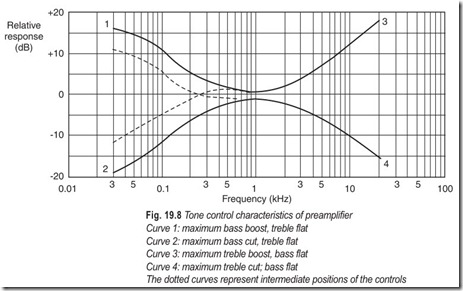
Other facilities which must be provided in addition to the input selector, are the volume and tone controls. From 10 dB to 20 dB boost and cut of both bass and treble is normally provided, but values much in excess of that are seldom required since the basic use of controls is to correct the reproduced sound image, not distort it further.
A reduction in volume causes a considerable drop in bass. At low volume levels, therefore, realistic sound reproduction requires bass boosting and to avoid the listener having to reset the bass control each time the volume is adjusted, a physiological volume control is sometimes used. This automatically increases the bass at low volume levels to make up for the insensitivity of the ear in that part of the spectrum. It is sometimes known as a contour control.
Artificially boosting the mid-range at a selected frequency between 2000 and 3000 Hz produces the effect of bringing the vocalist or musical instrument nearer to the listener, and is known as presence. It is also a valuable facility for correcting mid-range absorption in imperfect listening conditions. A presence control is sometimes fitted on amplifiers and gives a lift of around 6 dB at a selected frequency, normally between 2,000 and 3,000 Hz.
Some stereo installations have a sound source width (or dimension) control. This is a continuously variable control which at one end of its travel provides 100% in-phase cross-talk between channels and results in mono. The sound source then appears mid-way between the speakers, provided both speakers are in-phase and assuming accurate balancing. When the control is turned in the opposite direction anti- phase cross-talk up to about 20% can be introduced, the two channels becoming further and further separated as the control is advanced. At about 24% cross-talk the sound picture breaks up and becomes unpleasant. The apparent width of the “sound stage” can thus be varied with this control.
Finally, a number of filters may be employed. Rumble and scratch filters can be used to make up for the deficiencies of turntables and discs respectively, the incorporation of a scratch filter having the additional advantage that it may be used to remove the noise from radio tuner signals.
For greater refinement low-pass and high-pass filters maybe incorporated in the reproduction chain. The variable cross-over filters normally provide a selection of frequencies at which roll-off commences and a fixed rate of attenuation is maintained: the variable slope filters, on the other hand, start to roll off at fixed frequencies and the rate of attenuation can be varied in steps.
A signal-to-noise ratio of 70 dB would be acceptable to a critical listener in a very quiet room. Modern transistors, and especially carbon film resistors, used in low level circuits, make possible the achievement of signal-to-noise ratios even better than this.
Distortion in all its forms should be as low as possible. It has been suggested that harmonic distortion below 1% is undetectable by the ear, but with modern semiconductors entailing transformerless configurations it is fairly easy to arrange for the harmonic distortion to be only 0.1%. What is probably more important is the level of intermodulation products arising from non-linearity. A very small percentage of intermodulation products can be easily detected by the ear and this objectionable form of distortion occurs mainly in the output stage.
It is particularly important that distortion arising in the input stages is kept very low. Further amplification will soon raise the level of any distortion beyond an acceptable limit. High-gain low-noise transistors may be used in output stages, with heavy negative feedback to obtain linear operation conditions.
LOW LEVEL AMPLIFIER CIRCUITS
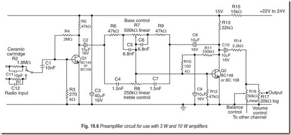
(1) Preamplifier For use With the 3 W and 10 W Amplifiers The circuit for a two stage preamplifier which may be used with the 3 W and 10 W amplifiers, is illustrated in Fig. 19.6. The first stage uses a low- noise BC 149 or BC 109 transistor and the second stage a BC 148 or BC 108 transistor.The input stage provides matching for a ceramic cartridge and for radio, the resistor R1 being chosen to give the required sensitivity in the latter case. A capacitor C 12 is connected in parallel with R1 , the value of the capacitance being chosen to give with R1 a time constant of 18 µs. The second stage provides comprehensive tone control, with 10 dB boost and cut at 100 Hz and 10 kHz. This stage is followed by a simple balance control for stereo use and a volume control.
Performance:
|
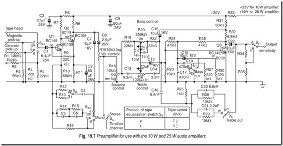
(2) Preamplifier for use with the 10 W and 25 W Audio Amplifiers A preamplifier for use with the 10 W and 25 W audio amplifiers is shown in Fig. 19.7.
Transistors Q1 and Q1 form a directly coupled pair, the base voltage of Q1 being derived from the emitter of Q2 . Equalisation for tape head, magnetic pick-up, ceramic pick-up and radio inputs is obtained by feedbackfrom the collector of Q2to the emitter of Q1 .No value is given for R , the input resistor for radio position, because this must be chosen to suit theavailable signal. The sensitivity at the base of Q1 is 7.5 mV for 200 mV output.
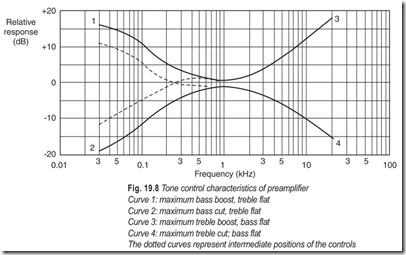
Transistor Q3 is used in a feedback control circuit which gives a voltage gain of three times. A circuit with linear potentiometers has been used because more boost can be obtained, and also because of the difficulty in obtaining and matching reverse-logarithmic potentiometers. A BC 149 or BC 109 is used because a low-noise device is required in the first stage after the volume control. The tone control characteristics are shown in Fig. 19.8.
The working point of Q3 is fixed by R 23, R 24 and R 26, ac feedback being removed by decoupling capacitors, C 17, C 18 or C 19. By switching these capacitors, bass cut is obtained. Networks can also be switched in by SE to give treble cut.Resistors R 34, R 35 and switch Sf are required in the preamplifier for use with the 25 W amplifier only.
When a high sensitivity speaker is used with the 25 W circuit, in quiet listening conditions, the noise originatingin Q3is perceptible even when a low noise transistor is used. Since the full sensitivity will not be required under these conditions, a switched attenuator is used at the output of the preamplifier, reducing the sensitivity and noise by 12 dB.
Performance :
Sensitivity at 1 kHz for 200 mV (25 W version) or 400 mV (10 W version) output:
|
Ceramic pick-up |
170 mV |
|
|
Magnetic pick-up |
4 mV |
|
|
Tape head with tape |
ed of 7 1/2 ips |
6.5 mV |
Total distortion for 200 mV output with <0.02%
volume control at maximum
UNIVERSAL PREAMPLIFIER
This Universal preamplifier is suitable, for use with a wide range of power amplifiers since it will deliver a nominal output voltage of 440 mV/1kΩ.
The preamplifier employs highlevels of ac and dc feedback ensuring a very low distortion level (<0.15%) and variations from the nominal performance characteristics given here due to component tolerances are negligible.
There are five different inputs: crystal pick-up, magnetic pick-up, radio tuner, tape recorder and magnetic microphone. In the magnetic pick-up position the amplitude/frequency characteristic is in accordance with the R.I.A.A. standard. In addition the preamplifier provides an output signal of 0.35 mV/1 kW for tape recording.
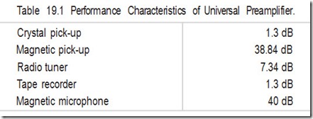
In Table 19.1 the input sensitivity, input impedance, frequency response (–1dB points) and the unweighted signal/noise ratio are given for the various types of inputs. Sensitivities and input impedances are given at a frequency of 1,000 Hz, for an output signal level of 440 mV. The signal/noise ratios are given for an output signal level of 20 dB below 440 mV, i.e., 44 mV.
The block diagram of the universal preamplifier is shown in Fig. 19.9. Four npn transistors of the BC 147 family are employed. The first two amplifier stages are directly coupled with dc feedback, and different amounts of ac feedback are applied depending on the type of input.
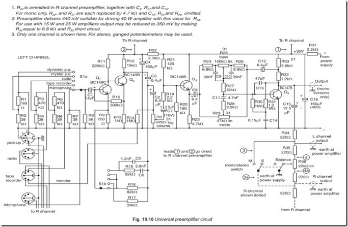
The circuit diagram of the universal preamplifier is shown in Fig. 19.10. In the magnetic pick-up position the feedback loop R15 – C5 – C6 provides equalisation according to the R.I.A.A. characteristic. All other inputs are frequency independent and have a flat response. To obtain a low noise level BC 144/149 C has been used as the input transistor, whilst the second preamplifier is a BC 149 B. The overdrive ratio of the first two stages is 20 dB with respect to 350 mV across volume control R 18. The voltage gains from the inputs to the top of the volume control at 1,000 Hz are given in Table 19.1
The tone control circuit is of the feedback type, the bass and treble potentiometers being connected in the feedback loop between the collector and base of the output transistor Q4 . This feedback system has the advantage of a low output impedance being maintained, while the bass and treble controls can be varied independently over a wide range. When the sliders of the bass and treble control potentiometers are at mid- positions, the feedback is practically independent of frequency.This preamplifier may be used in mono applications and for such purposes the audio output is taken from the collector of the output transistor Q4 . This stage has a voltage gain of the order of 2.6 dB. If the input circuit of the power amplifier has no series capacitor then an electrolytic capacitor of 6.4 µF/25 V should be inserted between the preamplifier and the power amplifier.
For stereo applications two preamplifiers are used, the collectors of the output transistors being joinedby a series network comprising C15 –34– 35– 36 and so on in the other channel. R36 serves as the stereobalance control, its slider being connected to earth when stereo program material is reproduced. At themidpoint of its setting the decrease in voltage amplification is about 0.6 dB. Resistors R34 and R35 are mountedon the printed-wiring board and the leads marked 3 and 4 in Fig. 19.10 are taken to the externally mountedmono/stereo switch and balance control respectively. Audio output is taken from the junction of R34 and R35 any power amplifier without an input capacitor is used, a 6.4 µF/25 V electrolytic capacitor must beinserted in series, its negative connection to the junction of R34 and R35 .
In the mono position of the mono-stereo switch, the output voltages of the two amplifiers are combined, the slider of the balance control being disconnected from earth.
With the component values shown in Fig. 19.10, the preamplifier will deliver a nominal output voltage of 440 mV. This is the correct level for driving the 40W power amplifier. The input signal level required for the 15 W amplifier is, however, 350 mV and the preamplifier output voltage can be reduced to this level bymaking R33 equal to 6.8 kΩ and replacing R32 by a shorting link. Other values of output voltage may beobtained by changing the values of R32 and R33 correspondingly.
The overdrive ratio of the complete pre-amplifier is 20 dB with respect to the nominal output voltage of 440 mV, so the undistorted maximum output is > 4.4 V.
Power Supply Connections: The supply voltage for the preamplifier is 30 V. In view of the number of ways in which the preamplifier can be used, the circuit changes are given separately as follows:
(1) Regulated Supply: Where the output power amplifier has a regulated supply unit, the dc voltage for the preamplifier can be obtained from there via the series resistor R37 . Accomodation for this resistor and itsassociated capacitor has been provided on this printed-wiring board.
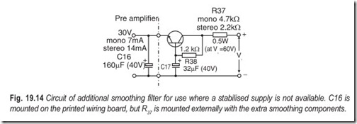
(2)Unstabilised Supply: If no stabilised supply is available, the use of an additional active smoothing filter is recommended and a circuit is shown in Fig. 19.14. This filter should be connected between the pre-amplifier and the power supply unit. Capacitor C16 remains on the printed wiring board, but R37 now has to be mounted externally with the smoothing circuit.
(3) Mono: For mono applications, where only one preamplifier is employed, resistors R11 and R37, are each replaced by 4.7 kΩ. Output circuit components C15, R34 and R35 are also omitted, since the audio output is taken from the collector of Q4.
(4) Earthing: The interconnection of units to avoid earth loops should be followed wherever possible, otherwise feedback troubles are likely to arise.
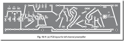
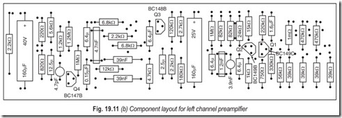
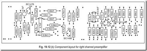
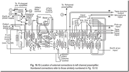
(5) Component Layout: The printed-wiring board for the L-channel preamplifier and its component layout are shown in Fig. 19.11, whilst those for the R-channel are shown in Fig. 19.12. The external connections which have to be made to the L-channel preamplifier are shown in Fig. 19.13. The volume, balance and tone controls, together with mono/stereo switch and input selector switch are mounted on the front panel of the unit enclosure. Input sockets would normally be situated on a rear panel. For stereo installations the L and R-channel printed-wiring boards should be mounted reasonably close together in order to keep interconnections as short as possible. Hafler’s Preamplifier is shown in Fig. 19.15.
EXERCISES
Descriptive Questions
1. What are the different circuit configurations and their specific fields of application?
2. How will you estimate the number of stages while designing a multistage amplifier?
3. Which method of interstage coupling is prefered in low level amplifiers and why?
4. How will you adjust the gain of an amplifier?
5. How will you adjust the frequency response of an amplifier?
6. Explain the significance of negative feedback.
7. What are the different methods of applying negative feedback?
8. How will you ensure that the noise figure in an amplifier is nearer to unity?
9. Briefly explain the requirements for audio preamplifiers. How are these requirements met?
Fill in the Blanks
1. In low level amplifiers the signal level is …………………………………………………..
2. A low level amplifier accepts a small signal and amplifies it to a level ………………………………………………….. enough to feed the ………………………………………………….. stage of a power amplifier.
3. The common emitter circuit is the most ………………………………………………….. arrangement for ………………………………………………….. frequency amplifier circuits.
4. Phase reversal facilitates the use of ………………………………………………….. feedback.
5. The common base circuit gives ………………………………………………….. gain only.
6. The main use of the common base stage in low frequency amplifiers where a very low ………………………………………………….. resistance is required.
7. The common collector circuit is useful to obtain a………………………………………………….. input resistance with a ………………………………………………….. output resistance.
8. With low level transistor amplifiers it is usually best to consider the stages as ………………………………………………….. amplifiers.
9. Transformers are relatively expensive components and are also susceptible to………………………………………………….. pick-up.
10. The value of the coupling capacitor depends on the required…………………………………………………..frequency response of the amplfier.
11. The gain of a transistor amplifier can be adjusted by making the………………………………………………….. network between two stages of………………………………………………….. attenuator.
12. In audio amplifiers control of frequency response is usually referred to as ………………………………………………….. control.
13. The tone control is used to ………………………………………………….. or ………………………………………………….. the response at the lower high frequency end of the frequency band.
14. The gain of an amplifier can be ………………………………………………….. and the internally generated distortion reduced by introducing ………………………………………………….. feedback.
15. In an ideal amplifier the noise figure would be ……………………………………………………
16. To avoid interaction between various signal inputs it is desirable that inputs not in …………………………………………………..are shorted to……………………………………………………
17. Harmonic distortion below …………………………………………………..is undetectable by the ear.
18. High-gain low-noise transistors may be used in output stages with heavy…………………………………………………..feedback to obtain ………………………………………………….. operating conditions.
ANSWERS
Fill in the Blanks
|
1. small 4. negative |
2. high, driver 5. voltage |
3. convenient, low 6. input |
|
7. high, low |
8. current |
9. magnetic |
|
10. low |
11. coupling, variable |
12. tone |
|
13. attenuate, accentuate |
14. stabilised, negative |
15. unity (0 dB) |
|
16. use, earth |
17. 1% |
18. negative, linear |
