INTEGRATED AMPLIFIERS
Integrated circuits in the audio offer a number of special advantages. Not only where small size is the main consideration but also on grounds of cost, the use of integrated circuits is a particularly attractive alternative to discrete components.
The main advantage of employing integrated circuits lies in the use of less discrete components which require individual storage, handling and mounting.
The reduced dimensions of an integrated circuit make it of special appeal for microphone applications. With capacitor microphones, for example, the preamplifier may be mounted in the body of the microphone close to the sensitive element. Another clear example is that of the hearing aid amplifier which, by employing an integrated circuit, can be completely inserted in the ear.
OPERATIONAL AMPLIFIER
Linear integrated circuits are found in four main areas :
● Power amplifiers (audio applications with 1 watt or more of output power).
● High frequency amplifiers (r.f., video and wide band-dc to 75 MHz).
● Differential operational amplifiers (high input resistance and open-loop gain).
● Voltage regulators (for example, up to 0.6 A at 40 V, low output impedance of 20 mΩ)
The differential operational amplifier is the difference or differential amplifier, which is particularly suited to integrated circuit technology.
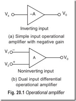
We will consider the IC here mainly as a “black-box” device, only occasionally referring to its schematic structure. However, basically, a small monolithic integrated circuit consists of a single chip of silicon, typically 40 by 40 mils in area, in which bothactive and passive components have been diffused and then interconnected. Hybrid circuits also exist that are a mixture of diffused and thin film devices. ICs may be packaged in circular metal “cans” with upto 12 leads, in plastic “in-line” packages with upto 16 leads, or in flat packages with over 32 leads. Originally used to perform the mathematical functions such as addition, sign changing, integration, differentiation etc, in analog computers, the operational amplifier is now found in many other applications, notably in control systems. Basically, it consists of a very high gain dc (direct coupled) amplifier with high input impedance and low output impedance. The early operational amplifiers had only one input, and the output was always inverted with respect to the input. However, general purpose operational amplifiers now available are usually of the differential type, where both inverting and noninverting inputs are available.
It is understood that all voltages are with respect to ground, so the ground line is not usually shown. In Fig. 20.1 (a), V0= AVs; in Fig 20.1 (b), V0 = AV2 = A(V2 –V1 ), where V2 and V1 are measured with respect to ground.
Thus, A is the differential voltage gain, Ad , since it amplifies the difference in input voltages. Of course, if either V1 or V2 is at ground level, as in many operational applications, Vo = AV2 or –AV1 respectively.
The amplifier’s gain, A, is also referred to as the open loop dc gain and may be anywhere from 60 dB (1,000) to 140 dB (10 million), so they are used in circuits with considerable negative feedback.
An operational amplifier is a gain block with an infinite input impedance, an infinite open-loop (no feedback) gain, and a zero output impedance. In reality, these paper specifications are never realised. Available IC op-amps have an input impedance of a megaohm or more, an open-loop gain of over 100,000 (approaching 1,000,000 in some), and an output impedance of less than 100 Ω.
The key to the operation of an op-amp is the feedback loop. This is shown in Fig. 20.2. An impedance is connected between the inverting or minus input and ground. The ratio of the feedback impedance to the ground impedance determines the closed-loop gain of the stage. To realise a gain of 10 (20 dB), the value of the feedback resistor must be ten times greater than the ground resistor. If a gain of 1000 (60 dB) is needed the feedback resistor value must be 1000 times greater than the ground resistor.
Since this can lead to either a low input impedance or instability (depending upon the op-amp), designers often use other tricks to raise both the gain and the input impedance. One such trick is to connect the input resistor to the negative input in series with the signal path. A typical value for this resistor might be on the order of 10 kΩ. A 1 MΩ feedback resistor is returned to a voltage divider across the output. The value of the ground resistor from the positive input must be equal to the feedback resistor rather than the other input resistor; otherwise, capacitor coupling is needed. The only disadvantage with an op-amp is that it must be operated from either a dual voltage supply or from a single-ended supply with dropping resistors and zener diodes arranged to simulate a dual voltage supply.
THE TAA 300 INTEGRATED CIRCUIT
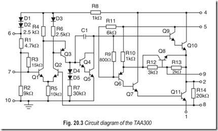
The circuit diagram of the TAA 300 is shown in Fig. 20.3. The TAA 300 consists of an input stage (Q1 and Q2), a driver stage (Q3 to Q5) and an output stage (Q6 to Q11). The input stage is a differential
amplifier. Since resistor R5 in the common emitters of the differential stage is very large with respect to the differential resistance of the transistors, it can be regarded as a constant current source.
The voltage at the base of Q1 is obtained by means of a low resistance voltage divider across the supply. Resistor R3 between the voltage divider and the base of Q1 increases the input impedance to about 15 kΩ. Two diodes are connected in series with R1 so that the voltage at the base of Q1 does not vary directly with the supply voltage. This allows the circuit to be used at supply voltages of 4.5 to 10 V. The point below the two diodes in the bias network of the first transistor is connected to pin6, thus enabling the supply line to be decoupled by means of an external capacitor. The layout of resistors R1, R2 and R8 is such that the spread of the base voltage of Q1 remains below 5%.
The driver stage consists of two npn transistors Q4 and Q5 in cascade. The dc coupling between the differential input stage and the driver stage is by means of a pnp transistor (Q3). This transistor has the function of level shifter, but it also presents a symmetrical load to the differential input stage. Consequently the noise factor of the input stage is no worse than that of a single transistor, whereas the advantages of a differential input stage are maintained.
The voltage gain of the driver stage is rather high and therefore this stage is used to cut off the frequencies above the audio spectrum by means of a small integrated capacitor C1 inserted between the base of Q4 and its collector. The voltage gain of the cascade driver stage will be about 200 when the quiescent current of the stage is 0.47 mA. This gain figure, in combination with a collector-base capacitance C1 of 10 pF, makes the capacitance between the base of Q4 and earth about 200 × 10 = 2000 pF.
Without feedback the upper frequency is limited to approximately 3 kHz (–3 db), the total frequency response can be expanded to about 30 kHz (–3 db) by using large overall feedback. To reduce the spread of the input impedance of this stage, and thus the spread in cut-off frequency, a resistor of 30 kΩ is shunted across the input of the driver stage. D4 and D5 are connected in series with the resistor to decrease the current of the pnp level shift transistor (Q3) and to stabilise the collector current of Q4 and Q5 against temperature variations.
In the TAA 300, the conventional complementary pair principle is used. This gives a very simple and stable direct-coupled single-ended push-pull output stage.
To reduce the collector dc current of the driver transistor the output transistors must have large current gains, therefore two transistors in cascade are used. The output stage is made complementary by placing pnp transistor Q6 in front of the lower cascade. Symmetrical drive of the output transistors is ensured by making the current gain of the pnp transistor unity.
The output voltage is limited only by the knee voltage of the output transistors Q10 and Q11 and, for symmetrical clipping of the output signal, a mid-point voltage of half the supply voltage is required.
The quiescent current of the output stage could be stabilised against the influence of battery and temperature variations of the VBE’s of Q9, Q10 and Q6 by using three diodes. In the TAA300 these diodes are replaced by transistor Q8 and resistors R12 and R13. Since the integrated components may spread, it should be possible to adjust the quiescent current of the output transistors, for which purpose the base and emitter of Q8 have external connections.
For a supply voltage of 9 V, the total quiescent current consumption must be preset at 8 mA. The typical current consumption of all stages (except for the output stage) is then about 3.55 mA as shown:
|
– |
bias network of the input stage |
500 µA |
|
– |
total current of differential input stage |
380 µA |
|
– |
driver stage |
470 µA |
|
– |
typical collector current of stabilisation transistor Q8 |
2100 µA |
|
– |
collector current of Q7 and Q9 |
100 µA 3550 µA |
The typical quiescent current of the output stage is therefore (8 – 3.55) = 4.45 mA which is necessary to minimise the crossover distortion.
When this amplifier is used as a normal audio amplifier it is permissible to assume a maximum dissipation of 500 mW at a battery voltage of 9 V.
The thermal resistance of the TAA300 without heat-sink is 225°C/W. Due to the good thermal coupling between the output transistors and the stabilising components, use can be made of the high junction temperature permitted in silicon transistors. With a maximum dissipation of 500 mW and the maximum crystal temperature of 150°C, the 1 W amplifier can be used without heat-sink upto an ambient temperature of 150 – (0.5 × 225) = 37.5 °C.
Taking into account a maximum voltage of 10 V and continuous sine-wave drive, the maximum dissipation is 750 mW. For this condition the thermal resistance can be improved by means of a cooling clip.
The cut-off frequency (– 3 db) at the high frequency side is determined mainly by the integrated 10 pF capacitor between the collector and the base of the driver transistor Q4, together with the applied feedback. The –3 db point for the lower frequencies is determined by the external capacitors.
The distortion level at an output power of 0.5 W is less than 1%. Crossover distortion is very small and due to the stabilisation of the quiescent current, it remains small even when the supply voltage shifts from 5 to 10 V.
Typical noise input voltage is about 2 µV, measured over a bandwidth from 30 Hz to 10 kHz with a source impedance of 2 kΩ. Related to an input signal of 8.5 mV, this means that the signal-to-noise ratio is 73 db. With the input short circuited, the r.m.s. noise output voltage is 280 µV, which represents a noise power of 80 dB below the maximum output power of 1W.
The preferred output power can be obtained by choosing the appropriate speaker load. However, a speaker load below 8 W is not permissible because the peak collector current of the output transistor would be too high.
1W TRANSFORMERLESS CLASS-B AUDIO AMPLIFIER USING IC-TAA300
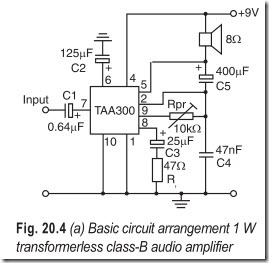
In many portable audio applications the required output power does not exceed 1W. The sensitivity and input impedance in this case should be such that the maximum output power is obtained when the input is connected to a ceramic pick-up element or a detector in a portable radio. Other requirements are that the circuit should still operate at half the nominal supply voltage and that the total current drain is low. Furthermore the complete audio circuit should be compact, easy to mount, have a low noise, and a reasonably low distortion factor. To meet these requirements the TAA300 has been specially developed. It contains a silicon chip of only 2 mm2, on which 9 planar npn transistors, 2 pnp transistors, 4 diodes, 14 resistors and 1 capacitor are integrated. The TAA 300 requires a few external components as shown in the basic circuit of Fig. 20.4 (a).
Performance Specifications (each channel)
Nominal power output 1W into 8 Ω load
Sensitivity (1000 Hz) for Po = 1W
pick-up (1000 pF) 1.5 V
at TAA 300 input 8.5 mV (typ)
Input impedance of TAA-300 10 kΩ (typ 15 kΩ)
Frequency response (–3 db) 120 to 26,000 Hz
Total harmonic distortion at Po = 1W 10%
At onset of clipping Po = 0.8 W 1%
Unweighted signal noise ratio (ref. Po = 1W) 73 db
Voltage feedback factor 10
Nominal supply voltage 9 V
Current consumption at Po = 1W 180 mA (typ)
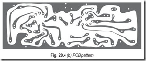
The p.c.b. layout for 1W amplifier is given in Fig. 20.4(b)
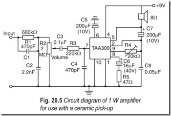
Figure 20.5 shows the practical circuit for use with a ceramic pick-up. The sensitivity for a source capacity of 1000 pF is 1.5 V for 1W output and the half power frequency response is 80 Hz to 26,000 Hz. The 0.05 µF capacitor must be directly connected across pins 1 and 2 and a ceramic type should be used. Similarly, the 470 pF capacitor should be directly connected across pins 7 and 10. Equalisation according to the RIAA characteristic is provided.
When using a practical low-cost power supply with an IC filter (5 Ω decoupling resistor) and an overall impedance of 16 Ω the rms output is 600 mW for 10% distortion (1% upto 500 mW). Under these conditions no heat-sink would be necessary for an ambient temperature upto 50°C.
THE TAA320 INTEGRATED CIRCUIT
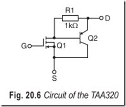
The TAA320 is a monolithic integrated circuitcomprising three components mounted in a T0–18 envelope: a MOS transistor of the p-channel enhancement type, an npn silicon transistor and a resistor. Its circuit is given in Fig. 20.6.
The biasing resistor R adjusts the operating current, Is, of the MOS transistor. Since its transconductance is proportional to Is, resistor R must be as small as possible to obtain maximum gain; on the other hand a low value reduces amplification of the silicon transistor. A value of about 1 kΩ gives optimum overall transconductance of the whole integrated circuit.
The TAA320 has advantages in that it combines a high transconductance with a high input impedance and low noise level.
PICKUP AMPLIFIER USING IC-TAA320
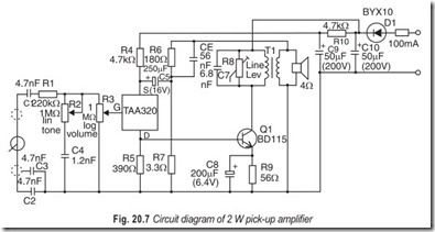
By using TAA320 integrated circuit as preamplifier in combination with a BD-115 high voltage silicon power transistor, it is possible to design a simple 2 W mains fed class A amplifier which has an input impedance suitable for a crystal pickup and a very high signal-to-noise ratio. If, by accident, the pickup is dropped on the record, a high peak voltage is generated. However, the TAA320 has been designed to withstand upto 100 V peak input without damage. In record players the mains transformer can even be dispensed with if a tapping on the motor is used. The circuit diagram is shown in Fig. 20.7.
The BD-115 high voltage silicon transistor is intended for class A output stages in audio amplifiers delivering an output of 2W at a supply voltage of 100 V. The VCER of a lower limit transistor BD 115 is 245 V. The TAA320 requires an operating current of 10 mA to ensure a sufficiently high transconductance and low output conductance. Since a high supply voltage is available, it is possible to make the TAA320 self biasing. Despite the spread in VGS, the operating current will remain fairly constant. The maximum collector-to-emitter swing of the output stage is given by:
vce= VB – VCEK – IC (RE + RTR) …(20.1)
where, VB = supply voltage (100 V)
VCEK = knee voltage of the BD-115 at maximum peak current (6.5 V)
IC = dc operating current of the BD-115 (approx 50 mA)
RE = minimum required emitter resistance for thermal stability (from measurements it follows RE = 56 Ω)
RTR = dc resistance of the output transformer primary (practical value approx 140 Ω).
Hence, Vce will be approximately 85 V.
The ac collector load is given by:
For Po = 2 W and RL = 1.8 kΩ, the collector peak current (ic) is 47 mA. To avoid distortion owing to the current setting, a dc operating current of 50 mA is required. With hfe = 20 for a lower limit transistor BD-115, IBmax = 2.5 mA. The dc base voltage to the common line (VR5) is 3.5 V at an operating current of the BD-115 of 50 mA and at VBE = 0.7 V.
To calculate the heatsink required for the BD-115, allowance must be made for an absolute maximumdissipation (Ptot) of about 6 W and a maximum ambient temperature of 50°C. As the maximum permissible junction temperature is 200°C, the total thermal resistance must be 25°C/W:
The thermal resistance of the BD-115 is 12.5°C/W, so the thermal resistance from mounting base to ambient must be 25 – 12.5 = 12.5°C/W. This can be obtained by two methods:
(a) with the transistor mounted directly on a horizontally positioned blackened aluminium heat sink of30 cm2 (Rth= 12.5°C/W).
(a) with the transistor mounted via a mica washer on a blackened aluminium heat sink of 50 cm2 (Rth = 9°C/W) The mica washer adds a thermal resistance of about 3.5°C/W.In the circuit diagram of the 2 W amplifier in Fig. 20.7 a tone control (R1 , R2 and C4 ) has been included.The upper limit of the bandwidth (–3 db) can be varied between 1 and 12 kHz by means of R . The supply is obtained from the midtap of a 220V ac turntable motor and the pick-up element is connected via two 4.7 µF capacitors because otherwise the common supply line might become connected to the live terminal of the mains.
The sensitivity for minimum devices is 140 mV for full output. The spread in distortion for minimum and maximum devices is negligible for output powers below 1.5 W.
Performance Specification
Nominal power output 2 W into 4 Ω load
Sensitivity (1,000 Hz) for Po = 2 W ) 140 mV
(for minimum devices)
Frequency response (–3 db) 40 to 12,000 Hz
Total harmonic distortion at Po = 2 W 3.5%
Voltage feeback factor 6.3 (typ).
Nominal supply voltage 100 V
Current consumption 60 mA (total).
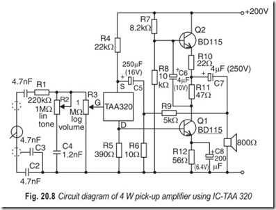
The transistors are connected in a single-ended class-A push-pull configuration. Since the output transistors are effectively in series for dc, a supply voltage of about 200 V is required. The drive signal for the upper transistor is obtained from the voltage drop across the collector resistor of the lower one.
The ac collector load is 800 Ω, so that either an 800 Ω loudspeaker, or an output transformer must be used. With the exception of the output stage, this circuit is similar to the 2W amplifier described earlier.
Performance Specifications (4 W Pickup Amplifier)
Nominal power output 4W into 800 Ω load
Sensitivity (1000 Hz) for Po = 4W 100 mV
(for minimum devices)
Frequency response (–3 db) 50 to 12,000 Hz
Total harmonic distortion at Po = 4W 5.5%
Voltage feedback factor 4 (typ).
Nominal supply voltage 200 V
Current consumption 72 mA (total).
The circuit diagram of a 4 W pickup amplifier using IC TAA 320 is giving Fig. 20.8.
THE CA810 INTEGRATED CIRCUIT
BEL CA810 is a monolithic audio power amplifier intended for use in stereo amplifies, tv receivers, radio receivers and other audio applications. The salient features of this device are :
● Large output current—7 W directly into 4 Ω load
● Low harmonic and crossover distortion.
● Operation over wide supply voltage range—4 V to 20 V, 2.5 A peak output current.
● Integral thermal limiting circuit, that shuts down the device in case of excessive package temperature.
● Minimal external components.
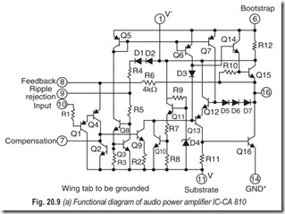
The functional diagram of CA810 is shown in Fig. 20.9(a). It contains a buffer, a preamplifier, a driver,a class ‘B’ output stage and a thermal limiting circuit. Emitter follower transistor Q1 forms the buffer stage and provides an input impedance of 5 MΩ. Transistor Q4, alongwith Q2, Q3 and Q8 constitutes the preamplifier. Q2, the active load of the preamplifiers Q4, forms a current mirror with Q3. Transistor Q8 provides the necessary base drive for the current mirror.
Transistors Q2, Q3 and Q8 form a closed loop and stabilise—the dc operating point of the preamplifier. The supply to the preamplifier is decoupled by a capacitor connected externally at the junction of R4 and R5. The above decoupling, in addition to reducing the noise in the preamplifier, prevents any output-input coupling through the power supply.
The output from the preamplifier is amplified by the transistor Q9 to a level sufficient to drive the output stage. The quasi-complementary output stage consists of a Darlington npn stage Q14 and Q15, and a simulated pnp stage Q13 and Q12. During the positive half cycle of the output, Q14 and Q15 conduct, sourcing current to the load. The Darlington pair, Q14 and Q15 has high input impedance and thus has negligible loading effect on the driver. This is further enhanced by ac feedback from the output to the collector of Q14 which is brought out as the bootstrap terminal. During negative half cycle, transistors Q13 and Q16 sink current from the load. Q12 provides the necessary sink current for transistor Q13. The output transistor pair is biased in class AB condition by diode D3 in the collector of driver transistor Q9. By sourcing constant current through D3 from the current source Q6, the quiescent current of the output stage is kept fairly constant. Q5, Q6 and Q7 form a current mirror and source currents to transistor Q8, driver transistor Q9, and base of Q12 respectively. The emitters of the current mirror transistors are tied to the bootstrap terminal so as to maintain the current through Q6 and Q7 constant, independent of the output swing. Resistor R6 provides the necessary d.c feedback for the amplifier. The junction of R6 and the emitter of the preamplifier transistor Q4 is brought out as the feedback terminal. The gain, and hence the sensitivity, of the amplifier can be varied by a suitable selection of resistors connected between output, feedback and ground terminals.
The thermal limiting network, incorporated in BEL CA-810, provides protection against damage due to excessive semiconductor temperature that may result from high ambient temperature and or excessive dissipation as encountered in sustained overloads. The thermal limiting feature automatically reduces the supply current and output power at high temperatures. Transistors Q10 and Q11 alongwith zener diode D4 form the thermal shutdown circuit. Any increase in the chip temperature increases breakdown voltage of the zener diode D4 and the voltage across R8. When the voltage across R8 rises to 0.6 V, transistor Q10, which is normally in ‘cut off’ condition, conducts, damps the collector of the driver transistor Q9 to ground and removes the drive to the output stages.
CA-810 offers a number of special advantages such as smaller size, low cost etc; compared to its discrete counterparts. CA-810 also offers to the circuit designers advantages like :
● Lesser constraints on the printed circuit board design as it needs very few additional discrete components.
● Good dc and ac circuit stability.
● Very low thermal drift—a result of its monolithic construction.
● No need of a matched output pair as the IC directly gives the required output.
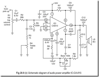
● The schematic diagram of audio power amplifier IC–CA-810 is given in Fig. 20.9(b)
THE BEL 700 INTEGRATED CIRCUIT
The monolithic integrated circuit BEL 700, in dual-in-line plastic package is designed for use in a.m. and AM/FM radio receivers. The IC design is aimed at maximum circuit flexibility combined with maximum economic suitablity. This versatile integrated circuit contains all the blocks that are required for an AM receiver except for the mixer/oscillator and the detector stages. Similarly for f.m. receiver, the tuner and the ratio detector are to be provided externally. This IC thus incorporates a two stage i.f. amplifier, an a.g.c. circuit, a preamplifier, a driver and a class B audio output stage with quiescent current stabilisation circuits. Novel internal stabilisation circuits ensure uniform sensitivity and very low crossover distortion over a wide supply voltage range from 2.7 volts to 12 volts.
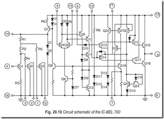
The internal circuit schematic of this IC is shown in Fig. 20.10. The IC consists of a high-frequency section comprising two amplifier stages with a.g.c. and an audio amplifier section. Only the latter section is dealt with in this paragraph.
The audio amplifier portion is designed for operation at nominal supply voltages of either 4.5 V or 6 V or 9 V. The preamplifier part of the audio amplifier consists of a differential amplifier comprising transistors Q4, Q5 and Q6.This stage is followed by two pnp transistors Q9 and Q10. D8 and D11 act as the current sinks for Q9 and Q10 respectively and a single ended drive signal is available at the collector of Q10. The output resistance of the drive signal, the parallel combination of collector resistances of Q10 and Q11, is sufficiently high for providing the necessary current drive for the output stage. Excessive overdrive for the stage is avoided by limiting the voltage in the positive direction by D10 and in the negative direction by Q11. Under nominal conditions the voltage at either terminals of D10 is equal to three diode drops. A positive overdrive makes the voltage at the anode of D10 to increase and D10 conducts diverting the excessive drive through itself. A negative overdrive, on the other hand, saturates transistor Q11 thus limiting the excessive drive to the output stage.
The output stage comprises of transistors Q13 to Q18. The configuration of this stage is so closed that a considerably larger part of the supply voltage is available for signal swing compared to normal output circuits. In the commonly used complementary Darligton output stages, the maximum amplitude of the output signal is equal to the supply voltage minus three VBE and two VCE (sat) drops. In this configuration, however, it is equal to the supply voltage minus one VBE and two VCE (sat) drops. This is an added advantage particularly at low operating voltages.
As Q14 and Q15 are lateral pnp devices their current gains in monolithic form cannot be controlled, and hence their gains in this circuit are swamped to unity by providing diodes across their base-emitter junctions. The bases of the two transistors Q13 and Q14 are tied together and the bias voltages are applied to their respective emitters. Transistors Q20 and Q22 are current sources controlled by Q21 and Q19. Q20 sources current through diodes D13 and D14 to the emitter of Q13 at a particular voltage, and similarly emitter of Q14 is biased by current source Q22.
The collector currents in Q13 and Q14 result in a quiescent current for Q16 and Q18 equal to Io. The biasing is independent of beta of the transistors, and the temperature compensation is perfect. The quiescent current Iq can be adjusted, through Q19, by an external resistance connected between terminal (7) and ground. The outputs of the current sources are controlled by the current determined by R8, diodes D11, D12 and the supply voltage.
PRACTICAL CIRCUITS USING IC-BEL 700
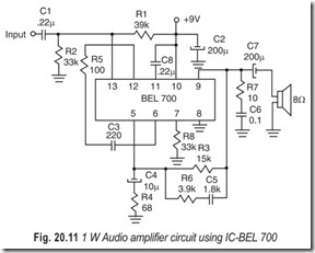
Figure 20.11 illustrates the circuit of a 1 watt audio amplifier using IC-BEL 700. When IC-BEL700 is used in audio applications, only the a.f. portion of the IC is utilised. This part of the IC contains an audio preamplifier, audio driver, stabilisation circuit for quiescent current and a class B output stage.
The class B audio output stage can provide a minimum power of 1 Ω into an 8 Ω load at 9 V; or 0.5 W into a 4 Ω load at 6 V; or 0.4 W into an 8 Ω load at 6 V; or 100 mW into a 4 Ω load at 3 V. This stage is designed to operate with a guaranteed minimum supply voltage at 2.7 volts and upto a maximum limit of 12 volts.
The audio input signal from the volume control is connected to non-inverting input terminal (13) of the IC. The dc potential at this point is maintained at almost half of the supply voltage by resistors R1 and R2. The potential at the output terminal (9) is thus held at half the supply voltage by the negative feedback provided by R3 connected between the input terminal (9) and the inverting input terminal (5). The inverting input terminal (5) is returned to ground for audio signals through C4 and R4. The ratio of R3 to R4 determines the overall closed loop gain of the audio stage. C5 controls the upper cut-off frequency of the amplifier, while C4 determines the lower cut off frequency. The R 5-C3 combination connected between terminals (6) and (12) rolls off the open loop frequency response above about 10 kHz at the rate of 6 dB per octave, thus ensuring stable operation of the amplifier. C8 connected between terminals (11) and (10) removes any h.f. noise present in the biasing arrangements within the IC, and C7 couples the output at terminal (9) to the load. The R7-C6 combination damps the rise in the impedance of the speaker at high frequencies and R8 at terminal (7) decides the quiescent current of the amplifier.
The circuit shown in Fig. 20.11 is particularly suitable for use in portable tape recorders.
THE CA-3020 INTEGRATED CIRCUIT
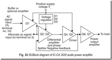
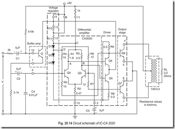
The operation of the CA-3020 can best be understood by considering its functional block diagram, shown in Fig 20.12. Transistor Q1 with the external 5.1 kΩ resistor constitutes an emitter-follower to provide an input resistance of 55 kΩ. The output of the buffer amplifier drives a differential amplifier which, with one base grounded (for a.c.), performs a phase splitting function to provide two signals 180° out of phase with each other at A and B, see Fig. 20.14. The voltage regulator, with the three diodes constructed from transistor base-emitter junctions and resistor R11, provides the differential amplifier with a collector supply voltage of about 2.1 volts at C and a base supply voltage of about 1.4 V at D.
The driver stage consists of two emitter followers, Q4 and Q5, whose collectors are supplied with full 9 V. Their outputs drive the power transistors, Q6 and Q7, connected in push-pull to a transformer external to the IC. Negative feedback from the outputs of Q4 and Q5, to the bases of transistors Q2 and Q3 through R5 and R7, respectively, is provided to help maintain the quiescent or idling currents through the driver and output transistors balanced and constant in the face of any imbalance that may occur in the chracteristics of the transistors or their loads. The balance may be enhanced by the inclusion of emitter resistors between terminals 5 and 6 and ground.
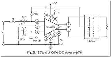
When properly heat-sinked the above audio amplifier will deliver one-half watt into a 3.2 Ω speaker with 35 mV applied. Since the CA3020 has an 8MHz bandwidth the possibility of oscillation can be minimised by restricting the overall bandwidth by adding bypass capacitor C4 and following good high-frequency wiring practices. The low-frequency response may be increased by increasing the values of C1, C2 and C3, while C4 is primarily responsible for establishing the upper frequency limit.
A practical application of IC-CA-3020 in an audio amplifier, based upon the previous discussion, is given in Fig. 20.13
GUITAR PREAMPLIFIER USING IC-LF536
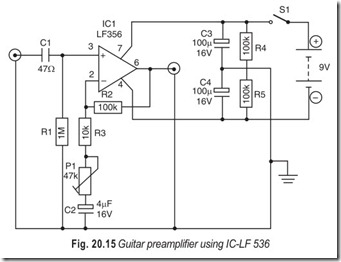
The output signal level provided by many electric guitars is not high enough to overdrive a valve amplifier. This overdriving is an essential part of the final guitar sound. The preamplifier circuit shown here boosts the guitar signal so that the input stage of the guitar amplifier is guaranteed to clip. As an aid to this the gain can be selected between three and eleven times.
The layout of the circuit is very simple. A single LF356, Fig. 20.15 provides the amplification, which is decided by the ratio of (R2 + R3 + P1) to (R3 + P1). The input impedance, which, at 1 MΩ, is quite high, is defined by R1 as the op-amp has f.e.t. inputs. This is a suitable impedance for most guitar pick-ups. A 9 V battery provides the power supply which is converted to a symmetrical + and – 4.5 V for the op-amp by means of R4, R5, C3, and C4. Current consumption is about 5 mA.
The circuit complete with battery, can easily be fitted into a small case. If a socket and plug are mounted in the case the preamplifier can simply be plugged into the guitar. If this is done, preset P1 can be replaced by an ordinary potentiometer so that the amplification can be controlled by means of a knob on the case.
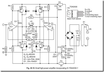
SMALL HIGH-POWER AMPLIFIER INCORPORATING IC-TDA2030
The TDA2030 is a complete amplifier contained in a single IC with a five pin-pentawatt package. Its class AB output stage can provide a power of 14 W into 4 Ω at a supply voltage of + 14 V.
The amplifier has a built-in short circuit and overload protection and also a thermal shutdown. This means that it is not so easy to destroy the IC as long as the supply voltage is kept below the absolute maximum of + 14 V.
Combining two 2030s with a few inexpensive power transistors can form an amplifier that can drive quite a lot of power into a load of 2 to 4 Ω. As illustrated in Fig. 20.16 the circuit is a standard ‘bridge’ amplifier. Each half of the bridge consists of a TDA2030 driving two complementary power transistors. The diodes D1 …… D4, are needed to protect the transistors from the loudspeaker coils inductive voltage. The gain of the whole amplifier is defined by :
A = 1 + (R 2/R 5) + (R 8/R 5)
With the values stated this works out at 32 db. If the gain is to be changed it must be remembered that R2 and R8 must have the same value.
The load on the amplifier may also be 2 Ω rather than the more normal 4 Ω, if power transistor stages are used. With a suitable power supply the amplifier can provide upto 200 Ω. Large heat sinks are essential, especially in this latter case. Distortion is less than 1% which is quite acceptable.
20 W + 20 W INTEGRATED STEREO AMPLIFIER
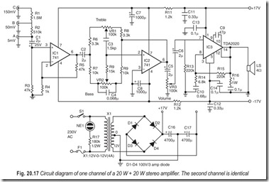
This stereo is built around integrated circuits only and does not employ any discrete transistors. A 741 op- amp is used in the preamplifier and active tone control. The power amplifier is built around IC-TDA2020. The use of ICs, especially in the power amplifier stage, simplifies construction.
The TDA 2020 integrated circuit features internal protection. No damage occurs if the output circuit is shorted. Since it also incorporates thermal protection, there is no danger of thermal runaway if excess power is dissipated in relation to the heat sink used. High temperatures cause the IC to shut down, but normal working is restored when the temperature falls. Both the channels are powered by the same dual power supply of + 17 V. The complete circuit diagram of the stereo amplifier (one channel) is shown in Fig. 20.17.
(1) Preamplifier: Input to the preamplifier is via a dc blocking capacitor C1. Resistor chain comprising R1, R2 and R3 forms an attenuator. The voltage across R3 is applied to IC1 input. The values of these resistors have been calculated such that the sensitivity is 5 mV in position A, 50mV in position B, and 150 mV in position C. Values of R1 and R2 can be altered to suit individual requirement of input sensitivity. The gain of the first stage is approximately fifty. The preamplifier does not provide any kind of equalisation, so tape head/magnetic phono inputs should be passed through suitable equalisers before feeding to this amplifier.
(2) Tone Control: Preamplifier output at pin 6 of IC1 is fed to tone control circuitry via C2. The tone control, being active type, gives both boost and cut off treble and bass. The circuit has almost unity gain throughout the audio range when bass and treble are set to their mid-way positions. The gain for a frequency of 1 kHz is unity at all settings of the tone controls. All other frequencies are boosted or cut as the controls are rotated. The performance characteristics of the tone control are :
Performance Characteristics
|
Output of the tone control is fed to volume control VR3 through C5. The signal level across VR3 will be around 240 mV for an input voltage of 5 mV across R3. There is no need for a balance control since each channel has a separate volume control.
(3) Power Amplifier: From VR3 coupling is by C6 to the input pin 7 of IC3. Negative feedback from the output (pin14) to the inverting input (pin8) is set by R14, R 15 and C10. The presence of C10 offers unity feedback at dc so as to keep output offset to a very small value. This enables direct coupling of the speakers to the output. R14 and C10 dictate the low-frequency roll-off characteristics. C9 is a frequency compensation capacitor. C13 and C14 are h.f. decoupling capacitors fitted very close to the pins of IC3.
The maximum supply of IC-TDA2020 is + 20 V. But this is not recommended as the IC may be damaged if higher voltage should arise and the power output obtained is 20 watts. With 8 Ω speaker and + 17 V supply, the output will be reduced to 13.5 watts.
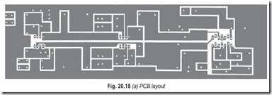
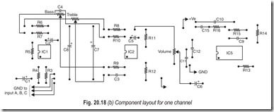
(4) Construction: The full size p.c.b. layout for one channel is shown in Fig 20.18. The same layout can be used for making a combined p.c.b. for both the channels, which will have a size of 22 cm by 13 cm. All components, except power supply and volume, treble and bass control pots, are soldered into the p.c.b.
It is preferable to assemble the low profile components—such as resistors, diodes and small capacitors- first, followed by ICs. Take care to see that all polarised components—such as diodes, electrolytic capacitors and integrated circuits—are mounted with correct orientation.
Before installing IC3, holes should be drilled in the p.c.b. to suit the heatsink used. In the prototype a solid aluminium heat sink of 8.5 cm length, 3 cm width and 2.2 cm height was used. It is important to note that C9 and a few resistors lie under the heatsink. Care should be taken to ensure that excepting the IC no component makes contact with the heatsink.
The heatsink mounting nut and bolt should be well isolated from the p.c.b. foil. In any case it should not make contact with the negative or positive rail of the supply or the earth (0 V). Before soldering IC3, the heat sink should be fixed. Apply a thin coat of heat sink compound (silicon grease) and mount the heatsink with suitable nuts and bolts. They should not make contact with chassis. After fixing the heatsink, IC3 can be soldered.
Suitable lengths of colour coded ribbon cable can be used for wiring volume and tone control pots. C4 is soldered over the bass control pot.
(5) Power Supply: The simplest part of this versatile amplifier is its power supply. It can be constructed without using a p.c.b.. The transformer used in the prototype had a secondary of 12–0–12 volts, rated at 4 amperes. For mono only the current rating can be halved. Silicon diodes of 3 amp and 100-volt reverse rating or a suitable bridge rectifier can be used. The transformer should be mounted away from input wiring side to keep the hum pick-up to a minimum.
The primary of the transformer is in series with the ON/OFF switch of the left channel volume control. Fuse F1 can be mounted in the back panel. A neon pilot lamp with a 180 kΩ resistor in series is connected across the primary of the transformer. The positive of the supply is connected to pin 1 of IC-3 and the negative to pins3 and 5. From p.c.b. earth (0 V) a thin wire (such as braid of a shielded wire) should be soldered to the nearest point in the chassis to the same earth point. The power supply common (0 V) should be properly soldered. Speaker sockets can be wired from pin14 of each TDA2020 and the chassis point where PCB is earthed. A common ground point will help to reduce ground loops, hum and instability problems.
(6) Input Wiring: From C1 and the nearest earth point (where R3 is earthed) a short length of shielded wire is connected to input socket A. R1 and R2 are wired in series with input sockets C and B respectively. The grounds of input sockets are earthed together with the braid of input shielded wire. Mounting should be in such a way that the sockets do not make contact with the chassis. For this RCA sockets mounted on a piece of bakelite sheet can be used. After completion of wiring, check for possible mistakes before switching on.
The p.c.b. can be assembled usings spacers and 1/8 size, 2.5 cm nuts and bolts. A cabinet for housing the stereo amplifier, measuring about 32 × 20 × 8 cm may be procured from the market.
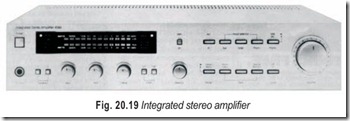
Integrated stereo amplifier is illustrated in Fig. 20.19
CONTROLS AND INDICATORS—FRONT PANEL
Pushbuttons:
STEREO/MONO MODE; INPUT SELECTORS (AUX, TUNER, PHONO); PHONE SELECTOR (MM/
MC). ACC (OUT/IN); Permits connection of signal processing accessory through rear jacks.
TAPE : Source/Monitor; recorder selector Loud; Connects loudness compensation to volume control circuit.
POWER : Turns power to amplifier on/off SPEAKERS: Two buttons, (A, B) FILTER: Two buttons (sub, High)
Knobs:
Tone Controls (Bass, Mid, Treble): Centre detented Balance: Centre detented
Volume:
Jack: PHONE
Indicators:
Input: Red for AUX, Tuner, Phono Tape.
SAFETY: Red Led flashes while amplifier protective system is operating. Power Output: Two parallel horizontal rows of fluorescent light segments. Readings from 0.0015 to 1.00 W and 0.15 to 100 W (autoranging). Peak hold for about 2 seconds.
Rear Apron
Phono jacks : L and R pairs for PHONO. TUNER, AUX input, Tape 1 REC and PLAY, TAPE 2 REC and PLAY, ACCESSORY IN and OUT.
Speakers : Insulated output connectors for two sets of speakers (A, B). AC Outlets: Three (Two switched.)
EXERCISES
Descriptive Questions
1. What are the advantages of integrated circuits over discrete components?
2. What are the fields of application of linear integrated circuits?
3. Explain the following :
(a) Differential voltage gain (b) Closed-loop gain
Fill in the Blanks
1. The differential amplifier is particularly suited to …………………………………………. technology .
2. Basically, a monolithic integrated circuit consists of a single…………………………………………. of silicon.
3. ICs may be packaged in circular metal can with up to …………………………………………. leads, in plastic in line packages with upto …………………………………………. leads, or in flat packages with over …………………………………………. leads.
4. General purpose operational amplifier with both …………………………………………. and inputs are now available.
5. An operational amplifier is a gain block with an …………………………………………. input impedance,…………………………………………. open loop gain, and a output impedance.
ANSWERS
Fill in the Blanks
|
1. integrated circuit |
2. chip |
3. 12, 16, 32 |
|
4. inverting, non-inverting |
5. infinite, zero |
