SOLID-STATE IMAGE SENSORS
Semiconductor-type image sensors are rugged and compact, with indefinite life and an ability to withstand mechanical shock and huge overloads of incident light – a direct view of the sun would write off any vidicon-type tube except the silicon-target variant, whereas a solid-state sensor would be unaffected.
In this ‘flat-plate’ system the photosensitive surface is not continuous; it is divided into hundreds of thousands of separate ‘islands’ of silicon photodiodes arranged in horizontal rows to conform with the television scanning lines themselves.
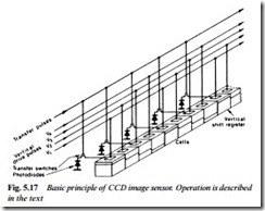
Each photodiode consists of a single picture element, and during the 20 ms field period it builds up a voltage charge proportional to the light falling on it. Each photodiode cathode has its own MOS- FET transistor switch, as shown in Fig. 5.17. When a pulse is applied to the transistor gate the diode’s charge is transferred to a shift register. Unlike a digital shift register the type used in a solid-state image sensor can deal with an analogue signal which in effect consists of ‘packets’ of electrons. It is known as a bucket-brigade device (BBD) and finds applications elsewhere in consumer electronics, primarily for analogue delay lines.
The charge packets are stepped along the register by sequentially changing the voltages applied to the BBD’s cells. The electron charges readily fall into an adjacent ‘potential well’, and by setting up progressively deeper depletion layers in adjacent cells they can be stepped along the shift register/BBD by means of clock pulses in a four- phase sequence.
photodiodes has its own vertical shift register. During each field blanking period a transfer pulse is applied to the gate of each FET to switch the charges accumulated in each photodiode into the adjacent shift register. All the FETs are simultaneously pulsed, so that once per TV field a complete set of pixel charges is transferred. On the first change of V-clock pulse the charges in all the vertical shift registers hop one cell upwards. At the top of the array is a horizontal shift register, into which is now loaded the topmost line of the picture. This is another BBD, whose contents are continually and rapidly transferred towards the left by the same ‘progressive well’ technique as used in the vertical shift registers, using the same four- phase sequence of transfer pulses. For this register the pulse rate is much faster: the readthrough here is at picture-element rate, in practice about 8 MHz. The charge packets roll off the left-hand end of the horizontal shift register in the form of a series of pulses of varying height: an analogue video signal. Before it can be used the clock pulses and switching hash must be filtered out.
At each line blanking interval the vertical registers are pulsed to transfer complete picture lines into the horizontal BBD at 64 μs intervals, where each is clocked leftwards during the next line scan period. The serial information stream corresponds to the target output of a conventional vidicon tube. At the end of each field the charges from all the photodiodes have been read out, the vertical and
horizontal BBDs are empty, and the whole sequence is repeated for the next field.
The CCD clock and drive pulses are generated in a timing/divider IC governed by the camera’s master sync and subcarrier generator section (SSG), which is itself paced by a precision crystal.
Colour CCDs
The CCD image sensor described above produces a monochrome picture; each photodiode’s charge is proportional to the luminance value of the pixel it represents. As with tubes, high-quality broadcast and professional cameras use three sensors, one for each primary colour, and the incoming light path is optically split and filtered. For consumer cameras this approach is very expensive, so single-array colour CCD image sensors have been developed with colour-filter matrices bonded to the faceplate and aligned with the photocell array. They work on similar principles to the ones described in this chapter (Figs 5.12 and 5.16) and the next.
Fast shutter
Like vidicon tubes, the CCD array builds up a charge throughout the field period, with each pixel integrating the light falling on it for about 19 ms. The storage effect of this exposure time gives good sensitivity, particularly important in low-light conditions. If, however, anything in the picture moves appreciably during this 19 ms period, it is displayed (during still-frame reproduction) as a blur. With a CCD image sensor it is possible to separate the ‘scanning’ and ‘storage’ functions to give a fast shutter effect.
Towards the end of the field period a special transfer pulse is applied to dump the photodiodes’ charges into the vertical shift registers. It is shortly followed by a high-speed pulse train through all the vertical registers to ‘flush’ them. The effect of this is not vis- ible because the video signal is muted at this time: the process takes place during the vertical blanking period. A short period (set by the user’s shutter speed control) is afforded to the photodiodes to charge from incoming light, then once more a transfer pulse is applied to pass the charges into the vertical shift register. The brightness information acquired during this limited exposure is stepped along the registers in the normal way to form the video output signal, which appears continuous because of the storage capability of the cells in the BBD shift registers.
The penalty for fast-shutter operation, as with conventional photography, is a loss of sensitivity, calling for an increase in light level or a large aperture setting. A range of shutter speeds is provided to trade off sensitivity against blur effects, the fastest of which is only suitable for use in bright outdoor situations. Even in good light, however, fast shutter settings should only be used when freeze-frame or slow-motion analysis of the event is likely to be needed.

