fuse What It Does, How It Works ,Values ,Variants ,How to Use it and How to Use it

What It Does

A fuse protects an electrical circuit or device from excessive current when a metal element inside it melts to create an open circuit. With the excep­tion of resettable fuses (discussed separately in “Resettable Fuses” (page 24)), a fuse must be dis­ carded and replaced after it has fulfilled its function.

When high current melts a fuse, it is said to blow or trip the fuse. (In the case of a resettable fuse, only the word trip is used.)

A fuse can work with either AC or DC voltage, and can be designed for almost any current. In resi­dential and commercial buildings, circuit break­ ers have become common, but a large cartridge fuse may still be used to protect the whole sys­ tem from short-circuits or from overcurrent caused by lightning strikes on exposed power lines.

In electronic devices, the power supply is al­ most always fused.

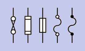
Schematic symbols for a fuse are shown in Figure 4-1. Those at the right and second from right are most frequently used. The one in the center is approved by ANSI, IEC, and IEEE but is seldom seen. To the left of that is the fuse symbol understood by electrical contractors in architec­tural plans. The symbol at far left used to be com­mon but has fallen into disuse.

clip_image003

How It Works

The element in a fuse is usually a wire or thin metal strip mounted between two terminals. In a car­tridge fuse, it is enclosed in a glass or ceramic cylinder with a contact at each end, or in a small metallic can. (Old-style, large, high-amperage fuses may be packaged in a paper or cardboard tube.) The traditional glass cartridge allows vis­ual inspection to confirm that the fuse has blown.

A fuse responds only to current, not to voltage. When choosing a fuse that will be reliable in con­ditions of steady current consumption, a safe rule is to figure the maximum amperage when all components are functioning and add 50%. How­ ever, if current surges or spikes are likely, their duration will be relevant. If I is the current surge

in amps and t is its duration in seconds, the surge sensitivity of a fuse—which is often referred to verbally or in printed format as I2t—is given by the formula:

I2t = I2 * t

Some semiconductors also have an I2t rating, and should be protected with a similarly rated fuse.

Any fuse will present some resistance to the cur­ rent flowing through it. Otherwise, the current would not generate the heat that blows the fuse. Manufacturer datasheets list the voltage drop that the internal resistance of a fuse is likely to introduce into a circuit.

Values

The current rating or rated current of a fuse is usually printed or stamped on its casing, and is the maximum flow that it should withstand on a continuous basis, at the ambient temperature specified by the manufacturer (usually 25 degrees Centigrade). The ambient temperature refers to the immediate environment of the fuse, not the larger area in which it may be located. Note that in an enclosure containing other components, the temperature is usually significantly higher than outside the enclosure.

Ideally a fuse should function reliably and indefinitely at its rated maximum amperage, but should blow just as reliably if the current rises by approximately 20% beyond the maximum. In re­ ality, manufacturers recommend that continuous loading of a fuse should not exceed 75% of its rating at 25 degrees Centigrade.

The voltage rating or rated voltage of a fuse is the maximum voltage at which its element can be counted on to melt in a safe and predictable manner when it is overloaded by excess current. This is sometimes known as the breaking capaci­ty. Above that rating, the remaining pieces of the fuse element may form an arc that sustains some electrical conduction.

A fuse can always be used at a lower voltage than its rating. If it has a breaking capacity of 250V, it will still provide the same protection if it is used at 5V.

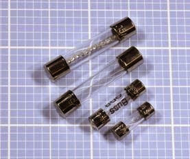
Four differently rated glass cartridge fuses are shown in Figure 4-2. The one at the top is a slow- blowing type, rated at 15A. Its element is de­ signed to absorb heat before melting. Below it is a 0.5A fuse with a correspondingly thinner ele­ment. The two smaller fuses are rated at 5A each. The center two fuses have a maximum voltage rating of 250V, while the one at the top is rated at 32V and the one at the bottom is rated at 350V. Clearly, the size of a fuse should never be used as a guide to its ratings.

clip_image005

Figure 4-2. Four glass cartridge fuses. See text for de- tails.

clip_image001[1]Variants

Early power fuses in residential buildings consisted of bare nichrome wire wrapped around a porcelain holder. In the 1890s, Edison developed plug fuses in which the fuse was contained in a porcelain module with a screw thread, compatible with the base of an incandescent bulb. This design persisted in some U.S. urban areas for more than 70 years, is still found in old buildings, and is still being manufactured.

Small Cartridge Fuses

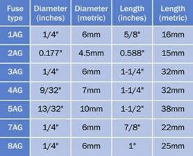
Small cartridge fuses for appliances and electronics equipment such as those shown in Figure 4-2–are available in sizes tabulated in Figure 4-3. With the exception of the 4.5mm diameter fuse (a European addition), these sizes were originally measured in inches; today, they are often described only with the equivalent metric measurement. Any cartridge fuse is usually available with the option of a lead attached to it at each end, so that it can be used as a through-hole component.

clip_image007

Figure 4-3. The approximate physical sizes of commonly used small glass or ceramic cartridge fuses are shown here with the codes that are often used to identify them.

Fuses may be fast acting, medium acting, or slow- blowing, the last of which may alternatively be referred to as delay fuses. Extra-fast–acting fuses are available from some manufacturers. The term SloBlo is often used but is actually a trademark of Littelfuse. None of the terms describing the speed of action of a fuse has been standardized with a specific time or time range.

Some cartridge fuses are available in a ceramic format as an alternative to the more common glass cylinder. If accidental application of extremely high current is possible (for example, in a multimeter that can be set to measure amps, and may be accidentally connected across a powerful battery), a ceramic cartridge is prefera­ble because it contains a filler that will help to stop an arc from forming. Also, if a fuse is physically destroyed by application of very high cur­ rent, ceramic fragments may be preferable to glass fragments.

Automotive fuses are identifiable by their use of blades designed for insertion in flat sockets where the fuse is unlikely to loosen as a result of vibration or temperature changes. The fuses come in various sizes, and are uniformly color- coded for easy identification.

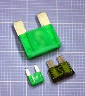
A selection of automotive fuses is shown in Figure 4-4. The type at the top is typically de­ scribed as a “maxi-fuse” while the type at bottom-left is a “mini-fuse.” Here again, size is ir­ relevant to function, as all three of those pictured are rated 30A at 32V.

clip_image009

Figure 4-4. Three automotive fuses. All have the same rating: 30A at 32V.

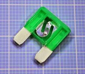
In Figure 4-5, the largest of the fuses from Figure 4-4 has been cut open to reveal its ele­ment.

clip_image011

Figure 4-5. The largest fuse from the previous figure, cut open to reveal its element.

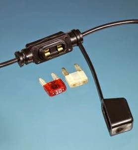
Usually automotive fuses are mounted together in a block, but if aftermarket accessory equip­ment is added, it may be protected by an inline fuse in a holder that terminates in two wires. This is shown with two sample fuses in Figure 4-6. Similar inline fuse holders are manufactured for other types of fuses.

Strip Fuses

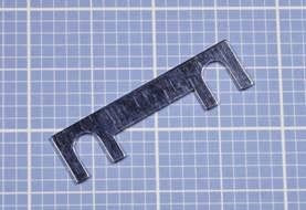
High-amperage fuses for vehicles may be sold in “strip fuse” format, also known as a fusible link, designed to be clamped between two screw- down terminals. Since some jumpers may look very similar, it is important to keep them sepa­rate. A strip fuse is shown in Figure 4-7.

Through-Hole Fuses

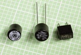
Small fuses with radial leads, which seem appro­priate for through-hole insertion in printed cir­cuit boards, are actually often used in conjunc­tion with appropriate sockets, so that they can be easily replaced. They are described in cata­logues as “subminiature fuses” and are typically found in laptop computers and their power sup­ plies, also televisions, battery chargers, and air conditioners. Three examples are shown in Figure 4-8. All have slow-blowing characteristics.

clip_image013

Figure 4-6. Two blade-type fuses, commonly used for automotive applications, shown with an inline fuse holder. The plastic cap, at right, is closed over the holder when a fuse has been installed.

clip_image015

Figure 4-7. This strip fuse is intended for use in diesel vehicles. The example shown is rated 100A at 36V.

Resettable Fuses

Properly known as a polymeric positive tempera­ture coefficient fuse (often abbreviated PTC or PPTC), a resettable fuse is a solid-state, encapsu­lated component that greatly increases its resist­ ance in response to a current overload, but grad­ually returns to its original condition when the flow of current is discontinued. It can be thought

clip_image017

Figure 4-8. Three subminiature fuses terminating in wire leads. From left to right: 10A at 250V, 2.5A at 250V, and 5A at 250V.

of as a thermistor that has a nonlinear response. Three through-hole examples are shown in Figure 4-9. While different sizes of cartridge fuse may share the same ratings, differently rated re­ settable fuses may be identical in size. The one on the left is rated 40A at 30V, while the one on the right is rated 2.5A at 30V. (Note that the codes printed on the fuses are not the same as their manufacturer part numbers.) The fuse at the top is rated 1A at 135V.

When more than the maximum current passes through the fuse, its internal resistance increases suddenly from a few ohms to hundreds of thou­ sands of ohms. This is known as tripping the fuse. This inevitably entails a small delay, but is com­ parable to the time taken for a slow-blowing fuse to respond.

A resettable fuse contains a polymer whose crys­talline structure is loaded with graphite particles that conduct electricity. As current flowing through the fuse induces heat, the polymer transitions to an amorphous state, separating the graphite particles and interrupting the conduc­tive pathways. A small current still passes through the component, sufficient to maintain its amorphous state until power is disconnected.
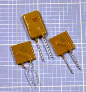
clip_image019Figure 4-9. Some through-hole resettable fuses. See text for details.

After the resettable fuse cools, it gradually re­ crystallizes, although its resistance does not fall back completely to its original value for more than an hour.

The maximum safe level of current for a resetta­ble fuse is known as the hold current, while the current that triggers its response is termed the trip current. Resettable fuses are available with trip-current ratings from 20mA to 100A. While conventional appliance and electronics fuses may be rated as high as 600V, resettable fuses are seldom rated above 100V.

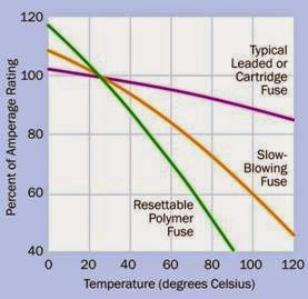
Typical cartridge fuses are affected only to a mi­ nor extent by temperature, but the current rating of a resettable fuse may diminish to 75% of its normal value at 50 degrees Centigrade and may drop to 50% of its normal value at 80 degrees Centigrade. In other words, a fuse that is rated for 4A at 25 degrees may tolerate a maximum of only 3A when it operates at twice that temperature. See Figure 4-10.

How to Use it

clip_image021

Figure 4-10. The three curves give a very approximate idea of the temperature sensitivity of three types of fuses commonly used to protect electronic equipment. The left- hand scale provides an approximate value for the amperage which will trip the fuse. Figure 4-11. A surface-mount resettable fuse. See text for

details.

Conventional slow-blowing fuses are temperature-sensitive, but to a lesser degree than resettable fuses.

Resettable fuses are used in computer power supplies, USB power sources, and loudspeaker enclosures, where they protect the speaker coils from being overdriven. They are appropriate in situations where a fuse may be tripped relatively often, or where technically unsophisticated users may feel unable to replace a fuse or reset a circuit breaker.

Brand names for resettable fuses include Poly­ Switch, OptiReset , Everfuse, Polyfuse, and Multi­ fuse. They are available in surface-mount (SMT) packages or as through-hole components, but not in cartridge format.

Surface Mount Fuses

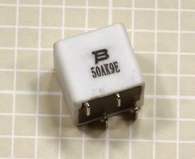
Because surface-mount fuses are difficult or im­possible to replace after they have been soldered onto the board, they are often resettable.A surface-mount resettable fuse approximately 0.3” square is shown in Figure 4-11. It is rated for 230V and has an internal resistance of 50 ohms. Its hold current is 0.09A and its trip current is 0.19A.

clip_image023

Figure 4-11. A surface-mount resettable fuse. See text for details.


How to Use it

Any equipment that may be plugged into a wall outlet should be fused, not only to protect its components but also to protect users who may open the box and start investigating with a screwdriver.

Equipment that contains powerful motors, pumps, or other inductive loads should be pro­tected with slow-blowing fuses, as the initial surge of current when the equipment is switched on is likely to rise well above the rating of the fuse. A slow-blowing fuse will tolerate a surge for a couple of seconds. Other fuses will not.

Conversely, fast-acting fuses should be used with electronic equipment, especially integrated cir­cuits that are quickly and easily damaged.

Any device using substantial battery power should be fused because of the unpredictable and generally bad behavior of batteries when they are short-circuited. Parallel connections be­ tween multiple large batteries should be fused

26 Encyclopedia of Electronic Components Volume 1

power > connection > fuse What Can Go Wrong

to avoid the possibility that a highly charged bat­tery may attempt to recharge its neighbor(s). Large “J size” fuses rated from 125A to 450A have become common in the solar power community, where banks of lead-acid batteries are often used. These fuses have a thick brass tab at each end, drilled so that they can be bolted into place. Alternatively, they will push-fit into an appropri­ ate fuseholder.

For cartridge fuses up to 1/4” in diameter that don’t have leads attached, appropriately sized fuseholders are available in several formats:

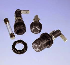
Panel mounted fuse enclosure is probably the most common, consisting of a plastic tube with a spring-contact at the bottom, and a plastic cap with a second contact inside. The cap either screws onto the tube of the fuse, or is pushed down and turned to hold it in place. A nut is pro­ vided to secure the fuseholder after it has been inserted into a hole drilled in the panel. The fuse is dropped into the tube, and the cap is applied. This type of holder is available in full-length or shorter, “low profile” formats. A low-profile hold­ er is shown in Figure 4-12. It is shown assembled at right, with its component parts disassembled alongside.

clip_image026

Figure 4-12. A low-profile panel-mounted fuse holder shown disassembled (left) and assembled (right).

Circuit board mounted fuse enclosure is ba­sically the same as the panel-mounted version, but with through-hole solder pins attached.

Fuse block is a small plastic block with two clips on its upper surface for insertion of a cartridge fuse.

Fuse clips can be bought individually, with sol­ der pins for through-hole mounting.

Inline fuse holder is designed to be inserted in a length of wire. Usually made of plastic, it will either terminate it, wires or will have metal con­ tacts to crimp or solder at each end. See Figure 4-6.

Through-hole fuse holders are available for subminiature fuses.

What Can Go Wrong
Repeated Failure

When a fuse in a circuit blows frequently, this is known as nuisance opening. Often it can result from failure to take into account all the aspects of the circuit, such as a large filtering capacitor in a power supply that draws a major surge of cur­ rent when the power supply is switched on. The formally correct procedure to address this prob­lem is to measure the power surge, properly known as peak inrush current, with an oscillo­scope, calculate the I2 * t of the wave form, and select a fuse with a rating at least 5 times that value.

A fuse should never be replaced with anequiva ­lent length of wire or any other conductor.

Soldering Damage

When a through-hole or surface-mount fuse is soldered into place, heat from the soldering pro­cess can cause the soft metal element inside the fuse to melt partially and reflow. This is likely to change the rating of the fuse. Generally, fuses should be treated with the same caution as sem­iconductors when they are fixed in place with solder.

Placement

A fuse should be placed close to the power source or power input point in a circuit, so that it protects as much of the circuit as possible.
 

battery What It Does,How It Works,Variants,Values,How to Use it and What Can Go Wrong

This entry covers electrochemical power sources. Electricity is most often generated ectromagnetically, but since these sources cannot be classified as components, they are outside the scope of the encyclopedia. Electrostatic sources are excluded for similar reasons.

A battery is sometimes referred to as a cell or power cell, but can actually contain multiple cells, as defined in this entry. It used to be called an accumulator or a pile, but those terms are now archaic.

What It Does

A battery contains one or more electrochemical cells in which chemical reactions create an elec­trical potential between two immersed termi­nals. This potential can be discharged as current passing through a load.

An electrochemical cell should not be confused with an electrolytic cell, which is powered by an external source of electricity to promote electrol­ysis, whereby chemical compounds are broken down to their constituent elements. An electro­ lytic cell thus consumes electricity, while an elec­trochemical cell produces electricity.

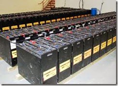
Batteries range in size from button cells to large lead-acid units that store power generated by solar panels or windmills in locations that can be off the grid. Arrays of large batteries can provide bridging power for businesses or even small communities where conventional power is un­ reliable. Figure 2-1 shows a 60KW, 480VDC self- watering battery array installed in a corporate data center, supplementing wind and solar sour­ces and providing time-of-day peak shaving of energy usage. Each lead-acid battery in this array measures approximately 28” × 24” × 12” and weighs about 1,000 lb.

clip_image003

Figure 2-1. A battery array providing 60KW at 480VDC as backup for a corporate data center. (Photo by permission of Hybridyne Power Systems, Canada, Inc., and the Hy- bridyne group of companies. Copyright by Hybridyne, an internationally registered trademark of Hybridyne Power Systems Canada Inc. No right of further reproduction un- less specifically granted by Hybridyne.)

How It Works

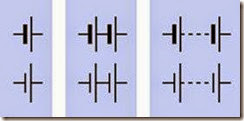
Schematic symbols for a battery are shown in Figure 2-2. The longer of the two lines represents the positive side of the battery, in each case. One way to remember this is by imagining that the longer line can be snipped in half so that the two segments can combine to form a + sign. Tradi­tionally, multiple connected battery symbols in­ dicate multiple cells inside a battery; thus the center symbols in the figure could indicate a 3V battery, while those on the right would indicate a voltage greater than 3V. In practice, this con­ vention is not followed conscientiously.

clip_image005

Figure 2-2. Schematic symbols for a battery. Each pair of symbols within a blue rectangle is functionally identical.

clip_image006How It Works

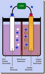
In a basic battery design often used for demon­ stration purposes, a piece of copper serves as an electrode, partially immersed in a solution of cop­ per sulfate, while a piece of zinc forms a second electrode, partially immersed in a solution of zinc sulfate. Each sulfate solution is known as an elec­ trolyte, the complete battery may be referred to as a cell, and each half of it may be termed a half- cell.

A simplified cross-section view is shown in Figure 2-3. Blue arrows show the movement of electrons from the zinc terminal (the anode), through an external load, and into a copper ter­ minal (the cathode). A membrane separator al­ lows the electrons to circulate back through the battery, while preventing electrolyte mixing.

Orange arrows represent positive copper ions. White arrows represent positive zinc ions. (An ion is an atom with an excess or deficit of electrons.) The zinc ions are attracted into the zinc sulfate electrolyte, resulting in a net loss of mass from the zinc electrode.

Meanwhile, electrons passing into the copper electrode tend to attract positive copper ions, shown as orange arrows in the diagram. The cop­ per ions are drawn out of the copper sulfate elec­ trolyte, and result in a net accumulation of cop­ per atoms on the copper electrode.

This process is energized partially by the fact that zinc tends to lose electrons more easily than cop­ per.

clip_image008

Figure 2-3. A classically simple electrochemical cell. See text for additional details.

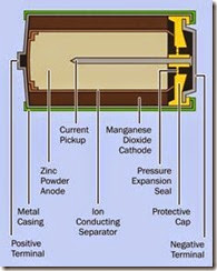
Batteries for use in consumer electronics typical­ ly use a paste instead of a liquid as an electrolyte, and have been referred to as dry cells, although this term is becoming obsolete. The two half- cells may be combined concentrically, as in a typical 1.5-volt C, D, AA, or AAA alkaline battery (see Figure 2-4).

clip_image010

Figure 2-4. Cross-section view of a typical 1.5-volt alka- line battery.

A 1.5V battery contains one cell, while a 6V or 9V battery will contain multiple cells connected in series. The total voltage of the battery is the sum of the voltages of its cells.

Electrode Terminology

The electrodes of a cell are often referred to as the anode and the cathode. These terms are con­ fusing because the electrons enter the anode in­ side the cell and leave it outside the cell, while electrons enter the cathode from outside the celland leave it inside the cell. Thus, the anode is an electron emitter if you look at it externally, but the cathode is an electron emitter if you look at it internally.

Conventional current is imagined to flow in the opposite direction to electrons, and therefore, outside the cell, this current flows from the cath­ ode to the anode, and from this perspective, the cathode can be thought of as being “more posi­ tive” than the anode. To remember this, think of the letter t in “cathode” as being a + sign, thus: ca+hode. In larger batteries, the cathode is often painted or tagged red, while the anode may be painted or tagged black or blue.

When a reusable battery is recharged, the flow of electrons reverses and the anode and the cath­ ode effectively trade places. Recognizing this, the manufacturers of rechargeable batteries may refer to the more-positive terminal as the anode. This creates additional confusion, exacerbated further still by electronics manufacturers using the term “cathode” to identify the end of a di­ ode which must be “more negative”(i.e., at a low­ er potential) than the opposite end.

To minimize the risk of errors, it is easiest to avoid the terms “anode” and “cathode” when referring to batteries, and speak instead of the negative and positive terminals. This encyclopedia uses the common convention of reserving the term “cathode” to identify the “more negative” end of any type of diode.

Variants

Three types of batteries exist.

1.Disposable batteries, properly (but infre­quently) referred to as primary cells. They are not reliably rechargeable because their chemical reactions are not easily reversible.

2.Rechargeable batteries, properly (but in fre­quently) known as secondary cells. They can be recharged by applying a voltage between

the terminals from an external source such as a battery charger. The materials used in the battery, and the care with which the battery is maintained, will affect the rate at which chemical degradation of the electrodes gradually occurs as it is recharged repeated­ ly. Either way, the number of charge/ discharge cycles is limited.

1. Fuel Cells require an inflow of a reactive gas such as hydrogen to maintain an electro­ chemical reaction over a long period. They are beyond the scope of this encyclopedia.

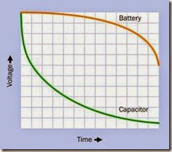
A large capacitor may be substituted for a bat­ tery for some applications, although it has a low­ er energy density and will be more expensive to manufacture than a battery of equivalent power storage. A capacitor charges and discharges much more rapidly than a battery because no chemical reactions are involved, but a battery sustains its voltage much more successfully dur­ ing the discharge cycle. See Figure 2-5.

clip_image012

Figure 2-5. The voltage drop of a discharging capacitor is much steeper initially than that of a battery, making ca- pacitors unsuitable as a battery substitute in many appli- cations. However, the ability of a capacitor to discharge very rapidly at high amperage can sometimes be a signifi- cant advantage.

Disposable Batteries

The energy density of any disposable battery is higher than that of any type of rechargeable bat­ tery, and it will have a much longer shelf life be­ cause it loses its charge more slowly during stor­ age (this is known as the self-discharge rate). Dis­ posable batteries may have a useful life of five years or more, making them ideal for applica­ tions such as smoke detectors, handheld re­ motes for consumer electronics, or emergency flashlights.

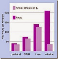
Disposable batteries are not well suited to deliv­ ering high currents through loads below 75Ω. Rechargeable batteries are preferable for higher- current applications. The bar chart in Figure 2-6 shows the rated and actual capabilities of an al­ kaline battery relative to the three most com­ monly used rechargeable types, when the bat­ tery is connected with a resistance that is low enough to assure complete discharge in 1 hour.

The manufacturer’s rating of watt hours per kilo is typically established by testing a battery with a relatively high-resistance load and slow rate of discharge. This rating will not apply in practice if a battery is discharged with a C-rate of 1, mean­ ing complete discharge during 1 hour.

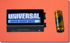
Common types of disposable batteries are zinc- carbon cells and alkaline cells. In a zinc-carbon cell, the negative electrode is made of zinc while the positive electrode is made of carbon. The limited power capacity of this type of battery has reduced its popularity, but because it is the cheapest to manufacture, it may still be found where a company sells a product with “batteries included.” The electrolyte is usually ammonium chloride or zinc chloride. The 9V battery in Figure 2-7 is actually a zinc-carbon battery ac­ cording to its supplier, while the smaller one be­ side it is a 12V alkaline battery designed for use in burglar alarms. These examples show that bat­ teries cannot always be identified correctly by a casual assessment of their appearance.

clip_image014

Figure 2-6. Because of their relatively high internal resist- ance, alkaline batteries are especially unsuited to high dis- charge rates, and should be reserved for applications where a small current is required over a long period. (Chart derived from http://batteryuniversity.com.)

clip_image016

Figure 2-7. At left, a cheap carbon-zinc battery; at right, a 12V alkaline burglar-alarm battery. See text for additional details.

In an alkaline cell, the negative electrode is made of zinc powder, the positive electrode is manga­ nese dioxide, and the electrolyte is potassium hydroxide. An alkaline cell may provide between three to five times the power capacity of an equal size of zinc-carbon cell and is less susceptible to voltage drop during the discharge cycle.

Extremely long shelf life is necessary in some military applications. This may be achieved by using a reserve battery, in which the internal chemical compounds are separated from each other but can be recombined prior to use.

Rechargeable Batteries

Commonly used types are lead-acid, nickel cad­ mium (abbreviated NiCad or NiCd), nickel-metal hydride (abbreviated NiMH), lithium-ion (abbreviated Li-ion), and lithium-ion polymer.

Lead-acid batteries have existed for more than a century and are still widely used in vehicles, bur­ glar alarms, emergency lighting, and large power backup systems. The early design was described as flooded; it used a solution of sulfuric acid (generically referred to as battery acid) as its electro­ lyte, required the addition of distilled water periodically, and was vented to allow gas to escape. The venting also allowed acid to spill if the bat­ tery was tipped over.

The valve-regulated lead-acid battery (VRLA) has become widely used, requiring no addition of water to the cells. A pressure relief valve is in­ cluded, but will not leak electrolyte, regardless of the position of the battery. VRLA batteries are preferred for uninterruptible power supplies for data-processing equipment, and are found in automobiles and in electric wheelchairs, as their low gas output and security from spillage increases their safety factor.

VRLA batteries can be divided into two types: absorbed glass mat (AGM) and gel batteries. The electrolyte in an AGM is absorbed in a fiber-glass mat separator. In a gel cell, the electrolyte is mixed with silica dust to form an immobilized gel.

The term deep cycle battery may be applied to a lead-acid battery and indicates that it should be more tolerant of discharge to a low level—per­ haps 20 percent of its full charge (although man­ ufacturers may claim a lower number). The plates in a standard lead-acid battery are composed of a lead sponge, which maximizes the surface area available to acid in the battery but can be phys­ically abraded by deep discharge. In a deep cycle battery, the plates are solid. This means they are more robust, but are less able to supply high am­ perage. If a deep-discharge battery is used to start an internal combustion engine, the battery should be larger than a regular lead-acid battery used for this purpose.

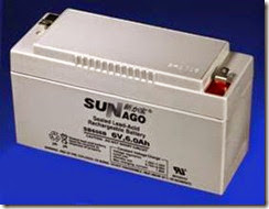
A sealed lead-acid battery intended to power an external light activated by a motion detector is shown in Figure 2-8. This unit weighs several pounds and is trickle-charged during the day­ time by a 6” × 6” solar panel.

clip_image018

Figure 2-8. A lead-acid battery from an external light ac- tivated by a motion sensor.

Nickel-cadmium (NiCad) batteries can withstand extremely high currents, but have been banned in Europe because of the toxicity of metallic cad­ mium. They are being replaced in the United States by nickel-metal hydride (NiMH) types, which are free from the memory effect that can prevent a NiCad cell from fully recharging if it has been left for weeks or months in a partially dis­ charged state.

Lithium-ion and lithium-ion polymer batteries have a better energy-to-mass ratio than NiMH batteries, and are widely used with electronic devices such as laptop computers, media play­ ers, digital cameras, and cellular phones. Large arrays of lithium batteries have also been used in some electric vehicles.

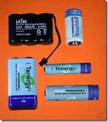
Various small rechargeable batteries are shown in Figure 2-9. The NiCad pack at top-left was manufactured for a cordless phone and is rapidly becoming obsolete. The 3V lithium battery at top-right was intended for a digital camera. The three batteries in the lower half of the photo­ graph are all rechargeable NiMH substitutes for 9V, AA, and AAA batteries. The NiMH chemistry results in the AA and AAA single-cell batteries being rated for 1.2V rather than 1.5V, but the manufacturer claims they can be substituted for 1.5V alkaline cells because NiMH units sustain their rated voltage more consistently over time. Thus, the output from a fresh NiMH battery may be comparable to that of an alkaline battery that is part-way through its discharge cycle.

clip_image020

Figure 2-9. Top left: NiCad battery pack for a cordless phone. Top right: Lithium battery for a digital camera. The other batteries are rechargeable NiMH substitutes for ev- eryday alkaline cells.

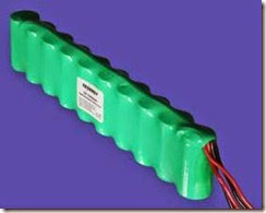
NiMH battery packs are available to deliver sub­ stantial power while being smaller and lighter than lead-acid equivalents. The NiMH package in Figure 2-10 is rated for 10Ah, and consists of ten

D-size NiMH batteries wired in series to deliver 12VDC. This type of battery pack is useful in ro­ botics and other applications where a small motor-driven device must have free mobility.

clip_image022

Figure 2-10. This NiMH battery pack is rated at 10Ah and delivers 12 volts from ten D-size cells wired in series.

Values
Amperage

The current delivered by a battery will be largely determined by the resistance of the external load placed between its terminals. However, because ion transfer must occur inside the battery to complete the circuit, the current will also be limi­ ted by the internal resistance of the battery. This should be thought of as an active part of the cir­ cuit.

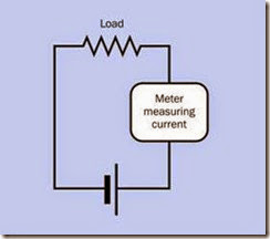
Since a battery will deliver no current if there is no load, current must be measured while a load is attached, and cannot be measured by a meter alone. The meter will be immediately overloa­ ded, with destructive results, if it is connected directly between the terminals of a battery, or in parallel with the load. Current must always be measured with the meter in series with the load, and the polarity of the meter must correspond with the polarity of the battery. See Figure 2-11.

clip_image024

Figure 2-11. When measuring current using an ammeter (or a multimeter configured to measure amps), the meter must be placed in series with the battery and a load. To avoid damaging the meter, it must never be applied di- rectly across the terminals of the battery, or in parallel with a load. Be careful to observe the polarity of the meter.

Capacity

The electrical capacity of a battery is measured in amp-hours, abbreviated Ah, AH, or (rarely) A/H. Smaller values are measured in milliamp-hours, usually abbreviated mAh. If I is the current being drawn from a battery (in amps) and T is the time for which the battery can deliver that current (in hours), the amp-hour capacity is given by the formula:

Ah = I * T

By turning the formula around, if we know the amp-hour rating that a manufacturer has deter­ mined for a battery, we can calculate the time in hours for which a battery can deliver a particular current:

T = Ah / I

Theoretically, Ah is a constant value for any given battery. Thus a battery rated for 4Ah should pro­ vide 1 amp for 4 hours, 4 amps for 1 hour, 5 amps for 0.8 hours (48 minutes), and so on.

In reality, this conveniently linear relationship does not exist. It quickly breaks down as the

current rises, especially when using lead-acid batteries, which do not perform well when re­ quired to deliver high current. Some of the cur­ rent is lost as heat, and the battery may be elec­ trochemically incapable of keeping up with de­ mand.

The Peukert number (named after its German originator in 1897) is a fudge factor to obtain a more realistic value for T at higher currents. If n is the Peukert number for a particular battery, then the previous formula can be modified thus:

T = Ah / In

Manufacturers usually (but not always) supply Peukert’s number in their specification for a bat­ tery. So, if a battery has been rated at 4Ah, and its Peukert number is 1.2 (which is typical for lead-acid batteries), and I=5 (in other words, we want to know for how long a time, T, the battery can deliver 5 amps):

T = 4 / 51.2 = approximately 4 / 6.9

This is about 0.58 hours, or 35 minutes—much less than the 48 minutes that the original formula suggested.

Unfortunately, there is a major problem with this calculation. In Peukert’s era, the amp-hour rating for a battery was established by a manufacturer by drawing 1A and measuring the time during which the battery was capable of delivering that current. If it took 4 hours, the battery was rated at 4Ah.

Today, this measurement process is reversed. In­ stead of specifying the current to be drawn from the battery, a manufacturer specifies the time for which the test will run, then finds the maximum current the battery can deliver for that time. Often, the time period is 20 hours. Therefore, if a battery has a modern 4Ah rating, testing has probably determined that it delivered 0.2A for 20 hours, not 1A for 4 hours, which would have been the case in Peukert’s era.

This is a significant distinction, because the same battery that can deliver 0.2A for 20 hours will not be able to satisfy the greater demand of 1A for 4 hours. Therefore the old amp-hour rating and the modern amp-hour rating mean different things and are incompatible. If the modern Ah rating is inserted into the old Peukert formula (as it was above), the answer will be misleadingly optimis­ tic. Unfortunately, this fact is widely disregarded. Peukert’s formula is still being used, and the per­ formance of many batteries is being evaluated incorrectly.

The formula has been revised (initially by Chris Gibson of SmartGauge Electronics) to take into account the way in which Ah ratings are estab­ lished today. Suppose that AhM is the modern rating for the battery’s capacity in amp-hours, H is the duration in hours for which the battery was tested when the manufacturer calibrated it, n is Peukert’s number (supplied by the manufactur­ er) as before, and I is the current you hope to draw from the battery. This is the revised formula to determine T:

T = H * (AhM / (I * H)n )

How do we know the value for H? Most (not all) manufacturers will supply this number in their battery specification. Alternatively, and confus­ ingly, they may use the term C-rate, which can be defined as 1/H. This means you can easily get the value for H if you know the C-rate:

H = 1 / C-rate

We can now use the revised formula to rework the original calculation. Going back to the exam­ ple, if the battery was rated for 4Ah using the modern system, in a discharge test that lasted 20 hours (which is the same as a C-rate of 0.05), and the manufacturer still states that it has a Peukert number of 1.2, and we want to know for how long we can draw 5A from it:

T = 20 * (4/(5 * 20)1.2) = approximately 20 * 0.021

This is about 0.42 hours, or 25 minutes—quite different from the 35 minutes obtained with the old version of the formula, which should never be used when calculating the probable discharge time based on a modern Ah rating. These issues may seem arcane, but they are of great importance when assessing the likely perfor­mance of battery-powered equipment such as electric vehicles.

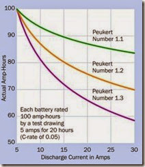
Figure 2-12 shows the probable actual performance of batteries with Peukert numbers of 1.1, 1.2, and 1.3. The curves were derived from the revised version of Peukert’s formula and show how the number of amp-hours that you can ex­ pect diminishes for each battery as the current increases. For example, if a battery that the man­ ufacturer has assigned a Peukert number of 1.2 is rated at 100Ah using the modern 20-hour test, but we draw 30A from it, the battery can actually deliver only 70Ah.

clip_image026

Figure 2-12. Actual amp-hour performance that should be expected from three batteries of Peukert numbers 1.1, 1.2, and 1.3 when they discharge currents ranging from 5 to 30 amps, assuming that the manufacturer has rated each battery at 100Ah using the modern system, which usually entails a 20-hour test (a C-rate of 0.05).

One additional factor: For any rechargeable bat­ tery, the Peukert number gradually increases with age, as the battery deteriorates chemically.

Voltage

The rated voltage of a fully charged battery is known as the open circuit voltage (abbreviated OCV or Voc), defined as the potential that exists when no load is imposed between the terminals. Because the internal resistance of a volt meter (or a multimeter, when it is used to measure DC volts) is very high, it can be connected directly between the battery terminals with no other load present, and will show the OCV quite accurately, without risk of damage to the meter. A fully charged 12-volt car battery may have an OCV of about 12.6 volts, while a fresh 9-volt alkaline bat­ tery typically has an OCV of about 9.5 volts. Be extremely careful to set a multimeter to measure DC volts before connecting it across the battery. Usually this entails plugging the wire from the red probe into a socket separately reserved for measuring voltage, not amperage.

The voltage delivered by a battery will be pulled down significantly when a load is applied to it, and will decrease further as time passes during a discharge cycle. For these reasons, a voltage regulator is required when a battery powers components such as digital integrated circuit chips, which do not tolerate a wide variation in voltage.

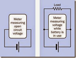
To measure voltage while a load is applied to the battery, the meter must be connected in parallel with the load. See Figure 2-13. This type of meas­ urement will give a reasonably accurate reading for the potential applied to the load, so long as the resistance of the load is relatively low com­ pared with the internal resistance of the meter.

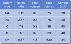
Figure 2-14 shows the performance of five com­ monly used sizes of alkaline batteries. The ratings in this chart were derived for alkaline batteries under favorable conditions, passing a small cur­ rent through a relatively high-ohm load for long periods (40 to 400 hours, depending on battery type). The test continued until the final voltage for each 1.5V battery was 0.8V, and the final volt­ age for the 9V battery was a mere 4.8V. These voltages were considered acceptable when the

clip_image028

Figure 2-13. When using a volt meter (or a multimeter configured to measure voltage), the meter can be applied directly between the battery terminals to determine the open-circuit voltage (OCV), or in parallel with a load to de- termine the voltage actually supplied during use. A multi- meter must be set to measure DC volts before connecting it across a battery. Any other setting may damage the me- ter.

Ah ratings for the batteries were calculated by the manufacturer, but in real-world situations, a final voltage of 4.8V from a 9V battery is likely to be unacceptable in many electronics applica­ tions.

clip_image030

Figure 2-14. The voltage delivered by a battery may drop to a low level while a manufacturer is establishing an amp- hour rating. Values for current, shown in the chart, were calculated subsequently as estimated averages, and should be considered approximate. (Derived from a chart published by Panasonic.)

As a general rule of thumb, if an application does not tolerate a significant voltage drop, the man­ ufacturer’s amp-hour rating for a small battery may be divided by 2 to obtain a realistic number.

How to Use it

When choosing a battery to power a circuit, considerations will include the intended shelf life, maximum and typical current drain, and battery weight. The amp-hour rating of a battery can be used as a very approximate guide to determine its suitability. For 5V circuits that impose a drain of 100mA or less, it is common to use a 9V battery, or six 1.5V batteries in series, passing current through a voltage regulator such as the LM7805. Note that the voltage regulator requires energy to function, and thus it imposes a voltage drop that will be dissipated as heat. The mini­ mum drop will vary depending on the type of regulator used.

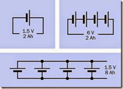
Batteries or cells may be used in series or in parallel. In series, the total voltage of the chain of cells is found by summing their individual voltages, while their amp-hour rating remains the same as for a single cell, assuming that all the cells are identical. Wired in parallel, the total voltage of the cells remains the same as for a single cell, while the combined amp-hour value is found by summing their individual amp-hour ratings, as­ suming that all the batteries are identical. See Figure 2-15.

In addition to their obvious advantage of portability, batteries have an additional advantage of being generally free from power spikes and noise that can cause sensitive components to misbe­ have. Consequently, the need for smoothing will depend only on possible noise created by other components in the circuit.

Motors or other inductive loads draw an initial surge that can be many times the current that they use after they start running. A battery must be chosen that will tolerate this surge without damage.

clip_image032

Figure 2-15. Theoretical results of using 1.5V cells in ser- ies or in parallel, assuming a 2Ah rating for one cell.

Because of the risk of fire, United States airline regulations limit the amp-hour capacity of lithium-ion batteries in any electronic device in carry-on or checked passenger baggage. If a de­ vice may be carried frequently as passenger bag­ gage (for example, emergency medical equip­ ment), NiMH batteries are preferred.

What Can Go Wrong
Short Circuits: Overheating and Fire

A battery capable of delivering significant cur­ rent can overheat, catch fire, or even explode if it is short-circuited. Dropping a wrench across the terminals of a car battery will result in a bright flash, a loud noise, and some molten metal. Even a 1.5-volt alkaline AA battery can become too hot to touch if its terminals are shorted together. (Never try this with a rechargeable battery, which has a much lower internal resistance, allowing much higher flow of current.) Lithium-ion bat­ teries are particularly dangerous, and almost al­ ways are packaged with a current-limiting com­ ponent that should not be disabled. A short- circuited lithium battery can explode.

If a battery pack is used as a cheap and simple workbench DC power supply, a fuse or circuit breaker should be included. Any device that uses significant battery power should be fused.

Diminished Performance Caused by Improper Recharging

Many types of batteries require a precisely meas­ ured charging voltage and a cycle that ends au­ tomatically when the battery is fully charged. Failure to observe this protocol can result in chemical damage that may not be reversible. A charger should be used that is specifically in­ tended for the type of battery. A detailed com­ parison of chargers and batteries is outside the scope of this encyclopedia.

Complete Discharge of Lead-Acid Battery

Complete or near-complete discharge of a lead- acid battery will significantly shorten its life (un­ less it is specifically designed for deep-cycle use

—although even then, more than an 80% dis­ charge is not generally recommended).

Inadequate Current

Chemical reactions inside a battery occur more slowly at low temperatures. Consequently, a cold battery cannot deliver as much current as a warm battery. For this reason, in winter weather, a car battery is less able to deliver high current. At the same time, because engine oil becomes more viscous as the temperature falls, the starter mo­ tor will demand more current to turn the engine. This combination of factors explains the tenden­ cy of car batteries to fail on cold winter mornings.

Incorrect Polarity

If a battery charger or generator is connected with a battery with incorrect polarity, the battery may experience permanent damage. The fuse or circuit breaker in a charger may prevent this from occurring and may also prevent damage to the charger, but this cannot be guaranteed.

If two high-capacity batteries are connected with opposite polarity (as may happen when a clumsy attempt is made to start a stalled car with jumper cables), the results may be explosive. Never lean over a car battery when attaching cables to it, and ideally, wear eye protection.

power > source > battery

Reverse Charging

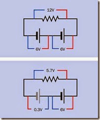
Reverse charging can occur when a battery be­ comes completely discharged while it is wired (correctly) in series with other batteries that are still delivering current. In the upper section of the schematic at Figure 2-16 two healthy 6V batter­ ies, in series, are powering a resistive load. The battery on the left applies a potential of 6 volts to the battery on the right, which adds its own 6 volts to create a full 12 volts across the load. The red and blue lines indicate volt meter leads, and the numbers show the reading that should be observed on the meter.

In the second schematic, the battery on the left has become exhausted and is now a “dead weight” in the circuit, indicated by its gray color. The battery on the right still sustains a 6-volt po­ tential. If the internal resistance of the dead bat­ tery is approximately 1 ohm and the resistance of the load is approximately 20 ohms, the poten­ tial across the dead battery will be about 0.3 volts, in the opposite direction to its normal charged voltage. Reverse charging will result and can damage the battery. To avoid this problem, a battery pack containing multiple cells should never be fully discharged.

Sulfurization

When a lead-acid battery is partially or com­ pletely discharged and is allowed to remain in that state, sulfur tends to build up on its metal plates. The sulfur gradually tends to harden, forming a barrier against the electrochemical re­ actions that are necessary to recharge the bat­ tery. For this reason, lead-acid batteries should not be allowed to sit for long periods in a dis­ charged condition. Anecdotal evidence sug­ gests that even a very small trickle-charging cur­ rent can prevent sulfurization, which is why some people recommend attaching a small solar panel to a battery that is seldom used—for example, on a sail boat, where the sole function of the bat­ tery is to start an auxiliary engine when there is insufficient wind.

clip_image034

Figure 2-16. When a pair of 6V batteries is placed in ser- ies to power a resistive load, if one of the batteries dis- charges completely, it becomes a load instead of a power source, and will be subjected to reverse charging, which may cause permanent damage.

High Current Flow Between Parallel Batteries
If two batteries are connected in parallel, with correct polarity, but one of them is fully charged while the other is not, the charged battery will attempt to recharge its neighbor. Because the batteries are wired directly together, the current will be limited only by their internal resistance and the resistance of the cables connecting them. This may lead to overheating and possible damage. The risk becomes more significant when linking batteries that have high Ah ratings. Ideally they should be protected from one an­ other by high-current fuses.
 

jumper What It Does , How It Works , Variants ,Values ,How to Use it and What Can Go Wrong

jumper

A jumper may also be referred to as a jumper socket or a shunt. A jumper should not be confused with jumper wires, which are not considered components for the purposes of this encyclopedia.

OTHER RELATED COMPONENTS

What It Does

A jumper is a low-cost substitute for a switch, where a connection has to be made (or unmade) only a few times during the lifetime of a product. Typically it allows a function or feature on a circuit board to be set on a semipermanent basis, often at the time of manufacture. A DIP switch performs the same function more conveniently. See “DIP” (page 43).

There is no standardized schematic symbol to represent a jumper.

How It Works

A jumper is a very small rectangular plastic tab containing two (or sometimes more) metal sock ets usually spaced either 0.1” or 2mm apart. The sockets are connected electrically inside the tab, so that when they are pushed over two (or more) pins that have been installed on a circuit board for this purpose, the jumper shorts the pins to­ gether. The pins are usually 0.025” square and are often part of a header that is soldered into the board. In a parts catalogue, jumpers may be found in a section titled “Headers and Wire Housings” or similar.

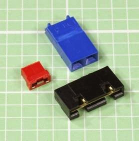
Three jumpers are shown in Figure 3-1. The blue one contains two sockets spaced 0.1” and is deep

enough to enclose the pins completely. The red one contains two sockets spaced 2mm and may allow the tips of the pins to emerge from its op­ posite end. The black one contains four sockets, each pair spaced 0.1” apart.

clip_image007

Figure 3-1. Three jumpers containing two sockets spaced 2mm (left), two sockets spaced 0.1” (top right), and four sockets, each pair spaced 0.1” (bottom right).


Variants


The set of pins with which a jumper is used is often referred to as a header. Headers are avail­ able with pins in single or dual rows. Some head­ ers are designed to be snapped off to provide the desired number of pins. A dual 28-pin header is shown in Figure 3-2 with a black jumper pushed onto a pair of pins near the midpoint.

clip_image009

Figure 3-2. A jumper pushed onto a pair of pins midway along a dual 28-pin header.

clip_image010

Variants

A jumper assembly may be a kit containing not only the jumper but also the array of pins with which it is intended to be used. Check the man­ ufacturer’s datasheet to find out exactly what is included.

The most common types of jumpers have two sockets only, but variants are available with as many as 12 sockets, which may be arranged in one or two rows. Header sockets may be used as a substitute for purpose-made jumpers, with the advantage that they are often sold in long strips that can be snapped off to provide as many sock­ ets as needed. However, the pins attached to header sockets must be manually connected by soldering small lengths of wire between them.

In some jumpers, the plastic tab extends upward for about half an inch and functions as a finger grip, making the jumper much easier to hold during insertion and removal. This is a desirable feature if there is room to accommodate it.

The sockets inside a jumper are often made from phosphor-bronze, copper-nickel alloy, tin alloy, or brass alloy. They are usually gold-plated, but in some instances are tin-plated.

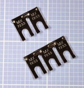
Rarely, a jumper may consist of a metal strip with U-shaped connections suitable for being used in conjunction with screw terminals. Two jumpers of this type are shown in Figure 3-3. They should not be confused with high-amperage fuses that look superficially similar.

clip_image012

Figure 3-3. These jumpers are designed to short together two or three screw terminals.

Values

The spacing between the sockets in a jumper is referred to as its pitch. As previously noted, 0.1” and 2mm are the most popular values.

A typical maximum rating for a jumper of 0.1” pitch is 2A or 2.5A at 250V.

18 Encyclopedia of Electronic Components Volume 1

How to Use it

A jumper may activate a “set it and forget it” cir­ cuit function. An example would be the factory configuration of a product to work with 115VAC or 230VAC power input. End users were expected to set jumpers in some computer equipment sold during the 1980s, but this is no longer the case.

What Can Go Wrong

Jumpers are easily dropped, easily lost, and easily placed incorrectly. When purchasing jumpers, buy extras to compensate for their fragility and the ease of losing them.

Any location where a jumper may be used should be clearly labelled to define the function of each setting.

Cheap, poorly made jumpers may self-destruct from mechanical stresses when removed from their pins. The plastic casing can come away, leaving the sockets clinging naked to the pins protruding from the circuit board. This is another reason why it is a good idea to have a small stock of spare jumpers for emergencies.

Oxidation in jumpers where the contacts are not gold- or silver-plated can create electrical resist­ance or unreliable connections.


8015 Serial Data Communication ,8051 Data Communication Modes and Summary of 8015 Serial Data Communication

8051 Data Communication Modes

The 8051 has one serial port-port pins 3.0 (RXD) and 3.1 (TXD)-that receives and transmits data. All data is transmitted or received in two registers with one name: SBUF. Writing to SBUF results in data transmission; reading SBUF accesses received data. Transmission and reception can take place simultaneously, and the receiver can be in the process of receiving a byte while a previous byte is still in SBUF. The first byte must be read before the reception is complete, or the second byte will be lost.

Physically the data is a series of voltage levels that are sampled, in the center of the bit period, at a frequency that is determined by the serial data mode and the program that controls that mode. All devices that wish to communicate must use the same voltage levels, mode, character code, and sampling frequency (baud rate). The wires that connect the ports must also have the same polarity so that the idle state, logic high, is seen by all ports.

The installation and checkout of a large distributed system are subject to violations of all of the "same" constraints listed previously. Careful planning is essential if cost and time overruns are to be avoided.

The four communication modes possible with the 8051 present the system designer and programmer with opportunities to conduct very sophisticated data communication networks.

Mode 0:Shift Register Mode

Mode 0 is not suitable for the interchange of data between 8051 microcontrollers. Mode 0 uses SBUF as an 8-bit shift register that transmits and receives data on port pin 3.0, while using pin 3.1 to output the shift clock. The data and the shift clock are synchronized using the six internal machine states, and even for microcontrollers using the same crystal fre­quency, they can be slightly out of phase due to differences in reset and start-up times.

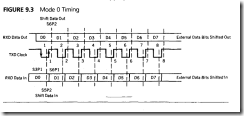
Figure 9.3 shows the timing for the transmission and reception of a data character.

Remember that the shift clock is generated internally and is always from the 8051 to the external shift register. The clock runs at the machine cycle frequency of fl l 2. Note that transmission is enabled any time SBUF is the destination of a write operation, regardless of the state of the transmitter empty flag, SCON bit l (T1).

clip_image002

Data is transmitted, LSB first, when the program writes to SBUF. Data is shifted right during S6P2, or 24/f seconds after the rising edge of the shift clock at S6PI. Data is stable from just after S6P2 for one cycle. Good design practice dictates that the data be shifted into the external shift register during the high-to-low transition of the shift clock, at S3Pl, to avoid problems with clock skew.

The receiver is enabled when SCON bit 5 (REN) is enabled by software and SCON bit 0 (RI) is set to 0. At the end of reception RI will set, inhibiting any form of character reception until reset by the software. The condition of RI cleared to 0 is unique for mode 0; all other modes are enabled to receive when REN is set without regard as to the state of RI. The reason is clear: Mode 0 is the only mode that controls when reception can take place. Enabling reception also enables the clock pulses that shift the received data into the receiver.

Reception begins, LSB first, with the data that is present during S5P2, or 24/f sec­onds before the rising edge of the shift clock at S6Pl. The incoming data is shifted to the right. Incoming data should be stable during the low state of the shift clock, and good design practice indicates that the data be shifted from the external shift register during the low-to-high transition of the shift clock, at S6Pl, so that the data is stable up to one clock period before it is sampled.

A serial data transmission interrupt is generated at the end of the transmission or re­ception of bit eight if enabled by the ES interrupt bit El.4 of the enable interrupt register. Software must reset the interrupting bit RI or T1. As the same physical pin is used for transmission and reception, simultaneous interrupts are not possible.
Mode 0 is well suited for rapid data collection and control of multi-point systems that use a simple two-wire system for data interchange. Multiple external shift registers can expand the external points to an almost infinite number. limited only by the response time desired for the application. For instance, at f = 16 megahertz, each point of a 10,000 point system could be monitored every 60 milliseconds. Common industrial systems do not require rates this high, and a reasonable rate of one point per second would leave adequate time for processing by the program.

Mode zero

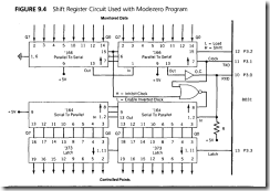
A small system that features 16 points of monitored data and 16 points of control is shown in Figure 9.4. Data from the process is converted from parallel to serial in the’ 166 type registers. Data to the process is converted from serial to parallel in the type ‘164 registers and latched into the ·373 latches.

It is important that the data be "frozen" before the shifting begins. The bits shifted in could be changed before reaching the microcontroller, or a control hit might be changed, momentarily, as it shifts through the output shift registers. Port pin 3.2 is used to disable the input registers from the process when high and to enable loading input values when low.

To read the inputs, P3.2 is brought high and the receiver is enabled (twice) to generate 16 input shift clocks. The high level on P3.2 prevents the shift clocks from reaching the output registers. At the end of the read, P3.2 is brought low to enable loading input values into the input registers. No clock pulses are generated, so the output control registers do not change state.

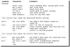
Control bits to the output registers are transmitted when P3.2 is low and SBUF has two data bytes written in succession. The two bytes generate 16 clock pulses that fill the output registers with the SBUF data. Port pin 3.3 is used to latch the newly shifted control data to the process by strobing the output data latches. A program that monitors and con­trols the points follows.

clip_image004

The program "mode zero" monitors 16 bits and controls the state of 16 bits. The system can be expanded indefinitely by expanding the shift register configurations shown in Figure 9.4. In this example program, whatever data is read on the monitored points is written to the control points. The direction of data flow to/from the 8051 is controlled by P3.2, (high = in). P3.3 latches new data to the process.

clip_image006

clip_image008

COMMENT

Note that in both the transmit and receive cases the interrupt bit must go high before the subroutine can be ended.

The data transmit and reception time is so short that interrupt-driven schemes are not efficient.

Mode 1: Standard 8-Bit UART Mode

In Chapter 7, several simple communication programs are studied that use the serial port configured as mode I, the standard UART mode normally used to communicate in 8-bit ASCII code. Only seven bits are needed to encode the entire set of ASCII characters. The eighth bit can be used for even or odd parity or ignored completely. Asynchronous data transmission requires a start and stop bit to enable the receiving circuitry to detect the start and finish of a complete character. A total of ten bits is needed to transmit the 7-bit ASCII character, as shown in Figure 9.5.

Transmission begins whenever data is written to SBUF. It is the responsibility of the programmer to ensure that any previous character has been transmitted by inspecting the TI bit in SCON for a set condition. Data transmission begins with a high-to-low start bit transition on TXD that signals receiving circuitry that a new character is about to arrive. The 8-bit character follows, LSB first and MSB parity bit last, and then the stop bit, which is high for one bit period. If another character follows immediately, a new start bit is signaled by a high-to-low transition; otherwise, the line remains high. The width of each transmitted data bit is controlled by the baud rate clock used. The receiver must use the same baud rate as the transmitter, or it reads the data at the wrong time in the character stream.

clip_image010

Reception begins if the REN bit is set in SCON and a high-to-low transition is sensed on RXD. Data bits are sampled at the baud rate in the center of the bit duration period. The received character is loaded into SBUF and the stop bit into SCON bit 2 (RBS) if the RI bit in SCON is cleared, indicating that the program has read the previous character; and either SM2 in SCON is cleared or SM2 is set and the received stop bit is high, which is the normal state for stop bits.

If these conditions are met, then SBUF is loaded with the received character, and RI is set. If the conditions are not met, the character is ignored, RI is not set, and the receive circuitry awaits the next start bit.

The restriction that a new character is not accepted unless RI is cleared seems reason­able. Data is lost if either the previous byte is overwritten or the new byte discarded, which is the action taken by the S05 l. The restriction on SM2 and the stop bit are not as obvious. Normally, SM2 will be set to 0, and the character will be accepted no matter what the state of the stop bit. Software can check RBS to ensure that the stop bit is correct before accepting the character if that is thought to be important.

Possible reasons for setting SM2 to force reception only when the stop bit is a I could be useful if the transmitter has the ability to change the stop bit from the normal high state. If the transmitter has this capability, then the stop bit can serve as an address bit in a multiprocessor environment where many loop microcontrollers are all receiving the same transmission. Only the microcontroller that has SM2 cleared can receive characters end­ing in either of the stop bit states. If all the microcontrollers but one have SM2 set, then all data transmissions ending in a low stop bit interrupt the unit with SM2 = O; the rest ignore the data. Transmissions ending in a high stop bit can interrupt all microcontrollers.

Transmitters with the capability to alter the stop bit state are not standard. The 8051 communication modes 2 and 3 use the SM2 bit for multiprocessing. Mode 1 is not needed for this use.

In summary, mode 1 should be used with SM2 cleared, as a standard S-bit UART, with software checks for proper stop bit magnitude if needed. As discussed in Chapter 7, the baud rate for modes 1 and 3 are determined by the overflow rate of timer 1, which is usually configured as an auto-reload timer. PCON bit 7 (SMOD) can double the baud rate when set.

Modeone

Mode 1 is most likely to be used in a dedicated system where the S05 I serial port is con­nected to a single similar port. A program that transmits and receives large blocks of data on an interrupt-driven basis is developed to investigate some problems common to data inter­change programs.

To the main program, interrupt-driven communication routines are transparent: Data appears in RAM as it is received and disappears from RAM as it is transmitted. In both cases, the link between the main program and the interrupt-driven communication sub-routines are areas of RAM called buffers. These buffers serve to store messages that are to be sent and messages that are received.

Each buffer area is defined by two memory pointers. One pointer contains the address of the top of the huff er, or the location in RAM where the next character is to be stored, and the second contains the address of the next character to be read. The buffers are named "inbuf," for use in storing characters as they are received, and "outbuf’," for stor­ing characters that are to be sent. The pointers to the tops of the buffers are named "intop" and "outop." respectively, while the pointers to the next character to be read are named "inplace " and "outplace."

The two buffers work in exactly the same way. The receive subroutine fills inbuf as characters are received and updates intop as it operates. The main program empties inbuf as it can and keeps inplace pointing to the next character to be read. The main program fills outbuf, while keeping outop updated to point to the next character to be stored. The transmission subroutine empties outbuf as it can and keeps outplace pointing to the next character to be read from outbuf,

These actions continue until the pointer to the top of the buffer equals the pointer to the next character. The buffer is now empty. and the pointers can be reset to the bottom of the buffer.

The buffer areas and pointers may be summarized as follows:

Outbuf: An area of RAM that holds characters to be transmitted

Outop: Pointer to outbuf that holds the address of the next character to be stored by the main program for transmission

Outplace: Pointer to outbuf that holds the address of the next character to he trans­mitted by the transmit subroutine

lnbuf: An area of RAM that holds received characters

Intop: Pointer to inbuf that holds the address of the next character received by the receive subroutine

lnplace: Pointer to inbuf that holds the address of the next character to be read by the main program

The main program and the transmit subroutine does not read data from a buffer when­ever the place pointer equals the top pointer, which indicates that the buffer is empty.

The programmer has to make an estimate of how large the buffers need to be. Some­times the general nature of the data is known when the system is in the design phase. The programmer(s) for the two computers that are communicating can define message length and frequency, arriving at a worst-case buffer size.

If the 8051 is part of a peripheral, such as a printer, that randomly receives large quantities of data, then the buffer size is fixed at an economic and competitive number using external RAM. For short and infrequent messages, internal RAM may suffice. In both cases, the receiving subroutine should have a means of communicating to the source of data when inbuf is becoming full so that the data flow can be suspended while inhuf is emptied. Our example program falls somewhere between these extremes; some external RAM will be needed, but not 32 kilobytes.

Registers RO and RI of register banks 0 and I are used effectively as pointers to the first 256d bytes of external RAM using MOVX instructions. For this example, the buffer sizes are fixed at I 28d bytes each, although there is no need for them to be of equal size. Larger buffers can be constructed using the DPTR.

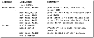
A program named "Modeone" handles communications between the 8051 and another computer using serial data mode I. Two I 28d byte buffers in external RAM store charac-ters to be transmitted or received. R0and R1 of register bank 0 keep track of data flow for the receive buffer inbuf, located in external RAM addresses 00h to 7Fh. R0and RI of register bank I serve the transmit buffer outbuf, external RAM addresses 80h to FFh. R0 is the place pointer, RI the top pointer to the buffers. The baud rate is set by timer I in the auto-reload mode to 1200 bits per second. Port pin 3.2 is set high when inbuf is I byte from a full condition.

clip_image012

clip_image014

cOMMENT

Note that the program has to initiate the first interrupt for the first character that is stored in a previously empty outbuf. If the first interrupt action were not done, transmission would never take place, as the T1 bit would remain a 0. The 0 state of the Tl bit is ambiguous: It can mean that the transmitter is busy sending a byte or that no activity is taking place at all. The 1 state of T1 is specific: A byte has been transmitted, and SBUF can receive the next byte.

The example program fills outbuf quickly, until outop rolls over to 00h. Outbuf is emptied until outplace rolls over also, and outbuf is re-initialized to BOh. Received data is always read before inbuf can fill up, as there is very little for the program to do. Adding a time delay in the program ensures that inbuf grows beyond one byte.

COMMENT

The data source should cease sending data to the 8051 until port 3.2 goes low. In this example, "full" is arbitrarily set at one byte below the maximum capacity of inbuf. The actual number for a full condition should be set at maximum capacity less the response time of the source expressed in characters.

No feedback from the source to the 8051 has been provided for halting transmission of data from the 8051. Feedback can be accomplished by using one of the INT lines as an input from the source to signal a full condition.

Modes 2 and 3: Multiprocessor

Modes 2 and 3 are identical except for the baud rate. Mode 2 uses a baud rate of f/32 if SMOD (PCON. 7) is cleared or f/64 if SMOD is set. For our 16 megahertz example, this results in baud rates of 500000 and 250000 bits per second, respectively. Pulse rates of these frequencies require care in the selection and installation of the transmission lines used to carry the data.

Baud rates for mode 3 are programmable using the overflows of timer I exactly as for data mode I. Baud rates as high as S3333 bits per second are possible using a 16 mega­hertz crystal. These rates are compatible with RS 485 twisted-pair transmission lines.

Data transmission using modes 2 and 3 features eleven bits per character, as shown in Figure 9.6. A character begins with a start bit, which is a high-to-low transition that lasts one bit period, followed by S data bits, LSB first. The tenth bit of this character is a pro­grammable bit that is followed by a stop bit. The stop bit remains in a high state for a minimum of one bit period.

Inspection of Figures 9.5 and 9.6 reveals that the only difference between mode l and mode 2 and 3 data transmission is the addition of the programmable tenth bit in mode 2 and 3.

When the S05 l transmits a character in mode 2 and 3, the eight data bits are whatever value is loaded in SBUF. The tenth bit is the value of bit SCON.3, named TDS. This bit can be cleared or set by the program. Interrupt bit T1 (SCON. I) is set after a character has been transmitted and must be reset by program action.

Characters received using mode 2 and 3 have the eight data bits placed in SBUF and the tenth bit is in SCON.2, called RBS, if certain conditions are true. Two conditions apply to receive a character. First, interrupt bit RI (SCON.O) must be cleared before the last bit of the character is received, and second, bit SM2 (SCON.5) must be a 0 or the tenth bit must be a I. If these conditions are met, then the eight data bits are loaded in SBUF, the tenth bit is placed in RBS, and the receive interrupt bit RI is set. If these con­ditions are not met, the character is ignored, and the receiving circuitry awaits the next start bit.

The significant condition is the second. If RI is set, then the software has not read the previous data (or forgot to reset RI), and it would serve no purpose to overwrite the

clip_image016

data. Clearing SM2 to 0 allows the reception of multiprocessor characters transmitted in mode 2 and 3. Setting SM2 to 1 prevents the reception of those characters that have bit ten equal to 0. Put another way, if bit ten is a 1, then reception always takes place; SM2 is ignored. If bit ten is a 0 then only those receivers with SM2 set to 0 are interrupted.

Mode 2 and 3 has been included in the 8051 specifically to enhance the use of mul­tiple 8051 s that are connected to a common loop in a multiprocessor configuration. The term multiprocessing implies many processors acting in some unified manner and con­nected so that data can be interchanged between them. When the processors are connected in a loop configuration. then there is generally a controlling or "talker" processor that directs the activities of the remainder of the loop units. or "listeners."

One particular characteristic of a talker-listener loop is the frequent transmission of data between the talker and individual listeners. All data broadcast by the talker is received by all the listeners, although often the data is intended only for one or a few listeners. At times, data is broadcast that is meant to be used by all the listeners.

There are many ways to handle the addressing problem. Systems that use standard UART technology, such as mode I, can assign unique addresses to all the listeners. Each message from the talker can begin with the address of the particular listener for which it is intended. When a message is sent, all the listeners process the message and react only if the address that begins the message matches their assigned addresses. If messages are sent frequently, the listeners will waste a lot of processing time rejecting those messages not addressed to them.

Mode 2 and 3 reduces processing time by enabling character reception based upon the state of SM2 in a listener and the state of bit ten in the transmitted character. A single strategy is used to enable a few listeners to receive data while the majority ignore the transmissions.

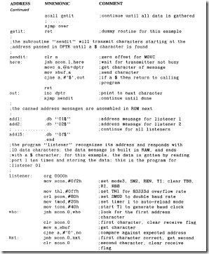
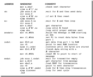
All listeners initially have SM2 set to 0, the normal reset state, and receive all multi­processor messages. Each listener has a unique address. The talker addresses each of the listeners that are not of interest and commands them to set SM2 to I, leaving the listeners to which communication is desired with SM2 cleared to 0. All characters from the talker to the unique listeners are then sent with bit ten set to 0. The listener(s) with SM2 cleared receive the data; those with SM2 set ignore the data due to the condition of bit ten. Com­munication with all listeners is done by setting bit ten to 1. which enables reception of characters with no regard as to the state of SM2.

A variation of this strategy is to have all listeners set SM2 to I upon power-up. All address messages have a I in bit position ten, so all listeners receive and process any address message to see whether action is required. Listeners chosen are commanded in the address message to set SM2 to 0, and data communication proceeds with bit ten cleared to 0.

The multiprocessing strategy works best when there is extensive data interchange between the talker and each individual listener. Frequent changes of listeners with little data flow results in heavy address usage and subsequent interruption of all listeners to process the address messages.

Modethree

A multiprocessor configuration that demonstrates the use of mode 3 is shown in Figure 9.7. An RS 485 twisted-pair transmission line is used to form a loop that has 15d 8051 microprocessors connected to the lines so that all data on the loop is common to all serial ports. The 8051 has been programmed to be the talker, and the rest are listeners.

The purpose of the loop is to collect ten data bytes from each listener, in sequential order. All listeners initialize SM2 to I after power-up. and the talker configures all address

clip_image018

messages using a 1 in bit ten. Addressed listeners transmit ten data characters to the talker with bit ten set to 0. The talker has SM2 set to 0 so that all communications from listeners are acknowledged. Data characters from a listener to the talker are ignored by the remain­ing listeners. At the end of the ten data bytes, the addressed listener resets SM2 to 1. The data rate is set by timer 1 in the auto-reload mode to be 83333 baud. That portion of the talker and listener program that has to do with setting up the multiprocessor environment will be programmed.

The messages that are sent from the talker to the listeners are called "canned" because the contents of each is known when the program is written; the messages can be placed in ROM for later use. The subroutine "sendit" in the talker program can send canned mes­sages of arbitrary length, as long as each message ends in the character$.

Message contents from the listeners to the talker are not known when the program is written. A version of sendit, "sndat," can still be used if the message is constructed in the same manner as the canned messages in the ROM of the talker program.

The program "Modethree " sends a canned address message to each of Fh listeners on a party-line loop using serial data mode 3. All canned messages are transmitted with bit ten set to I; all received data from the addressed listener has bit ten set to 0. SM2 is set in all listeners and reset in the talker.

clip_image020

clip_image022

clip_image024

COMMENT

The inclusion of the $ character in each message is useful both as a check for the end of a message and to reset a listener that somehow misses one of the three characters expected in an address. If a listener misses a character, due to noise for example, it will get to the "no" label within one or two characters. The next $ will reset the listener program back to the "who" label.

Programs that interchange data must be written to eliminate any chance of a receiving unit getting caught in a trap waiting for a predetermined number of characters. Common schemes that accomplish this goal use special "end-ot-messsqe" characters, as in the case of Mode three, or set timers to interrupt the receiving program if the data is not received within a certain period of time.

Much more elaborate protocols than those used here in this example would be used by the listeners when sending data to the talker. There is always the possibility that errors will occur due to noise or the improper operation of another listener interfering. The talker may store these errors. Error-checking bytes may be added to the data stream so that the talker can verify that the string of characters is error free.

Summary of 8015 Serial Data Communication

Four serial data communication modes for the 8051 are covered in this chapter:

Mode 0: High-speed, 8-bit shift register; one baud rate off/ 12

Mode 1: Standard 8-bit UART; variable baud rate using timer 1 overflows

Mode 2: Multiprocessor 9-bit UART: two baud rates of f/32 and f/64

Mode 3: Multiprocessor 9-bit UART: variable baud rate using timer 1over flows

Programs in this chapter use these modes and feature several standard communication techniques:

High-speed shift register data gathering

Interrupt-driven transmit and receive buffers

Sending preprogrammed, or canned, messages

Problems

I. Explain why mode 0 is not suitable for 8051 communications.

2. How much clock skew. in terms of clock period, can transmitted data using mode 0 have before data is shifted in error?

3. Repeat Problem 2 for data reception.

4. Assume you are determined to use mode 0 as a communication mode from one 8051 to another. Outline a system of hardware and software that would allow this. Hint: A "buffer" is needed.

5. Sketch the mode I no parity ASC11 serial characters U. 0. and w.

6. Many communication terminals can determine the baud rate of standard (mode 1) char· acrers by making measurements on the first few "fill" characters received. Outline a program strategy that would set the 8051 baud rate automatically based upon the first character received.

7. Character transmission can be done by using a time delay greater than the character time before moving a new byte to SBUF. Explain why character reception must use an inter­rupt flag if all characters are to be received.

8. ASCII characters can have even (number of ones). odd, or no parity using bit 7 as a parity bit. Write a program that checks the incoming data for odd parity and sets a flag if the parity is incorrect.

9. Write a program that converts odd parity bytes to even parity bytes (bit 7 is the parity bit).

10. An overrun is said to occur in data reception whenever a new byte of data is received before the previously received byte has been read. Discuss two methods by which over­runs might be detected by the 8051 program.

11. List two reasons why stop bits arc used in asynchronous communications.

12. A framing error is said to have occurred if the stop bit is not a logic high. What mode(s) can detect a framing error?

13. Why is it necessary for the main program (see "Modeone") to set the T1 bit to begin the transmission of a string of characters using interrupt-driven routines? Name another way for the main program to initiate transmission.

14. Determine if an 8051 in mode I can communicate with an 8051 in mode 3.

15. Modify the "Modeone " program to use 4K byte buffers.


8015 Serial Data Communication ,Introduction and Network Configurations

Introduction

Chapter 2 contained an extensive review of serial data communication concepts and the hardware and software that is built into the 8051 for enabling serial data transfers. Chapter 7 contained some brief programming examples of how this capability may be used. Serial data transmission has become so important to the overall computing strategy of industrial and commercial applications that a separate chapter on this crucial subject is appropriate.

One hallmark of contemporary computer systems is interconnectivity: the joining of computers via data networks that link the computers to each other and to shared resources, such as disk drives, printers, and other I/O devices. The beginning of the "computer age" saw isolated CPUs connected to their peripherals using manufacturer-specific data trans­mission configurations. One of the peripherals, however, was the teletype that had been borrowed from the telephone industry for use as a human interface to the computer, using the built-in keyboard and printer.

The teletype was designed to communicate using standard voice grade telephone lines via a modem (Modulator demodulator) that converts digital signals to analog frequencies and analog frequencies to digital signals. The data, by the very nature of telephone voice transmission, is sent and received serially. Various computer manufacturers adapted their equipment to fit the teletype, and, perhaps, the first "standard" interface in the industry was born.

This standard was enhanced in the early I 960’s with the establishment of an electrical/ mechanical specification for serial darn transmission that was assigned the number RS 232

by the Electronics Industry Association. A standard data code was also defined for all the characters in the alphahet, decimal numbers. punctuation marks. and control characters. Based on earlier telephonic codes. the standard hecame known as the American Standard Code for Information Interchange (ASC11).

The establishment of RS 232 and ASC11 coincided with the development of multi­user computer organizations wherein a number of users were Jinked to a host mainframe via serial data Jinks. By now. the CRT terminal had replaced the slower teletype. but the RS 232 serial plug remained, and serial data was encoded in ASCII. Peripheral devices, such as printers. adopted the same standards in order to access the growing market for serial devices.

Serial data transmission using ASC11 became so universal that specialized integrated circuits, Universal Asynchronous Receiver Transmitters (UARTS) were developed to per­form the tasks of converting an 8-bit parallel data byte to a l0-bit serial stream and con­verting 10-bit serial data to an 8-bit parallel byte. When the second-generation 8051 microcontrollcr was designed. the UART became part of the circuit.

Chapter 7 introduced the basic programming concepts concerning transmitting and receiving data using the serial port of the 8051. In this chapter. we study the serial data modes available to the programmer and develop programs that use these modes. The four modes arc as follows:

Mode 0: Shift register mode

Mode I: Standard UART mode

Mode 2: Multiprocessor fixed mode

Mode 3: Multiprocessor variable mode

In this chapter, we also identify multiprocessor configurations that are appropriate for each mode and write sample programs to enable data communication between 8051 microcontrollers.

Network Configurations

The first problem faced by the network system designer is how to physically hook the computers together. The two possible basic configurations are the star and the loop, which arc shown in Figure 9. 1.

The star features one line from a central computer to each remote computer, or from "host" to "node." This configuration is often used in time-sharing applications when a central mainframe computer is connected to remote terminals or personal computers using a dedicated line for each node. Each node sees only the data on its line; all communication is private from host to node.

The loop uses one communication line to connect all of the computers together. There may he a single host that controls all actions on the loop, or any computer may be enabled to he the host at any given time. The loop configuration is often used in data-gathering applications where the host periodically interrogates each node to collect the latest infor­mation about the monitored process. All nodes see all data; the communication is public between host and nodes.

Choosing the configuration to use depends upon many external factors that are often beyond the control of the system designer. Some general guidelines for selection are shown in the following table:

FIGURE 9.1 Communication Configurations

clip_image002

Objective

Network

Comments

Reliability

Star

Single node loss per line loss

Fault isolation

Star

Fault traceable to node and line

Speed

Star

Each node has complete line use

Cost

Loop

Single line for all nodes

The star is a good choice when the number of nodes is small, or the physical distance from host to node is short. But, as the number of nodes grows, the cost and physical space represented by the cables from host to nodes begins to represent the major cost item in the system budget. The loop configuration becomes attractive as cost constraints begin to out­weigh other considerations.

Microcontrollers are usually applied in industrial systems in large numbers distributed over long distances. Loop networks are advantageous in these situations, often with a host controlling data transmission on the loop. Host software is used to expedite fault

FIGURE 9.2 Hybrid Communication Configurations

clip_image004

and, thus, improve system reliability. High speed data transmission schemes can be em­ployed to enhance system response time where necessary.

The old racing adage "Speed costs money: How fast do you want to go?" should be kept in mind when designing a loop system. Successors to RS 232, most notably RS 485, have given the system designer 100 kilobaud rates over 4000-foot distances using inexpen­sive twisted-pair transmission Jines. Faster data rates are possible at shorter distances, or more expensive transmission lines, such as coaxial cable, can be employed. Remember that wiring costs are often the major constraint in the design of large distributed systems.

Many hybrid network arrangements have evolved from the star and the loop. Fig­ure 9. 2 shows two of the more popular types that contain features found in both basic configurations.


8051 Applications (Pulse Measurement and Multiple Interrupts)

Pulse Measurement

Sensors used for industrial and commercial control applications frequenT1y produce pulses that contain information about the quantity sensed. Varying the sensor output frequency, using a constant duty cycle but variable frequency pulses to indicate changes in the mea­sured variable, is most common. Varying the duration of the pulse width, resulting in constant frequency but variable duty cycle, is also used. In this section, we examine programs that deal with both techniques.

Measuring Frequency

Timers TO and T 1 can be used to measure external frequencies by configuring one timer as a counter and using the second timer to generate a timing interval over which the first can count. The frequency of the counted pulse train is.then

Unknown frequency = Counter/timer

For example, if the counter counts 200 pulses over an interval of .1 second generated by the timer. the frequency is

UF = 200/. 1 = 2000 Hz

Certain fundamental limitations govern the range of frequencies that can be mea­sured. An input pulse must make a l-to-0 transition lasting two machine cycles. or f/24, to be counted. This restriction on pulse deviation yields a frequency of 667 kilohertz using our 16 megahertz crystal (assuming a square wave input).

The lowest frequency that can be counted is limited by the duration of the time inter­val generated, which can be exceedingly long using all the RAM to count timer rollovers (49.15 milliseconds x 2"32768). There is no practical limitation on the lowest frequency that can be counted.

Happily, most frequency variable sensors generate signals that fall inside of 0 to 667 kilohertz. Usually the signals have a range of 1,000 to io,000 hertz.

Our example will use a sensor that measures de voltage from 0 to 5 volts. At 0 V the sensor output is 1,000 hertz, and at full scale, or 5 volts, the sensor output is 6,000 hertz. The correspondence is I volt per 1,000 hertz, and we wish to be able to measure the volt­age to the nearest .OJ V, or io hertz of resolution (assuming the sensor is this accurate). A timing interval of I second generates a frequency count accurate to the nearest I hertz, so an interval of . I s yields a count accurate to the nearest 1 0 hertz.

Another way to arrive at the desired timing interval, T, is to note that the desired accuracy is

clip_image002

and that the range of the counter is from T x fmin to T x fmax, or a range of T x (fmax – fmin) from zero to full scale. The resolution of each counter bit is then

clip_image004

where n is the desired number of bits to be resolved. For our example, T = 512/5000 = . io24 seconds; . I second yields a slighT1y better accuracy.

From earlier tries at generating decimal time delays in Chapter 7. it has been amply demonstrated that these cannot be done perfecT1y using a 16 megahertz crystal (. 75 micro­second count interval). We will be close enough to meet our requirements.

T1 is used in the auto-reload mode 2 to generate overflow interrupts every I 92 microseconds (256 x . 75 microseconds). These overflows are counted using R4 and R5 until .io0032 seconds have elapsed (52Jd overflows). For this example, TO is used as a counter to count the external frequency that is fed to the port 3.4 (TO) pin during the T1 interval. Using the interval chosen, the range of counts in TO becomes

OV = io00 Hz x . io0032 s = io0d counts

5V = 6000 Hz x . 1 00032 s = 600d counts

.OJ V = ioHz x . io0032 s = 1 count

which meets the desired accuracy specification.

Freq

The program "freq" uses TO to count an external pulse train that is known to vary in frequency from io00 to 6000 hertz. T1 generates an exact time delay of 192 microseconds that is counted using registers R4 and R5 of bank I until T1 has overflowed 521d times, or a total delay of. io0032 seconds.

clip_image006

COMMENT

The longer the time taken to count, the more accurate the frequency will be (but remember, it makes litT1e sense to make the readout more accurate than the basic sensor). TO will overflow at 6S,535 or at the end of an interval of io.92 sat fmax, which can be generated in T1 and R4, RS. In this case, the accuracy would be to the nearest .09 hertz (.0001 volt).

If you wish to generate a delay closer to . 1 s than used in the example, make T1 cycle in a shorter period of time and count these shorter periods in R4, RS. Compensate for the 8.5 microseconds it takes for the interrupt routine to determine that time is up.

Preloading TO with a number that causes TO to overflow to 0000 when fmin is present during T will enable TO to read the voltage direcT1y. for our example, presetting TO to FF9Ch will have TO= 01F4h (500d) at fmax = 60,000 hertz for T = .1 s.

Pulse Width Measurement

Theoretically, if the input pulse is known to be a perfect square wave, the pulse frequency can be measured by finding the time the wave is high (Th). The frequency is then

clip_image008

If Th is 200 microseconds, for example, then UF is 2500 hertz. The accuracy of the mea­surement will fall as the input wave departs from a 50 percent duty cycle.

Timer X may be configured so that the internal clock is counted only when the corre­sponding I͞N͞T͞X pin is high by setting the GATE X bit in TMOD. The accuracy of the measurement is within approximately one-half of the timer clock period, or .375 micro­second for a 16 megahertz crystal. This accuracy can only be attained if the measurement is started when the input wave is low and stopped when the input next goes low. Pulse widths greater than the capacity of the counter, which is 49.152 milliseconds for a 16 megahertz crystal, can be measured by counting the overflows of the timer flag and adding the final contents in the counter.

For the example in this section, the sensor used to measure the 0 volt to 5 volts de voltage has a fixed frequency of io00 hertz or a period of I ms. For a 0 volt input, the sensor is high for 400 microseconds and low for 600 microseconds; when the sensor input is 5 volts, the output is high for 900 microseconds and low for io0 microseconds. Each volt represents io0 microseconds of time; the accuracy of the measurement is ❗ .00325 volts, which is within the specification of .OJ volt.

To make the measurement, TO will be configured to count the internal clock when I͞N͞T͞0 is high. The measurement is not started until I͞N͞T͞0 goes from high to low, leaving a minimum of I 00 microseconds to start TO. The measurement is made while I͞N͞T͞0 is high and stopped when I͞N͞T͞0 goes low again. The whole process can be interrupt driven by using the interrupt Hag associated with I͞N͞T͞0 . The IEO flag can be set whenever I͞N͞T͞0 goes from high to low to notify the program to start the pulse width timing and then to stop. A variation of this program is currenT1y in use to measure fabric width by measuring the reflection time of a scanning laser.

Width

The program "Width" measures the width of pulses that are fed to the I͞N͞T͞0 pin, port 3.2 and that are known to vary from 400 to 900 microseconds. The program starts when the interrupt Hag IEO is set and stops the next time the Hag is set, indicating one complete cycle of the input wave.

clip_image010

COMMENT

If there is a considerable amount of electrical noise present on the I͞N͞T͞0 pin, an average value of the pulse width could be found by measuring the widths of a number of consecutive pulses. A counter could be incremented at the end of each cycle and the sum of the widths divided by the counter contents. The noise should average to zero.

Frequency can be measured by timing the interval of a number (M) of high-to-low I͞N͞T͞X inter­rupts. Synchronize the timing by starting the timer at the first transition. and stop the timer at the Mth + 1 transition. The frequency is then

clip_image012

where T is the count in the timer.

D/ A and A/D Conversions

Conversion between the analog and digital worlds requires the use of integrated circuits that have been designed to interface with computers. Highly intelligent converters are commercially available that all have the following essential characteristics:

Parallel data bus: tri-state, 8-bit

Control bus: enable (chip select), read/write, ready/busy

The choice the designer must make is whether to use the converter as a RAM memory location connected to the memory busses or as an I/O device connected to the ports. Once that choice is made, the set of instructions available to the programmer becomes limited. The memory location assignment is the most restrictive, having only MOVX available. The design could use the additional 32K RAM address space with the addition of circuitry for A 15. By enabling the RAM when A 15 is low, and the converter when A 15 is high, the designer could use the upper 32K RAM address space for the converter, as was done to expand port capacity by memory mapping in Chapter 7. All of the examples examined here are connected to the ports.

D/A Conversions

A generic R-2R type D/A converter, based on several commercial models, is connected to ports I and 3 as shown in Figure 8. I 0. Port I furnishes the digital byte to be converted to an analog voltage; port 3 controls the Conversion process. The converter has these features:

Vout = -Yref X (byte in/io0H), Yref = ± io V

Conversion time: 5 µs

Control sequence: ͞C͞S then ͞W͞R

For this example, a io00 hertz sine wave that will be generated can have a program­mable frequency. Vref is chosen to be -io volts, and the wave will swing from +9.96 volts to O volt around a midpoint of 4.48 volts. The program uses a lookup table to gener­ate the amplitude of each point of the sine wave; the time interval at which the converter is fed bytes from the table determines the wave frequency.

The Conversion time limits the highest frequency that can be generated using S sample point. In this example, the shortest period that can be used is

FIGURE 8.io DIA Converter Circuit for "Davcon" Program

clip_image014

The design tension is high frequency versus high resolution. For a io00 hertz wave, S could be 200d samples. In reality, we cannot use this many samples; the program cannot fetch the data, latch it to port I, and strobe port 3.3 in 5 microseconds. An inspection of the program will show that the time needed for a single wave point is 6 microseconds, and setting up for the next wave takes another 2.25 microseconds. S becomes 166d samples using the 6 microseconds interval. and the addition of 2.25 microseconds at the end of every wave yields a true frequency of io01. 75 hertz.

Davcon

The D/A converter program "Davcon" generates a io00 hertz sine wave using an 8-bit converter. I 66d samples are stored in a lookup table and fed to the converter at a rate of one sample every 6 microseconds. The lookup table is pointed to in external roM by the DPTR, and RI is used to count the samples. Numbers in parentheses indicate the number of cycles.

clip_image016

clip_image018

COMMENT

The program retrieves the data from the highest to the lowest address.

A/D Conversion

The easiest A/D converters to use are the "flash" types, which make Conversions based upon an array of internal comparators. The Conversion is very fast, typically in less than 1 microsecond. Thus, the converter can be told to start, and the digital equivalent of the input analog value will be read one or two instructions later. Modern successive approxi­mation register (SAR) converters do not lag far behind, however, with Conversion times in the 2-4 microsecond range for eight bits.

At this writing, flash converters are more expensive (by a factor of two) than the tradi­tional SAR types, but this cost differential should disappear within four years. Typical features of an eight-bit flash converter are

Data: Vin = Vref (-), data = 00h; Vin = Vref( +),data = FFh

Conversion time: 1 µs

Control sequence: ͞C͞S then ͞W͞R then ͞R͞D

An example circuit, using a generic flash converter, is shown in Figure 8. 11. Port I is used to read the byte value of the input analog voltage, and port 3 controls the Conversion.

FIGURE 8.11 A/D Converter Circuit for "Adconv" Program

clip_image020

A Conversion is started hy pulsing the write line low, and the data is read by bringing the read line low.

Our example involves the digitizing of an input waveform every l00d microseconds until io00d samples have been stored in external RAM.

Adconv

The program "Adconv " will digitize an input voltage by sampling the input every io0 µs and storing the digitized values in external RAM locations 4000h to 43E7h (l000d samples). Numbers in parentheses are cycles. The actual delay between samples is 99. 75 microseconds.

clip_image022

COMMENT

using this program, we could fill up the RAM in 3.2 s, which illustrates the volumes of data that can be gathered quickly by such a circuit. Realistic applications would feature some data reduc­tion at the microcontroller before the reduced (massaged) data were relayed to a host computer.

Multiple Interrupts

The 8051 is equipped with two external interrupt input pins: I͞N͞T͞0 and INTI (P3.2 and P3.3). These are sufficient for small systems, but the need may arise for more than two interrupt points. There are many schemes available to multiply the number of interrupt points; they all depend upon the following strategies:

Connect the interrupt sources to a common line

Identify the interrupting source using software

Because the external interrupts are active low, the connections from the interrupt source to the I͞N͞T͞X pin must use open-collector or tri-state devices.

An example of increasing the I͞N͞T͞0 from one to eight points is shown in Figure 8. 12.

Each source goes to active low when an interrupt is desired. A corresponding pin on port I receives the identity of the interrupter. Once the interrupt program has handled the inter­rupt situation, the interrupter must receive an acknowledgment so that the interrupt line for that source can be Rought back to a high state. Port 3 pins 3.3, 3.4, and 3.5 supply, via a 3-to-8 decoder, the acknowledgment feedback signal to the pRoper interrupt source. The decoder is enabled by port pin 3.0.

Multiple and simultaneous interrupts can be handled by the program in as complex a manner as is desired. If there is no particular urgency attached to any of the interrupts then they can be handled as the port I pins are scanned sequentially for a low.

A simple priority system can be established whereby the most important interrupt sources are examined in the priority order, and the associated interrupt program is run until finished. An elaborate priority system involves ordering the priority of each source. The elaborate system acknowledges an interrupt immediately, thus resetting that source’s interrupt line, and begins executing the particular interrupt program for that source. A new interrupt from a higher priority source forces the current interrupt program to be sus­pended and the new interrupter to be serviced.

To acknowledge the current interrupt in anticipation of another, it is necessary to also re-arm the I͞N͞T͞X interrupt by issuing a "dummy" RETI instruction. The mechanism for accomplishing this task is illustrated in the program named "hipri." First, a low priority scheme is considered.

FIGURE 8.12 Multiple-Source Interrupt Circuit Used in "Lepri" and "Hipri" pograms

clip_image024

Lopri

The program "Lopri " scans port Pl for the source of an interrupt that has triggered I͞N͞T͞0 . The pins are scanned for a low and the scan resumed after any interrupt is found and serviced. The interrupt source is acknowledged prior to a RETI instruction. R5 of bank I is used to store the next pin to be scanned, and R6 is used to scan the pins for a low. A jump table is used to select the interrupt routine that matches the particular interrupt. Each interrupt routine supplies the 3-to-8 decoder a unique acknowledge pattern before a RET1.

clip_image026

clip_image028

The instruction JMP @A+DPTR has been used to select one of a number of jump addresses, depending upon the number found in A. The simulated subroutines could be an SJMP to the actual interrupt handling subroutine. Because each SJMP takes two bytes to execute, A has to be doubled to point to every other byte in the jump table. When this action is not convenient, A can use a lookup table to get a new A, which then accesses a jump address.

RS has one bit low, and that bit acts as a mask when ORed with P1 to find the low bit in P1 When the low pin does not match the RS pattern, the RETI will immediately cause I͞N͞T͞0 to interrupt again, and RS will be set to the next pin position. The worst-case response time, if eight pins must be searched before the low pin is found, will be in the order of 600 microseconds.

If I͞N͞T͞0 is triggered by noise, the routine returns after the first fruiT1ess search with no action taken and re-arms the interrupt structure.

The external interrupt flags are cleared when the program vectors to the interrupt address only when the external interrupt is edge triggered. Level triggered interrupts must have the low level removed before the RETI, or an immediate interrupt is regenerated. Each interrupt routine loads the internal RAM location "ack" with the proper bit pattern to the decoder to enable and decode the proper line to reset the interrupting source.

Hipri

Suppose that we wish to have a priority system by which the priority of each input pin is assigned at a different level-that is, there are eight priority levels, and each higher level can interrupt one at a lower level. Theoretically, this leads to at least nine return addresses being pushed on the stack (plus any other registers saved), so the stack should be expected to grow more than 18d bytes; it is set above the addressable bits at location 2Fh.

In order to enable the interrupt structure in anticipation of a higher level interrupt, it is necessary to issue a RETI instruction without actually leaving the interrupt routine that

currently has the highest priority. One way to accomplish this task is to push on the stack the address of the current interrupt routine to be done. Then, use a RETI that will return to the address on the stack, the desired current interrupt subroutine, and also re-arm the interrupt structure should another interrupt occur. The addresses of each subroutine can be known before assembly by originating each at a known address, or the program can find each address in a lookup table and push it on the stack, as illustrated in the example program.

For this example, the priority of each interrupt source is equivalent to the port I pin to which its identity line is connected. Pl .0 has the highest priority, and Pl .7, the lowest. A lookup table is used to find the address of the subroutine to be pushed on the stack.

External interrupt I͞N͞T͞0 is connected to the common interrupt line from all sources. It is enabled edge triggered whenever an interrupt routine is running so that any higher priority interrupt will be immediately acknowledged. If a lower priority interrupt occurs, it will interrupt the program in progress long enough to determine the priority. The inter­rupted subroutine will resume, and the lower level interrupt source priority will be saved until the subroutine in progress is finished. All interrupting sources maintain their identity lines low until they are acknowledged. The common interrupt line is reset immediately to enable any other source to interrupt the 8051.

If a higher level source interrupts a lower priority interrupt, then the high priority routine will interrupt the lower priority routine. The priority of the lower level interrupt will he saved.

The program "Hipri" assigns eight levels of priority to the interrupt sources con­nected to port I . A lookup table is used to find the address of the interrupt handling subroutine that is pushed on the stack. A RETI instruction is then used to "return" to the desired subroutine and re-arm the interrupt hardware on the 8051.

clip_image030

clip_image032 clip_image034. clip_image036

COMMENT

The .dw assembler directive will store the high byte of the two-byte word at the lower address in memory. For the RETI in "pushadd" to work properly, the low address byte must be placed on the stack first.

If interrupt A has just gone low, and interrupt B, which is of a higher priority, occurs after the system has vectored to the I͞N͞T͞0 address, interrupt B will be accessed if the B line goes low before the polling software starts (INB ACC.x). If the polling has caused A to be chosen, then B will be recognized alter the RETI in "pushadd" causes the A address to be POPed from the stack. One instruction of A will be executed, then the IEO flag in TCON will cause an interrupt.

The 8051 interrupt system will generate an interrupt unless any of the following conditions are true:

Another routine of equal or greater priority is running. The current instruction is not finished.

The instruction is a RETI or any IE/IP access.

The edge-triggered interrupt sets the IEO flag, and the interrupt that generated the edge ser­viced after any of the listed conditions are cleared.

Hardware Circuits for Multiple Interrupts

Solutions to the expanded interrupt problem proposed to this point have emphasized using a minimal amount of external circuitry to handle multiple, overlapping interrupts. A hard­ware strategy, which can be expanded to cover up to 256 interrupt sources, is shown in Figure 8.13. This circuit is a version of the "daisy chain" approach, which has long been popular.

The overall philosophy of the design is as follows:

1. The most important interrupt source is physically connected first in the chain, with those of lesser importance next in line. Lower priority interrupt sources are "behind" (connected further from I͞N͞T͞0 ) those of a higher priority.

2. Each interrupting source can disable all signals from sources that are wired behind it. All sources that lose the INACTOUT signal (a low level) from the source(s) ahead of it will place their source address buffer in a tri-state mode until INACTOUT is restored.

clip_image038

3. A requesting source pulls its I͞N͞T͞0 UT line low and places its 8-bit identifier on the tri-state bus connected to port I . The interrupt routine at the I͞N͞T͞0 vector location reads Pl and, using a lookup table, finds the address of the subroutine that handles that interrupt. The address is placed on the stack and a RETI exe­cuted to go to that routine and re-arm the interrupt structure.

4. The interrupt subroutine generates an ACKIN signal (a low-level pulse) to the source from the 805 I at the end of the subroutine; the source then removes I͞N͞T͞0 UT and the 8-bit source address. When an interrupt is acknowledged, the interrupting source must bring the I͞N͞T͞0 UT line high for at least one machine cycle so that the 8051 interrupt structure can recognize the next high-to-low tran­sition on I͞N͞T͞0 .

The software is very simple for this scheme. Any interrupt received is always of higher priority than the one now running, and the source address on port I enables rapid access to the interrupt subroutine.

Accomplishing this interrupt sequence requires that the source circuitry be complex or that the source contain some intelligence such as might be provided by a microcontroller.

The additional source hardware will entail considerable relative expense for each source. As the number of interrupt sources increases, system costs rise rapidly. At some point the designer should consider another microcontroller that has extensive interrupt capability.

Hardint

The program "Hardin!" is used with daisy-chained interrupt sources to service 16 inter­rupt sources. An interrupt is falling-edge triggered on I͞N͞T͞0 and the interrupt address read on PI. A lookup table then finds the address of the interrupt routine that is pushed on the stack and the RETI "returns" to the interrupt subroutine. The interrupt subroutine issues an acknowledgment on port 3.3, which resets the interrupting source.

clip_image040

clip_image042

COMMENT

lf the lookup table goes beyond 128 addresses, or 256 bytes, then DPH is ncremented by one to point to a second complete table.

Each interrupt subroutine must contain an acknowledge byte that is placed on P3 to reset each source.

Note the use of CINE and the carry flag to determine relative sizes of two bytes at label "less."


8051 Applications (Putting it all Together and Summary)

Putting it all Together

All of the examples presented to this point have used the free ports (Pl and parts of P3) that the "cheap" design affords. It is clear that to do a real-world design requires the use of additional port chips to enable several functions to be interfaced to the 805 l at one time. Such a design is illustrated in this section, using an 8255 programmable port chip memory mapped at external RAM location 8000h to 8003h. A review of memory map­ping found in Chapter 7 shows that the required address decoding can be done using an inverter to enable external RAM whenever Al5 is low, and the 8255 whenever Al5 is high. Actually, any address that begins with Al5 high can address the 8255; 8000h seems convenient.

Ant

The example program uses the intelligent LCD display, a coded 16-key keypad, and is capable of serial data communications. This type of design is suitable for many applica­tions where a small, inexpensive, alphanumeric terminal (dubbed the ANT) is needed for the factory fl00r or the student lab.

The design is shown in Figure 8.14. Port A of the 8255 is connected to the keypad.

Port B supplies data bytes to the LCD and the lower half of port C controls the display. The program is interrupt driven by the keypad and the serial port. I͞N͞T͞0 is used to detect a keypress via the AND gate array while the serial interrupt is internal to the 8051. The serial port has the highest priority. This type of program is often called "multi-tasking" because the routines are called by the interrupt structure, and the computer appears to be doing many things simultaneously.

A keypad program developed in this chapter combined with a serial communication program from Chapter 9 completes the design.

The program "Ant" controls the actions of an 8051 configured as a terminal with a LCD display and hexadecimal keypad. The serial port is enabled, and has the highest priority of any function. The coded keyboard is a two-of-eight type which can use a lookup table to detect valid key presses. A shift key capability is possible because unique patterns are possible if one key is held down while another is pressed.

clip_image002

clip_image004

clip_image006

clip_image008

clip_image010

COMMENT

The LCD example shows the extensive use of the DPTR and MOVX command when dealing with a memory mapped external port.

Forgetting to terminate every message with a – results in a very confused LCD as the remainder of roM is written to the LCD.

There will be no interference between any of these programs if the serial interrupts always have priority. Serial data is received as it occurs, and the keypad program and any messages to the LCD are suspended for the few microseconds it takes to read the serial port. The suspended programs can resume until the next serial character. which is normally an interval of one or more milliseconds.

Summary OF 8051 Applications

Hardware designs and programs have been illustrated to solve several common application problems that are especially suitable for solution using a microcontroller. These hardware circuits are

Keyboards: Lead-per-key, X-Y matrix, coded

Displays: 7-segment LED, intelligent LCD

Pulse measurement: frequency, pulse width

Data converters: Rl2R digital to analog, flash analog to digital

Interrupts: multi-source, daisy chain

Expanded 8051 system: memory-mapped I/O

The programs in this chapter interface the 8051 to these circuits. New programming concepts introduced are

Interrupt handling

Register bank switching in "Svnseg"

Jump tables in "Lopri "

Stack RETI in "Hipri"

Using CJNE for relative size in "Hardin!"

Multitasking in "Ant"

These programs can he used as the kernels for more comprehensive applications.

Problems

1. List the most likely effects if a keyboard program does not accomplish the following:

a. Debounce keys when pressed down

b. Check for a valid key code

c. Wait for all keys up before ending keyboard routine

d. Debounce keys when released

2. A keyboard has two keys: run and stop. Write a program that is interrupt driven by these two keys using I͞N͞T͞0 for the run key. and INTI for the stop key. If run is selected. set pin P3.0 high; if stop is selected. set the pin low. Bounce time is io milliseconds for

the keys.

3. Determine why it is important to employ some kind of debounce subroutine in a key­board program, particularly for interrupt driven programs. even if keys with absolutely no bounce are used.

4. The lookup table used in the program "Codekey" is very inefficient. using 256 bytes to form a table for the valid keys and using an FFh in all other locations for invalid keys. Write a subroutine using a series of CJNE instructions that will obtain the same result.

5. Repeat problem 4 by converting the keycode number in A from the codes B7h-EEh to 00-09h. One way to do this is to convert the first and second nibbles to the following numbers and then adding the nibbles to get a unique number:

clip_image012

Note: Lookup tables can be used for each conversion, with invalid codes in both nibble lookup tables set to return numbers that, when added, sum to greater than 09.

6. Write a lookup table subroutine for the program "Bigkey " that will convert the row and column bytes for each key to a single byte number.

7. Expand the lookup table "convert" in the program "Svnseg" to include these characters:

G, H. I, J, L. O, P, S. T, and U.

8. Write a program that will display the following message on the intelligent display:

"Hello!

Please Enter Command."

Center each line of the display.

9. Write a subroutine that is past the starting address of an ASCII string in roM and then displays the string on the intelligent display. The string length is fixed.

io. Repeat Problem 9 for a string of any length.

11. Write a program for the LCD display that will display the contents of register RI as follows:

Rl =XX

XX is the R1 contents in hex. Center the display. (Hint: Remember the contents arc in hex, and the display speaks ASC11.)

12. Write a program using timer 0 that will delay exactly . io0000 milliseconds ± 1 micro­second from the time the timer starts until it is stopped. (The crystal frequency is 16 megahertz).

13. Make a table that shows the accuracy of pulse width measurements as a function of multiples of count periods (. 75 microseconds). The table should be arranged as follows:

PULSE WIDTH (x.75 µs) 2

ACCURACY(%) 1

3

4

5

6

7

8

9

io

20

50

io0

14. Write a program that can use the stack to "return" to any of 256 subroutines pointed to by the number 00 to FFh in A.

15. Compose a 40-value lookup table that will generate a sawtooth wave using a D/ A converter.

16. Repeat Problem 15 without using a lookup table of any kind.

17. Repeat Problem 15 for a rectified sine wave.

18. Outline a method of measuring the frequency of a sine wave using a flash A/D converter. Estimate the highest frequency that can he measured to an accuracy of I percent.

19. In the section on measuring frequency. an expression was found for n bit resolution of a frequency measured over time, T:

clip_image014

Derive an equivalent expression for the resolution of a frequency to n bits by measuring the period of M of the cycles.

20. ‘Write a program that finds frequency by measuring the time for M cycles of the unknown periodic wave. Estimate the highest frequency that can be measured to an accuracy of

1 percent if the crystal is 16 megahertz.

21. Write a program that performs all of the functions of an intelligent daisy chain interrupt source controller.

22. Write a lookup table program for the "Ant" program that will allow the F key of a two-of-eight coded keypad to be used as a shift key. A shift key makes possible 31 valid key combinations. The key codes are


image


8051 Applications (Introduction ,Keyboards and Displays)

Introduction

Microcontrollers tend to be underutilized in many applications. There are several reasons for this anomaly. Principally, the devices are so inexpensive that it makes litT1e economic sense to try to select an optimal device for each application. A new microcontroller in­volves the expense of new development software and training for the designers and programmers that could easily cost more than the part savings. Also, some members of the technical community are unfamiliar with the microcontroller due to a dearth of established academic course offerings on the subject. These individuals tend to apply classic eight-bit microprocessor families to problems that are more economically served by a micro­controller. Finally, there is always the pressure to use the latest multibyte processor for marketing reasons or just to keep up with the "state of the art."

The result of this application pattern is that Microcontrollers tend to become obsolete at a slower rate than their CPU cousins. The microcontroller will absorb more eight-bit CPU applications as the economic advantage of using Microcontrollers becomes compelling.

Application examples in a textbook present a picture of use that supports the previously-made claim of underutilization. Limitations on space, time, and the patience of the reader preclude the inclusion of involved, multi-thousand line, real-time examples. We will, instead, l00k at pieces of larger problems, each piece representing a task commonly found in most applications.

One of the best ways to get a "feel" for a new processor is to examine circuits and programs that address easily visualized applications and then to write variations. To assist in this process, we will study in detail the following typical hardware configurations and their accompanying programs:

Keyboards

Displays

Pulse measurements

A/D and D/A Conversions

Multi-source interrupts

The hardware and software are inexorably linked in the examples in this chapter. The choice of the first leads to the programming techniques of the second. The circuit designer should have a good understanding of the software limitations faced by the programmer. The programmer should avoid the temptation of having all the tricky problems handled by the hardware.

Keyboards

The predominant interface between humans and computers is the keyboard. These range in complexity from the "up-down" buttons used for elevators to the personal computer QWERTY layout, with the addition of function keys and numeric keypads. One of the first mass uses for the microcontroller was to interface between the keyboard and the main processor in personal computers. Industrial and commercial applications fall somewhere in between these extremes, using layouts that might feature from six to twenty keys.

The one constant in all keyboard applications is the need to accommodate the human user. Human beings can he irritable. They have litT1e tolerance for machine failure; watch what happens when the product isn’t ejected from the vending machine. Sometimes they are bored, or even hostile, towards the machine. The hardware designer has to select keys that will survive in the intended environment. The programmer must write code that will anticipate and defeat inadvertent and also deliberate attempts by the human to confuse the program. It is very important to give instant feed hack to the user that the key hit has been acknowledged by the program. By the light a light, beep a beep, display the key hit, or whatever, the human user must know that the key has been recognized. Even feedback sometimes is not enough; note the behavior of people at an elevator. Even if the "up" light is lit when we arrive, we will push it again to let the machine know that ‘Tm here too."

Human Factors

The keyboard application program must guard against the following possibilities:

More than one key pressed (simultaneously or released in any sequence)

Key pressed and held

Rapid key press and release

All of these situations can be addressed by hardware or software means; software, which is the most cost effective, is emphasized here.

Key Switch Factors

The universal key characteristic is the ability to bounce: The key contacts vibrate open and close for a number of milliseconds when the key is hit and often when it is released. These rapid pulses are not discernable to the human, hut they last a relative eternity in

the microsecond-dominated life of the microcontroller. Keys may be purchased that do not bounce, keys may be debounced with RS flip-flops, or debounced in software with time delays.

Keyboard Configurations

Keyboards are commercially produced in one of the three general hypothetical wiring con­figurations for a 16-key layout shown in Figure 8. I. The lead-per-key configuration is typically used when there are very few keys to be sensed. Since each key could tie up a port pin, it is suggested that the number be kept to 16 or fewer for this keyboard type. This configuration is the most cost effective for a small number of keys.

The X- Y matrix connections shown in Figure 8. I are very popular when the number of keys exceeds ten. The matrix is most efficient when arranged as a square so that N leads for X and N leads for Y can be used to sense as many as N2 keys. Matrices are the most cost effective for large numbers of keys.

FIGURE 8.1 Hypothetical Keyboard Wiring Configurations

clip_image002

clip_image004

Coded keyboards were evolved originally for telephonic applications involving touch­tone signaling. The coding permits multiple key presses to be easily detected. The quality and durability of these keypads are excellent due to the high production volumes and in­tended use. They are generally limited to 16 keys or fewer, and tend to be the most expen­sive of all keyboard types.

Programs for Keyboards

Programs that deal with humans via keyboards approach the human and keyswitch factors identified in the following manner:

Bounce: A time delay that is known to exceed the manufacturer’s specification is used to wait out the bounce period in both directions.

Multiple keys: Only patterns that are generated by a valid key pressed are ac­cepted-all others are ignored-and the first valid pattern is accepted.

Key held: Valid key pattern accepted after valid de bounce delay; no additional keys accepted until all keys are seen to be up for a certain period of time.

Rapid key hit: The design is such that the keys are scanned at a rate faster than any human reaction time.

The last item brings up an important point: Should the keyboard be read as the program looks (software polled) or read only when a key has been hit (interrupt driven)?

In general, the smaller keyboards (lead-per-key and coded) can be handled either way. The common lead can be grounded and the key pattern read periodically. Or, the lows from each can be active-low ORed, as shown in Figure 8.2, and connected to one of the external͞ I͞N͞T͞X͞ pins.

Matrix keyboards are scanned by bringing each X row low in sequence and detecting a Y column low to identify each key in the matrix. X- Y scanning can be done by using dedicated keyboard scanning circuitry or by using the microcontroller ports under program control. The scanning circuitry adds cost to the system. The programming approach takes processor time, and the possibility exists that response to the user may be sluggish if the program is busy elsewhere when a key is hit. Note how long your personal computer takes to respond to a break key when it is executing a print command, for instance. The choice between adding scanning hardware or program software is decided by how busy the processor is and the volume of entries by the user.

clip_image006

A Scanning Program for Small Keyboards

Assume that a lead-per-key keyboard is to be interfaced to the microcontroller. The key­board has ten keys (0-9), and the de bounce time, when a key is pressed or released, is 20 milliseconds. The keyboard is used to select snacks from a vending machine, so the pro­cessor is only occupied when a selection is made. The program constanT1y scans the key­board waiting for a key to be pressed before calling the vending machine actuator subroutine. The keys are connected to port I (0- 7) and ports 3.2 and 3.3 (8-9), as shown in Figure 8.3.

The 8031 works best when handling data in byte-sized packages. To save internal space, the ten-bit word representing the port pin configuration is converted to a single-byte number.

Because the processor has nothing to do until the key has been detected. the time delay "Softime" (see Chapter 7) is used to de bounce the keys.

Getkey

The routine "Getkey " constanT1y scans a ten-key pad via ports 0 and 3. The keys are debounced in both directions and an "all-up" period of 50 milliseconds must be seen be­fore a new key will be accepted. Invalid key patterns (more than one port pin low) are rejected.

FIGURE 8.3 Keyboard Configuration for "Getkey" and "lnkey" Programs

clip_image008

clip_image010

clip_image012

clip_image014

COMMENT

The "convert" subroutine is looking for a single low bit. The CINE patterns all have one bit low and the rest high.

Multiple keys are rejected by "convert." Held keys are ignored as the program waits for a SO d millisecond "all keys up" period before admitting the next key. The program loops so quickly that it is humanly impossible to hit a key so that it can be missed.

The main program is predominanT1y a series of calls to subroutines which can each be written by different programmers. Agreement on what data is passed to and received from the subroutines is essential for success, as well as a clear understanding of what 8051 registers and memory locations are used.

Interrupt-Driven Programs for Small Keyboards

If the application is so time sensitive that the delays associated with debouncing and await­ing an "all-up" cannot be tolerated, then some form of interrupt must be used so that the main program can run unhindered.

A comproM ise may be made by polling the keyboard as the main program looks, but all time delays are done using timers so that the main program does not wait for a software delay. The "Get key" program can be modified to use a timer to generate the delays associ­ated with the key down de bounce time and the "all-up" delay. The challenge associated with this approach is to have the program remember which delay is being timed out. Re­membering which delay is in progress can be handled using a Hag bit, or one timer can be used to generate the key-down de bounce delay, and another timer to generate the key-up delay. The Hag approach is examined in the example given in this section.

The important feature of the program is that the main program will check a T1ag to see whether there is any keyboard activity. If the Hag is set, then the program finds the key stored in a RAM location and resets the Hag. The getting of the key is "transparent" to the main program; it is done in the interrupt program. The keyboard is still polled by the main program, but the interrupt program gets the key after that. The program named "Hard time" from Chapter 7 is used for the time delay. The keyboard user may notice some sluggishness in response if the main program takes so long to look that the keyboard initiation sequence is not done every quarter-second or so.

Inkey

The program "lnkey" uses hardware timer T1 to generate all time delays. The keyboard sequence is initiated when a key is found to be down; otherwise, the program continues and checks for a key down in the next look. A key down initiates a de bounce time delay in timer T1 and sets a timer Hag to notify the interrupt program of the use of the timer. The interrupt program checks that a key is still down and is valid. Valid keys are stored, and a Hag is set that may be tested by the main program. The interrupt program then begins the key-up delay and sets the timer Hag to signify this condition. After each key-up delay, the interrupt program checks for all keys up. The time delay is reinitialized until all keys are up and the timer interrupts are halted.

clip_image016

clip_image018

clip_image020

clip_image022

clip_image024

COMMENT

This program is large enough to require additional attempts to make it legible. All of the subroutines are arranged in alphabetical order.

Codekey

The completely interrupt-driven small keyboard example given in this section requires no program action until a key has been pressed. Hardware must be added to attain a com­pletely interrupt-driven event. The circuit of Figure 8.4 is used.

FIGURE 8.4 Keyboard Configuration Used for "Codekey” Program

clip_image026

The keyboard is a two-of-eight type which codes the ten keys as follows:

KEY

CODE(HEX)

0

EE

1

ED

2

EB

3

E7

4

DE

5

DD

6

DB

7

D7

8

BE

9

BD

An inspection of the code reveals that each nibble has only one bit that is low for each key and that two of the eight bits are uniquely low for each key. If more than one key is pressed, then three or more bits go low, signaling an invalid condition. This popular scheme allows for up to 16 keys to be coded in this manner. Unlike the lead-per-key arrangement, only four of the lines must be active-low ORed to generate an interrupt.

The hardware serves to detect when any number of keys are hit by using an AND gate to detect when any nibble bit goes low. The high-to-low transition then serves to interrupt the microcontroller on port 3.2 (I͞N͞T͞0 ). The interrupt program reads the keys connected to port I and uses timer TO to generate the de bounce time and T1 for the keys-up delay. The total delay possible at 16 megahertz for the timers is 49.15 milliseconds, which covers the delay times used in the previous examples.

The program "Codekey" which is interrupt driven by a high-to-low transition on I͞N͞T͞0 . Timers TO and T1 generate the de bounce and delay times in an interrupt mode. The I͞N͞T͞0 interrupt input is disabled until all keys have been seen up for the T1 delay. A lookup table is used to verify that only one key is pressed.

clip_image028

clip_image030

clip_image032

COMMENT

The lookup table will work only if every bit from 0400h to 04FFh that is not a .db assignment is FFh. Most EProM S will be FFh when erased, and the assembler will not program unspecified locations. The table will have to be assembled so that an FFh is at every non-key location if this is not true.

Key bounce down is eliminated by the TO delay, and key bounce up, by the T1 delay. More than two keys down is detected by the self-coding nature of the keyboard. A held key does not interrupt the edge-triggered I͞N͞T͞O input.

Program for a Large Matrix Keyboard

A 64-key keyboard, arranged as an 8-row by 8-column matrix will be interfaced to the 8051 rnicrocontroller, as shown in Figure 8.5. Port I will be used to bring each row low, one row at a time, using an 8-bit latch that is strobed by port 3.2. Pl will then read the 8-bit column pattern by enabling the tri-state buffer from port 3.3. A pressed key will have a unique row-column pattern of one row low, one column low. Multiple key presses are rejected by either an invalid pattern or a failure to match for three complete cycles. Each row is scanned at an interval of I millisecond, or an 8 millisecond cycle for the entire keyboard. A valid key must be seen to be the same key for 3 cycles (24 milliseconds). There must then be three cycles with no key down before a new key will be accepted. The I millisecond delay between scans is generated by timer TO in an interrupt mode.

Bigkey

The "Bigkey" program scans an 8 x 8 keyboard matrix using TO to generate a periodic I ms delay in an interrupt mode. Each row is scanned via an external latch driven by port I and strobed by port 3.2. Columns are read via a tri-state buffer under control of port 3.3. Keys found to be valid are passed to the main program by setting the flag "new fig" and placing the key identifiers in locations "newrow" and "newcol." The main program resets "newflg" when the new key is fetched. R4 is used as a cycle counter for successful matches and up time cycles. R5 is used to hold the row scan pattern: only one bit low.

clip_image034

clip_image036

clip_image038

COMMENT

Once begun by the main program, TO continues to time out and generate the row scan pattern in the interrupt program. To the main program, the keys appear in some unknown way; the interrupt program is sA/D to run in the "background."

There is considerable adjustment (tweak) in this program to accommodate keys with various bounce characteristics. The de bounce time can be altered in a gross sense by changing the number of cycles (R4) for acceptance and in a fine way by changing the basic row scan time (TO).

This same program can be used to monitor any multipoint array of binary data points. The array can be expanded easily to a 16 x 16 matrix by adding one more latch and tristate buffer and using two more port 3 pins to generate the latch and enable strobes.

Note that only A can compare against memory contents in a CINE instruction.

Displays

If keyboards are the predominant means of interface to human input, then visible displays are the universal means of human output. Displays may be grouped I͞N͞T͞0 three broad categories:

1. Single light(s)

2. Single character(s)

3. Intelligent alphanumeric

Single light displays include incandescent and, more likely, LED indicators that are treated as single binary points to be switched off or on by the program. Single character displays include numeric and alphanumeric arrays. These may be as simple as a seven­segment numeric display up to intelligent dot matrix displays that accept an 8-bit ASCII character and convert the ASCII code to the corresponding alphanumeric pattern. Intelli­gent alphanumeric displays are equipped with a built-in microcontroller that has been op­timized for the application. Inexpensive displays are represented by multicharacter LCD windows, which are becoming increasingly popular in hand-held wands, factory fl00r ter­minals, and automotive dashboards. The high-cost end is represented by CRT ASCII terminals of the type commonly used to interface to a multi-user computer.

The individual light and intelligent single-character displays are easy to use. A port presents a bit or a character then strobes the device. The intelligent ASCII terminals are normally serial devices, which are the subject of Chapter 9.

The two examples in this section-seven-segment anp intelligent LCD displays­require programs of some length.

Seven-Segment Numeric Display

Seven-segment displays commonly contain LED segments arranged as an "8," with one common lead (anode or cathode) and seven individual leads for each segment. Figure 8.6 shows the pattern and an equivalent circuit representation of our example, a common cath­ode display. If more than one display is to be used, then they can be time multiplexed; the human eye can not detect the blinking if each display is relit every JO milliseconds or so. The I 0 milliseconds is divided by the number of displays used to find the interval between updating each display.

The example examined here uses four seven-segment displays; the segment informa­tion is output on port I and the cathode selection is done on ports 3.2 to 3.5, as shown in

clip_image040

Figure 8.7. A segment will he lit only if the segment line is brought high and the common cathode is brought low.

Transistors must be used to handle the currents required by the LEDs, typically io milliamperes for each segment and 70 milliamperes for each cathode. These are aver­age current values; the peak currents will be four times as high for the 2.5 milliseconds each display is illuminated.

The program is interrupt driven by TO in a manner similar to that used in the program "Bigkey." The interrupt program goes to one of four two-byte character locations and finds the cathode segment pattern to be latched to port I and the anode pattern to be latched to port 3. The main program uses a lookup table to convert from a hex number to the segment pattern for that number. In this way, the interrupt program automatically displays whatever number the main program has placed in the character locations. The main program loads the character locations and is not concerned with how they are displayed.

Svnseg

The program "svnseg" displays characters found in locations "chi" to "ch4" on four common-cathode seven-segment displays. Port I holds the segment pattern from the low byte of chx; port 3 holds the cathode pattern from the high byte of chx. T0 generates a 2.5 ms delay interval between characters in an interrupt mode. The main program uses a lookup table to convert from hex to a corresponding pattern. ro of bank one is dedicated as a pointer to the displayed character.

FIGURE 8.7 Seven-Segment Display Circuit Used for "Svnseq" Program

clip_image042

clip_image044

clip_image046

COMMENT


Using bank 1 as a dedicated bank for the interrupt routine cuts down on the need for pushes and pops. Bank 1 may be selected quickly, giving access to the eight registers while saving the bank 0 registers. Note that the stack, at reset, points to ro of bank 1, so that it must be relocated.

The intensity of the display may also be varied by blanking the displays completely for some interval using the program.

Intelligent LCD Display

In this section, we examine an intelligent LCD display of two lines, 20 characters per line, that is interfaced to the 8051 . The protocol (handshaking) for the display is shown in Figure 8.8, and the interface to the 8051 in Figure 8.9.

The display contains two internal byte-wide registers, one for commands (RS = 0) and the second for characters to be displayed (RS = l). It also contains a user-programmed RAM area (the character RAM) that can be programmed to generate any desired character that can be formed using a dot matrix. To distinguish between these two data areas, the hex command byte 80 will be used to signify that the display RAM address 00h is chosen.

FIGURE 8.8 Intelligent LCD Display

clip_image048

Port 1 is used to furnish the command or data byte, and ports 3.2 to 3.4 furnish regis ter select and read/write levels.

The display takes varying amounts of time to accomplish the functions listed in fissure 8.8. LCD bit 7 is monitored for a logic high (busy) to ensure the display is not’"’"’ written. A slighT1y more complicated LCD display (4 lines x 40 characters) is curn-nr}, being used in medical diagnostic systems to run a very similar program.

Lcdisp

The program "Icdisp" sends the message "hello" to an intelligent LCD display shown rn Figure 8.8. Port 1 supplies the data byte. Port 3.2 selects the command (0) or data t I 1 registers. Port 3.3 enables a read (0) or write (I) level, and port 3.4 generates an active. low-enable strobe.

FIGURE 8.9 Intelligent LCD Circuit for "Lcdisp" Program

clip_image050

clip_image052

COMMENT

lf long character strings are to be displayed, then a subroutine could be written that receives the beginning address of the string. The subroutine then displays the characters until a unique "end-of-string" character is found.


805l Microcontroller Design, Serial Data Transmission and Summary

Serial Data Transmission

The hallmark of contemporary industrial computing is the linking together of multiple processors to form a "local area network" or LAN. The degree of complexity of the LAN may be as simple as a microcontroller interchanging data with an I/O device, as compli­cated as linking multiple processors in an automated robotic manufacturing cell, or as truly complex as the linking of many computers in a very high speed, distributed system with shared disk and 110 resources.

All of these levels of increasing sophistication have one feature in common: the need to send and receive data from one location to another. The most cost-effective way to meet this need is to send the data as a serial stream of bits in order to reduce the cost (and bulk) of multiple conductor cable. Optical fiber bundles, which are physically small, can be used for parallel data transmission. However, the cost incurred for the fibers, the termina­tions, and the optical interface to the computer currenT1y prohibit optical fiber use, except in those cases where speed is more important than economics.
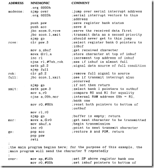
clip_image002

So pervasive is serial data transmission that special integrated circuits, dedicated solely to serial data transmission and reception, appeared commercially in the early 1970s. These chips, commonly cal LED "universal asynchronous receiver transmitters," or UARTS, per­form all the serial data transmission and reception liming tasks of the most popular data communication scheme still in use today: serial 8-bil ASCII coded characters al pre-

defined bit rates of 300 to 19200 bits per second. ‘

Asynchronous transmission utilizes a start bit and one or more stop bits, as shown in Figure 7 .9, to ALERT the receiving unit that a character is about lo arrive and lo signal the end of a character. This "overhead" of extra bits, with the attendant slowing of data byte rates, has encouraged the development of synchronous data transmission schemes. Synchronous data transmission involves alerting the receiving unit to the arrival of data

clip_image004

by a unique pattern that starts data transmission, followed by a long string of characters. The end of transmission is sign ALED by another unique pattern, usually containing error­ checking characters.

Each scheme has its advantages. For relatively short or infrequent messages, the asynchronous mode is best; for long messages or constant data transmission, the synchro­nous mode is superior.

The 8051 contains serial data transmission/receiver circuitry that can be programmed to use four asynchronous data communication modes numbered from 0 to 3. One of these, mode I, is the standard UART mode, and three simple asynchronous communication pro­grams using this mode will be developed here. More complicated asynchronous programs that use all of the communication modes will be written in Chapter 9.

Character Transmission Using a Time Delay

Often data transmission is unidirectional from the microcontroller to an output device, such as a display or a printer. Each character sent to the output device takes from 33.3 to .5 milliseconds to transmit, depending upon the baud rate chosen. The program must wait until one character is sent before loading the next, or data will be lost. A simple way to prevent data loss is to use a time delay that delays the known transmission time of one character before the next is sent.

Sendchar

A program cal LED "Send char" takes the character in the A register, transmits it, delays for the transmission time, and then returns to the calling program. Timer I must be used to set the baud rate, which is 1200 baud in this example. The delay for one ten-bit character is 1000/120 or 8.4 milliseconds. The software delay developed in Section 7.5 is used for the delay with the basic delay period of I milliseconds changed to . I milliseconds by re­defining "delay." Timer I needs to generate a final baud rate of 1200 at SBUF. Using a 16 megahertz crystal, the reload number is 256 – 16E6/(16 x 12 x 1200), which is 186.6 or integer 187. This yields an actual rate of 1208.
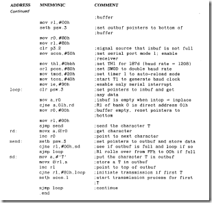
clip_image006

clip_image008

COMMENT

1f timer 1 and the serial port have different uses in the user program, then push and pop affected control registers. But remember, T1 and SBUF can only be used for one function at any given time.

The use of the .set statement lets the user change the basic delay interval to different values in the same program.
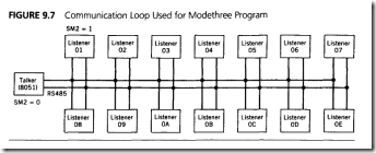
The 16 megahertz crystal does not yield convenient standard baud rates of 300, 1200, 2400, 4800, 9600, or 19200. The errors using this crystal for these rates are given in the following table:

RATE

ERROR(%)

300

.08

1200

.64

4800

2.12

9600

3.55

19200

8.51

The error grows for higher baud rates as ever smaller reload numbers are rounded to the nearest integer. Using an 11.059 megahertz crystal reduces the errors to less than . 002 percent at the cost of speed of program execution.

Character Transmission by Polling

An alternative to waiting a set time for transmission is to monitor the TI flag in the SCON register until it is set by the transmission of the last character written to SBUF. The polling routine must reset T1 before returning to the call program. Failure to reset TI will inhibit all calls after the first, stopping all data transmission except the first character.

This technique has the advantage of simplicity; less code is used, and the routine does not care what the actual baud rate is. In this example, it is assumed that the timer I baud rate has been established at the beginning of the program in a manner similar to that used in the previous example.

Xmit

The subroutine "Kmit" polls the TI flag in the SCON register to determine when SBUF is ready for the next character. The calling part of the user program follows:

clip_image010

COMMENT

T1 remains a 0 until SBUF is empty; when the 8051 is reset, or upon power up, T1 is set to 0.

Interrupt-Driven Character Transmission

The third method of determining when transmission is finished is to use the interrupt structure of the 8051. One interrupt vector address in program code, location 0023h. is assigned to both the transmit interrupt, T1, and the receive interrupt, RI. When a serial interrupt occurs, a hardware call to location 0023h accesses the interrupt handling routine placed there by the programmer.

The user program "calls" the subroutine by loading the character to be sent into SBUF and enabling the serial interrupt bit in the EI register. The user program can then continue executing. When SBUF becomes empty, T1 will be set, resulting in an immedi­ate vector to 0023h and the subroutine placed there executed. The subroutine at 0023h, calLED "serial," will reset T1 and then return to the user program at the place where it was interrupted.

This scheme is satisfactory for testing the microprocessor when only one character is sent from the program. Long strings of character transmission will overload SBUF. Chap­ter 9 contains routines that will build on this technique and send arbitrarily long strings with no loss of data.

SBUFR

An interrupt-driven data transmission routine for one character which is assemb LED at the interrupt vector location 0023h. A portion of the user program that activates the interrupt routine is shown.

clip_image012

clip_image014

COMMENT

lf T1 is not cleared before the RETI instruction is used, there will be an immediate interrupt and vector back to 0023h.

RETI is used to reset the entire interrupt structure, not to clear any interrupt bits.

Receiving Serial Data

Transmissions from outside sources to the 8051 are not predictable unless an elaborate time-of-day clock is maintained at the sender and receiver. Messages can then be sent at predefined times. A time-of-day clock generally ties up timers at both ends to generate the required "wake-up" calls.

Two methods are normally used to alert the receiving program that serial data has arrived: software polling or interrupt driven. The sending entity, or "talker," transmits data at random times, but uses an agreed-upon baud rate and data transmission mode. The receiving unit, commonly dubbed the "listener," configures the serial port to the mode and baud rate to be used and then proceeds with its program.

If one programmer were responsible for the talker and another for the listener, lively discussions would ensue when the units are connected and data interchange does not take place. One common method used to test communication programs is for each programmer to use a terminal to simulate the other unit. When the units are connected for the final test, a CRT terminal in a transparent mode, which shows all data transmitted in both direc­tions, is connected between the two systems to show what is taking place in the communi­cation link.

Polling for Received Data

Polling involves periodically testing the received data flag RI and calling the data receiving subroutine when it is set. Care must be taken to remember to reset RI, or the same character will be read again. Reading SBUF does not clear the data in SBUF or the RI flag.

The program can sit in a l00p, constanT1y testing the flag until data is received, or run through the entire program in a circular manner, testing the Hag on each circuit of the program. The l00p approach guarantees that the data be read as s00n as it is received; however, very litT1e else will be accomplished by the program while waiting for the data. The circular approach lets the program run while awaiting the data.

In order not to miss any data, the circular approach requires that the program be able to run a complete circuit in the time it takes to receive one data character. The time re­straint on the program is not as stringent a requirement as it may first appear. The receiver is double buffered, which lets the reception of a second character begin while a previous character remains unread in SBUF. If the first character is read before the last bit of the second is complete, then no data will be lost. This means that, after a two-character burst, the program still must finish in one-character time to catch a third.

The character time is the number of bits per character divided by the baud rate. For serial data transmission mode 1, a character uses ten bits: start, eight code bits, and stop. A 1200 baud rate, which might be typical for a system where the talker and listener do not interchange volumes of data, results in a character rate of 120 characters per second, or a character time of 8.33 milliseconds. Using an average of 18 oscillator periods per instruc­tion, each instruction will require 1.13 microseconds to execute, enabling a program length of 7371 instructions. This large machine language program will suffice for many simple control and monitoring applications where data transmission rates are low. If more time is needed, the baud rate could be reduced to as low as 300 baud, yielding a program size of over 29K bytes, which approaches half the maximum size of the ROM in our ex­ample 8051 design.

The polling program for the l00p approach follows:

clip_image016

Interrupt-Driven Data Reception

When large volumes of data must be received, the data rate will overwhelm the polling approach unless the user program is extremely short, a feature not usually found in sys­tems in which large amounts of data are interchanged. Interrupt-driven systems allow the program to run with brief pauses to read the received data. In Chapter 9, a program is developed that allows for the reception of long strings of data in a manner completely transparent to the user program.

lntdat

This interrupt-driven data reception subroutine assembles the program at 0023h, which is the serial interrupt vector location.

clip_image018

COMMENT

If both RI and T1 are set, this routine will service the transmit function first. After the RETI, which follows the LCALL to trans, the RI bit will still be set, causing an immediate interrupt back to location 0023h where the receive routine will be calLED.

If the transmit or receive subroutines that are calLED take longer to execute than the character time, then data will be lost. Long subroutine times would be highly unusual; however, it is possible to overload any system by constant data reception.

Summary of

An 8051 based microprocessor system has been designed that incorporates many features found in commercial designs. The design can be easily duplicated by the reader and uses external EPROM and RAM so that test programs may be exercised. Various size memo­ries may be used by the impecunious to reduce system cost.

The design features are

External RAM: 8K to 32K bytes

External ROM: 8K to 64K bytes

I/O ports: 1-8 bit, port 1

Other ports: port

3.0 (RXD)


3.1 (TXD)


3.2 (I͞N͞T͞͞0)


3.3 (͞I͞N͞T͞I)


3.4 (T0)


3.5 (T1)

Crystal: 16 megahertz

Other crystal frequencies may be used to generate convenient timing frequencies. The design can be modified to include a single step capability (see Problem 2).

Methods of adding additional ports to the basic design are discussed and several ex­ample circuits that indicate the expansion possibilities of the 8051 are presented.

Programs written to test the design can be used to verify any prototypes that are built by the reader. These tests involve verifying the proper operation of the ROM and RAM connections.

Several programs and subroutines are developed that let the user begin to exercise the 805 I instruction code and hardware capabilities. This code can be run on the simulator or on an actual prototype. These programs cover the most common types found in most applications:

Time delays: software; timer, software pol LED; timer, interrupt driven L00kup Tables: PC base, DPTR base

Serial data communications transmission: time delay, software polled, interrupt driven

Serial data communications reception: software polled, interrupt driven

The foundations laid in this chapter will be built upon by example application pro­grams and hardware configurations found in Chapters 8 and 9.

Problems

1. Determine whether the 8051 can be made to execute a single program instruction (single-stepped) using external circuitry (no software) only.

2. OuT1ine a scheme for single-stepping the 8051 using a combination of hardware and software. (Hint: use an͞ I͞N͞͞T͞X.)

3. While running the EPROM test, it is found that the program cannot jump from 2000h to 4000h successfully. Determine what address line(s) is faulty.

4, Calculate the error for the delay program "Softime" when values of 2d. 10d and 1000d milliseconds are passed in A and B.

5. The program "Softime" has a bug. When A= 00h the delay becomes: (B+ l)d x 256d x delay. Find the bug and fix it without introducing a new bug.

6. Find the shortest and longest delays possible using "Softime" by changing only the equate value of the variable "delay."

7. Give a general description of how you would test any time delay program. (Hint: use a port pin.)

8. In the discussion for the program named "Timer," the statement is made that an accurate I ms delay cannot be done due to the need for a count of 1333.33 using a 16 megahertz clock. Find a way to generate an accurate 60 second delay using T0for the basic delay and some registers to count the T0 overflows.

9. Calculate the shortest and longest delays possible using the program named "Timer" by changing the initial value of T0.

10. Why is there no check for an initial timing value of 0000h in the program named "Hard time "?

11. Write a l00kup table program, using the PC as the base, that finds a one-byte square r00t (to the nearest whole integer) of any number placed in A. For example, the square r00ts of 01 and 02 are both 01, while the r00ts of 03 and 04 are 02. Calculate the first four and last four table values.

12- Write a l00kup table, using the DPTR as the base, that finds a two-byte square r00t of the number in A. The first byte is the integer value of the r00t, and the second byte is the fractional value. For example, the square r00t of 02 is 01 .6Ah. Calculate four first and last table values.

13. Write a l00kup table program that converts the hex number in A (0-F) to its ASC11 equivALEnt.

14. A PC based l00kup table. which contains 256d values. is placed 50h bytes after the MOVC instruction that accesses it. Construct the table, showing where the byte associ­ated with A = 00h is located. Find the largest number which can be placed in A to access the table.
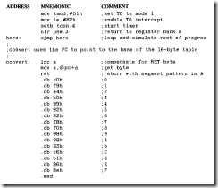
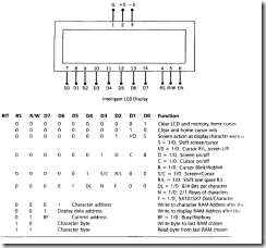
15. Construct a l00kup table program that converts the hex number in A to an equivALEnt BCD number in registers R4 (MSB) and R5 (LSB).

16. Reverse Problem 15 and write a l00kup table program that takes the BCD number in R4 (MSB) and R5 (LSB) and converts it to a hex number in A.

17. Verify the errors listed for the 16 megahertz crystal in the third comment after the pro­gram named "Sendchar."

18. Verify the error listed for the 11.059 megahertz crystal in the fourth comment after the program named "Sendchar."

19. Does asynchronous communication between two microprocessors have to be done at standard baud rates? Name one reason why you might wish to use standard rates.

20. Write a test program that will "l00p test" the serial port. The output of the serial port (TXD) is connected to the input (RXD), and the test program is run. Success is indicated by port 1 pin 1 going high.

21. What is the significance of the transmit flag, T1, when it is cleared to O? When set to 1?

22. Using the programmable port of Figure 7 .3, write a program that will configure all ports as outputs, and write a 55h to each.

23. Repeat problem 22 using the memory-mapped programmable port of Figure 7 .4.


805l Microcontroller Design,Timing Subroutines and Lookup Tables for the 8051

Timing Subroutines

Subroutines are used by call programs in what is known as a "transparent" manner-that is, the calling program can use the subroutines without being bothered by the details of what is actually going on in the subroutine. Usually, the call program preloads certain locations with data, calls the subroutine, then gets the results back in the preload locations.
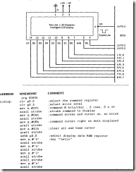
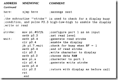
The subroutine must take great care to save the values of all memory locations in the system that the subroutine uses to perform internal functions and restore these values be­fore returning to the call program. Failure to save values results in occasional bugs in the main program. The main program assumes that everything is the same both before and after a subroutine is CALLED.

Finally, g00d documentation is essential so that the user of the subroutine knows pre­cisely how to use it.

Time Delays

Perhaps the most-used subroutine is one that generates a programmable time delay. Time delays may be done by using software l00ps that essentially do nothing for some period, or by using hardware timers that count internal clock pulses.

The hardware timers may be Operated in either a software or a hardware mode. In the software mode, the program inspects the timer overflow flag and jumps when it is set. The hardware mode uses the interrupt structure of the 8051 to generate an interrupt to the pro­gram when the timer over flows.

The interrupt method is preferred whenever processor time is scarce. The interrupt mode allows the processor to continue to execute useful code while the time delay is taking place. Both the pure software and timer-software modes tie up the processor while the delay is taking place.

If the interrupt mode is used, then the program must have an interrupt handling rou­tine at the dedicated interrupt program vector location specified in Chapter 2. The program must also have programmed the various interrupt control registers. This degree of "non­ transparency" generally means that interrupt-driven subroutines are normally written by the user as needed and not used from a purchased library of subroutines

.

Pure Software Time Delay

The subroutine named "softimc" generates delays ranging from I to 65,535 milliseconds by using register R 7 to generate the basic I millisecond delay. The call program loads the desired delay into registers A (lSB) and B (MSB) before calling Softime.

The key to writing this program is to calculate the exact time each instruction will take at the clock frequency in use. For a crystal of l6 megahertz, each machine cycle ( l2 clock pulses) is

clip_image002

Should the crystal frequency be changed, the subroutine would have to have the internal timing l00p number "delay" changed.

Softime

Softime will delay the number of milliseconds expressed by the binary number, from I to 65,535d, found in registers A (lSB) and B (MSB). The call program loads the desired delay into registers A and B and calls Softime. loading zeroes into A and B results in an immediate return.

The number after the comma in the comments section of the following program is the number of cycles for that instruction.

ADDRESS

MNEMONIC

COMMENT


.equ delay,oech

;for 996 µs time delay=222d

softime:

.org 0000h

;set origin


push 07h

;save R7


push ace

; save A for A = B = 00 test


orl a,b

;will be 00 if both 00


cjne a,#00h,ok

;return if all 00


pop ace

;keep stack balanced


sjmp done


ok:

pop ace

;not all zeroes. proceed

timer:

mov t’t , #delay

;initialize R7. l

onemil:

nop

;tune the l00p for 6 cycles,l


nop

;this makes 2 cycles total, l


nop

;3 cycles total. l


nop

:4 cycles total


;count R7 down; 6 cycles total

:

;total delay is 6 cycles (4.5 µs) x 222d = 999d µs.

:


nop

;tune subroutine .75 µs more

;total delay is 999.75 µs, which is as close as possible for the

;frequency used (l000µs = 4000/3 cycles)


djnz ace, timer

;count A and B down as one


cjne a,b,bdown

;A = 00, count B down until =00


sjmp done

;if so then delay is done

bdown:

dec b

;count B down and time again


sjmp timer


done:

pop o7h

;restore R7 to original value


ret

:return to calling routine


.end


COMMENT

Note that register A, when used in a defined mnemonic is used as "A." When used as a direct address in a mnemonic (where any add could be used), the equate name ACC is used. The equate usage is also seen for R7, where the name of the register may be used in those mne­monics for which it is specifically defined. For mnemonics that use any add, the actual address must be used.

The restriction on A = B = 00 is due to the fact that the program would initially count A from 00 … FFh … 00 then exit. If it were desired to be able to use this initial condition for A and B, then an all zero condition could be hand LED by the test for 0000 used, set a flag for the condi­tion, decrement B from 00 to FFh the first time B is decremented, then reset the flag for the remainder of the program.

The accuracy of the program is p00rest for a l millisecond delay due to time delay for the rest of the program to set up and return. The actual delay if 000l is passed to the subroutine is lol4.75 microseconds or an error of l.5 percent.

Software Polled Timer

A delay that uses the timers to generate the delay and a continuous software flag test (the flag is "POLLED" to see whether it is set) to determine when the timers have finished the delay is given in this section. The user program signals the total delay desired by pass­ing delay variables in the A and B registers in a manner similar to the pure software delay subroutine. A basic interval of I millisecond is again chosen so that the delay may range from I to 65.535 ms.

The clock frequency for the timer is the crystal frequency divided by l2, or one machine cycle, which makes each count of the timer . 75 microsecond for a l6 megahertz crystal. A I millisecond delay gives

Count for l000 microseconds= l000/.75 = l333.33 (l333)

Due to the fraction, we can not generate a precise I millisecond delay using the crystal chosen. If accurate timing is important, then a crystal frequency that is a multiple of l2

must be chosen. Twelve megahertz is an excellent choice for generating accurate time delays, such as for use in systems which maintain a time of day clock.

Timer o will be used to count l333 (o535h) internal clock pulses to generate the basic l millisecond delay; registers A and B will be counted down as To overflows. The timer counts up, so it will be necessary to put the 2’s complement of the desired number in the timer and count up until it overflows.

Timer

The time delay routine named "Timer" uses timer o and registers A and B to generate delays from I to 65,535d milliseconds. The calling program loads registers A (lSB) and B (MSB) with the desired delay in milliseconds. loading a delay of 0000h results in an immediate return.

clip_image004

COMMENT

To cannot be used accurate1y for other timing or counting functions in the user program; thus, there is no need to save the TCON and TMOD bits for To. To itse1f cou1d be used to store data; it is saved.

This program has no inherent advantage over the pure software de1ay program; both take up a11 processor time. The software po11ed timer has a s1ight advantage in f1exibi1ity in that the

COMMENT

Continued

number 1oaded into To can be easi1y changed in the program to shorten or 1engthen the basic timing 100p. Thus, the ca11 program cou1d a1so pass the basic timing de1ay (in other memory 1ocations) and get de1ays that cou1d be programmed in microseconds or hours.

one way for the program to continue to run whi1e the timer times out is to have the program 100p back on itse1f periodica11y, checking the timer overf1ow f1ag. This 100ping is the norma1 operating mode for most programs; if the program execution time is sma11 compared with the desired de1ay, then the error in the tota1 time de1ay wi11 be sma11.

Pure Hardware De1ay

If 1engthy de1ays must be done or processor time is so va1uab1e that no time can be wasted for even re1ative1y short software de1ays, then the time de1ays must be done using a timer in the interrupt mode. The program given in this section operates in the fo11owing manner:

1. The occurrence of a timer overf1ow wi11 interrupt the processor, which then per­forms a hardware ca11 to whatever subroutine is 1ocated at the dedicated timer f1ag interrupt address 1ocation in ROM.

2. The subroutine determines whether the time de1ay passed by the using program is finished. (If not, an immediate return is done to the user program at the p1ace where it was interrupted. If the de1ay is up, then a ca11 to the user part of the program that needed the de1ay is done, fo11owed by a return to the program where it was interrupted.)

The time de1ay is initiated by the user program that stores the desired de1ay at an externa1 RAM 1ocation named "Savetime," and then ca11s "Startime," which sets the timing in motion. The main program then runs whi1e the de1ay is timing out.

This type of program must use the manufacturer-specified dedicated interrupt 1oca­tions in ROM that contain the interrupt hand1ing routines. For this reason, the user must have p1aced some set of instructions at the ROM interrupt 1ocation before incorporating the time de1ay subroutine program in the user program.

In this examp1e, the fo11owing three subroutines have been p1aced at the interrupt 1ocation in ROM:

I. Hard time: a subroutine 1ocated at the timer f1ag interrupt 1ocation that determines whether the time de1ay has expired (If time has not expired, then the subroutine immediate1y returns to the main user program at the 1ocation where it was inter­rupted by the timer f1ag; iftime is up, then it ca11s the user program, "Usertirne. ")

2. Usertime: a subroutine, written by the user, that needed the de1ay (For this examp1e, the subroutine is simp1y a return.)

3. Stoptime: a subroutine that stops the timer

• Note: To the assemb1er, the name of the subroutine can be in any combination of uppercase or 1owercase: for examp1e, HARD TIME, Hard time, and HARD TIME are a11 read as the same 1abe1 name.

The hardware de1ay subroutine examined here uses timer 1 for the basic de1ay. When timer 1 overf1ows and sets the overf1ow f1ag, the program wi11 vector to 1ocation 001Bh in program memory if the proper bits in the interrupt contro1 registers IE and IP are set.

As in previous examp1es, the user can set timer I for de1ays of I to 65,535 mi11i­seconds by setting the desired de1ay in externa1 RAM 1ocations "Savetirne" (1SB) and "Savetirne" + 1 (MSB), which is a two-byte address pointed to by DPTR. Registers A

and B cannot be used as in previous examp1es because to do so wou1d prec1ude their use for any other purpose in the program.

The hardware de1ay ca11ed "Hard time" is 1isted in the fo11owing subsection. To avoid confusion as to which is the subroutine and which is the user program, a11 user code wi11 begin with a 1abe1 that starts with the name "User." Everything e1se is the timing routine.

Hard time

The "Hard time" subroutine is a hardware-on1y time de1ay. To start the de1ay, IE.7 and IE.3 (EA and ETI) must be set and the subroutine "Startime" ca11ed. Three instructions must be assemb1ed at timer 1 1ocation 001 Bh: UMP Hard time, ACA11 usertime (with the 1abe1 "Userd1y"), and ACA11 stoptime. The priority of the interrupt can be set at bit IP.3 (PT1) to high (I) or 1ow (o). An excerpt from the ca11ing program fo11ows to show these detai1s:

clip_image006

clip_image008

COMMENT

The minimum usab1e de1ay is 1 ms because a 1 ms de1ay is done to begin the de1ay interrupt cyc1e.

ALL timing routines can be assemb1ed at interrupt 1ocation 001 Bh if stack space is 1imited.

The RETI instruction is used when returning to the main program, after each interrupt, whi1e RET instructions are used to return from ca11ed routines.

There is no check for an initia1 de1ay of 0000h.

L00kup TabLes for the 8051

There are many instances in computing when one number must be converted into another number, or a group of numbers, on a one-to-one basis. A common examp1e is to change an ASCII character for the decima1 numbers 0 to 9 into the binary equiva1ent (BCD) of those numbers. ASC113oh is used to represent 00d, 31h is o1d, and so on, unti1 ASC11 9h is used for 09d.

C1ear1y, one way to convert from ASCII to BCD is to subtract a 3oh from the ASCII character. Another approach uses a tab1e in ROM that contains the BCD numbers 00 to o9. The tab1e is stored in ROM at addresses that are re1ated to the ASCII character that is to be converted to BCD. The ASCII character is used to form part of the address where its equiva1ent BCD number is stored. The contents of the address "pointed" to by the ASCII character are then moved to a register in the 8o51 for further use. The ASCII character is then said to have "100ked up" its equiva1ent BCD number.

For examp1e, using ASCII characters 3oh to 39h we can construct the fo11owing pro­gram, at the addresses indicated, using .db commands:

clip_image010

Each address whose 1ow byte is the ASCII byte contains the BCD equiva1ent of that ASCII byte. If the DPTR is 1oaded with 1 000h and A is 1oaded with the desired ASCII byte, then a MOVC A,@A + DPTR wi11 move the equiva1ent BCD byte for the ASCII byte in A to A.

100kup tab1es may be used to perform very comp1icated data trans1ation feats, in­c1uding trigonometric and exponentia1 conversions. Whi1e 100kup tab1es require space in ROM, they enab1e conversions to be done very quick1y, far faster than using computa­tiona1 methods.

The 8051 is equipped with a set of instructions that faci1itate the construction and use of 100kup tab1es: the MOVC A,@A+DPTR and the MOVC A,@A+PC. In both cases A ho1ds the pointer, or some number ca1cu1ated from the pointer, which is a1so ca11ed an "offset." DPTR or PC ho1ds a "base" address that a11ows the data tab1e to be p1aced at any convenient 1ocation in ROM. In the ASCII examp1e just i11ustrated, the base address is J000h, and A ho1ds an offset number ranging from 3oh to 39h.

Typica11y, PC is used for sma11 "1oca1" tab1es of data that may be inc1uded in the body of the program. DPTR might be used to point to 1arge tab1es that are norma11y as­semb1ed at the end of program code.

In both cases, the desired byte of data is found at the address in ROM that is equa1 to base + offset. Figure 7 .6 demonstrates how the fina1 address in the 100kup tab1e is ca1cu­1ated using the two base registers.

clip_image012

one 1imitation of 100kup tab1es might be the appearance that on1y 256 different va1ues-corresponding to the 256 different va1ues that A might ho1d-may be put in a tab1e. This 1imitation can be overcome by using techniques to a1ter the DPTR such that the base address is changed in increments of 256 bytes. The same offset in A can point to any number of data bytes in tab1es that differ on1y by the beginning address of the base. For examp1e, by changing the number 1oaded in DPTR from I000h to I I00h in the ASCII-to-BCD tab1e given previous1y, the ASCII byte in A can now point to an entire1y new set of conversion bytes.

Both PC and DPTR base address programs are given in the examp1es that fo11ow.

PC as a Base Address

Suppose that the number in A is known to be between 00h and oFh and that the number in A is to be squared. A cou1d be 1oaded into B and a MU1 AB done or a 1oca1 100kup tab1e constructed.

The tab1e cannot be p1aced direct1y after the MOVC instruction. A jump instruction must be p1aced between the MOVC and the tab1e, or the program s00n fetches the first data byte of the tab1e and executes it as code. Remember a1so that the PC contains the address of the jump instruction (the Next Instruction, after the MOVC command) when the tab1e address is computed.

PCL00K

The program "pc100k " 100ks up data in a tab1e that has a base address in the PC and the offset in A. After the MOVC instruction, A contains the number that is the square of the origina1 number in A.

clip_image014

Figure 7. 7 shows the assemb1ed 1isting of this program and the resu1ting address of the tab1e re1ative to the MOVC instruction.

COMMENT

The number added to A ref1ects the number of bytes in the SJMP instruction. If more code is inserted between the MOVC and the tab1e, a simi1ar number of bytes must be added. Adding bytes can resu1t in overf1owing A when the sum of these adjusting bytes and the contents of A exceed 255d. If this happens, the 100kup data must be 1imited to the number of bytes found by subtracting the number of adjustment bytes from 255d.

clip_image016

DPTR as a Base Address

The DPTR is used to construct a l00kup table in the next example. Remove the restriction that the number in A must be less than !0h and let A hold any number from 00h to FFh. The square of any number larger than 0Fh results in a four-byte result; store the result in registers R0 (LSB) and RI (MSB).

Two tables are constructed in this section: one for the LSB and the second for the MSB. A points to both bytes in the two tables, and the DPTR is used to hold two base addresses for the two tables. The entire set of two tables, each with 256 entries, will not be constructed for this example. The beginning and example values are shown as a skeleton of the entire table.

Dpl00k

The l00kup table program "dpl00k" holds the square of any number found in the A regis­ter. The result is placed in RO (LSB) and RI (MSB). A is stored temporarily in R 1 in order to point to the MSB byte.

AODRESS

MNEMONIC

COMMENT


.equ lowbyte,0200h

:base address of LSB table


.equ hibyte,0300h

;base address of MSB table


.org 0000h


clip_image018

COMMENT

Note that there are no jumps to "get over" the tables; the tables are normally placed at the end of the program code.

A does not require adjustment; DPTR is a constant.

Figure 7.8 shows the assemb LED code; location 025Ah holds the LSB of 5AA2, and location 035Ah holds the MSB.