Feedback and Sequential Circuits :Flip Flops (RS and JK) and Edge Triggered Flip Flops

Feedback and Sequential Circuits

This chapter’s title probably seems like a bit of a misnomer; you are probably wondering what feedback has to do with digital electronics? When I use the term ‘‘feedback’’, I am using it in the most literal sense, past state data are used to maintain current state data. These circuits built from the theory that I am going to provide in this chapter are commonly known as ‘‘memory devices’’. For digital electronic circuits to store information, that information will continually move through the circuit and is used to determine what the future value of the circuit is. Feedback is critical to provide digital electronics with the ability to ‘‘remember’’ previous states and data.

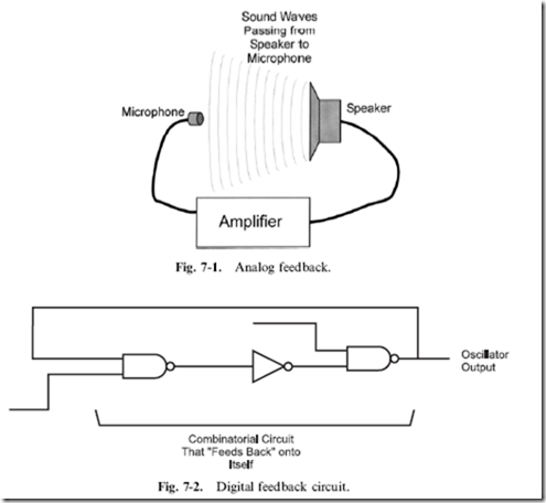
When you first hear the term ‘‘feedback’’, you probably think of an

amplifier with its microphone input brought close to its speaker output (Fig. 7-1). You also probably involuntarily wince at the thought of the term ‘‘feedback’’ because it brings back the memory of the horrible sound the amplifier made when the microphone was too close. This type of feedback

image

cannot save information; the uncontrolled amplification of the signal distorts and destroys information in a very short order.

When I introduced combinatorial circuits at the start of the book, I noted

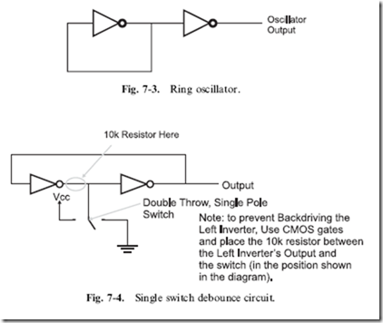
that an important part of combinatorial circuits was that data could only travel in one path; no outputs were passed back to earlier inputs in a logic chain, like the one shown in Fig. 7-2. The reason for specifying that outputs were not to be passed to inputs was to make sure that an inadvertent oscillator, known as a ‘‘ring oscillator’’ (Fig. 7-3), was not created.

You should know that the inverter in Fig. 7-3 is going to invert its input. The problem arises when the input is tied to the output, as it is in this case. When the input is passed to the inverter, it outputs the inverted value, which is then immediately passed back to the input and the gate inverts the value again, and again, and so on.

image

The ring oscillator is probably the simplest oscillator that you can build and the period of the oscillation runs at literally the speed of the technology’s gate delay times the number of gate delays. If the ring oscillator shown in Fig. 7-3 was built from TTL (which has a gate delay of 8 ns) you would see a ‘‘square wave’’ with a period of 62.5 MHz. One of the functions that ring oscillators perform is the measurement of a logic technology’s gate delay.

Extrapolating from what has been discussed here, you could build a simple memory circuit using the two inverters and a double throw switch, wired as shown in Fig. 7-4. This circuit is used to ‘‘debounce’’ a switch input. As I will discuss in later chapters, when a mechanical switch is thrown, the physical contacts within the switch literally bounce against each other before a hard, stable contact is made. This bouncing can cause quite a bit of grief when you are trying to respond to a single switch movement.

The circuit in Fig. 7-4 will pass a signal continuously between the two

inverters (the output of the two inverters is the same as the input, so there is no chance for a ring oscillator) until the switch comes in contact with a connection that forces the state to change. If the switch was originally at the ground position, the signal coming from the inverter to its left would be a ‘‘0’’. When the switch was moved to the ‘‘Vcc’’ position, the signal going to the inverter to the right would be changed and its output would change.

The beauty of this circuit is that when the switch is in between contacts, the output state of the circuit remains constant.

When the switch is not touching either contact, the two inverters are maintaining the previous bit value and the circuit behaves essentially as a memory device.

There is a downside to the button debounce circuit in Fig. 7-4 and that is when the switch is thrown, it connects the left inverter output to the opposite power supply that it is driving out. This is known as ‘‘backdriving’’ and it should always be avoided.

Backdriving a gate will shorten its life in the best case and could burn it out in very short order. As noted in Fig. 7-4, you should only use CMOS inverters (which are voltage, rather than current controlled) and place the 10 k resistor between the switch and the output of the left inverter. By using this circuit, there will be no chance that the left inverter’s output is tied directly to power or ground (which will be the opposite value that it’s at) and the 10 k resistor will limit the amount of current that is passed. I did not put the resistor into Fig. 7-4 as it is a basic circuit that I have seen in a number of references and I wanted to point out that it does backdrive a gate output and there are ways of avoiding this problem.

The other term used in this chapter’s title, ‘‘sequential circuits’’, is used to

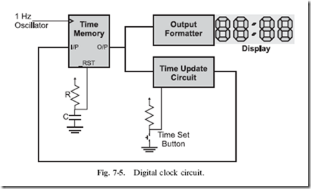
identify the class of digital electronic circuits that have memory devices within them and use their data, along with combinatorial circuits, to produce applications. A digital clock (Fig. 7-5) is an excellent example of a sequential circuit. The data output from the memory circuits of the clock are passed to

image

combinatorial logic circuits and the outputs of the combinatorial circuits are passed back to the inputs of the ‘‘time memory’’ circuits.

Any time memory circuits, like the ones presented in this chapter, are used in a digital electronics application, the circuit is called a ‘‘sequential circuit’’.

Flip Flops (RS and JK)

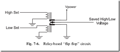
The best analogy I can find for a simple, one bit ‘‘memory device’’ is the two coiled relay of Fig. 7-6. The relay coil does not have a return spring that only one coil pulls against; when the relay’s wiper is placed in a position it stays there. This memory device is set to one of two states, depending on which relay coil was last energized, pulling the wiper contact into connection with it. Once electricity to the coil is stopped, the memory device will stay in this state until the other coil is energized and the wiper is pulled towards it. This device works very similarly to the most basic electronic memory device that you will work with, the ‘‘reset-set’’ (RS) ‘‘flip flop’’.

The term ‘‘flip flop’’ is indicative of the operation of the memory device: it

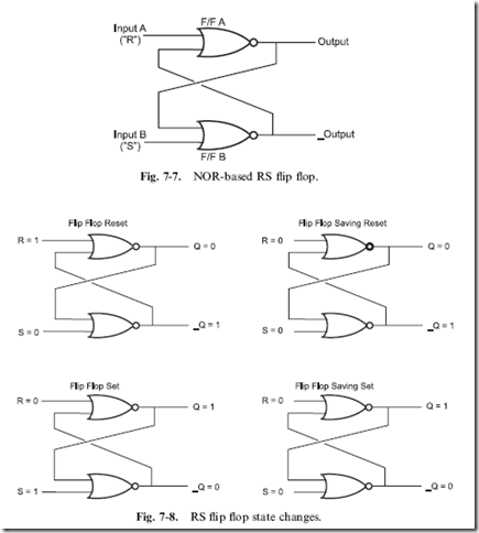
is either ‘‘flipped’’ to one value or ‘‘flopped’’ to another. Where the relay device relies on friction to keep the saved value constant, the electronic memory unit takes advantage of feedback to store the value. Digital feedback can only be one of two values, so its use in circuits probably seems like it is much more limited than that of analog feedback. This is true, except when it is used as a method to store a result in a circuit like the ‘‘NOR flip flop’’, shown in Fig. 7-7. Normally, the two inputs are at low voltage levels, except to change its state, in which case one of the inputs is raised to a high logic level.

If you are looking at this circuit for the first time, then it probably seems like an improbable device, one that will potentially oscillate because if the output value of one gate is passed to the other and that output is passed to

image


image

the original, it seems logical that a changing value will loop between the two gates. Fortunately, this is not the case; instead, once a value is placed in this circuit, it will stay there until it is changed or power to the circuit is taken away. Figure 7-8 shows how by raising one pin at a time, the output values of the two NOR gates are changed.

When the ‘‘R’’ and ‘‘S’’ inputs to their respective NOR gates are low, there is only one signal left that will affect the output of the NOR gates and that is output of the other NOR gate. When ‘‘Q’’ is low, then a low voltage will be passed to the other NOR gate. The other NOR gate outputs a high voltage because its other input is low. This high signal is passed to the original

NOR gate and causes it to output a low voltage level, which is passed to the other NOR gate and so on.. . .

The outputs of the flip flop are labeled as ‘‘Q’’ and ‘‘_Q’’. ‘‘Q’’ is the positive output while ‘‘_Q’’ is the negative value of ‘‘Q’’ – exactly the same as if it were passed through an inverter. The underscore character (‘‘_’’) in front of the output label (‘‘Q’’) indicates that the signal is inverted (the same as if an exclamation mark (‘‘!’’) is used for an inverter’s output). When you look at some chip diagrams, you will see some inputs and outputs that have the underscore before or on the line above the pin label.

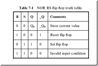
The ‘‘R’’ and ‘‘S’’ input pins of the flip flop are known as the ‘‘reset’’ and ‘‘set’’ pins, respectively. When the ‘‘R’’ input is driven high the ‘‘Q’’ output will be low and when ‘‘S’’ is high the ‘‘Q’’ output will be driven high. These values for ‘‘Q’’ will be saved when ‘‘R’’ and ‘‘S’’ are returned to the normal low voltage levels. ‘‘Q0’’ and ‘‘_Q0’’ are the conventional shorthand to indicate the previous values for the two bits and indicates that the current values of ‘‘Q’’ and ‘‘_Q’’ are the same as the previous values. Truth tables are often used to describe the operation of flip flops and the truth table for the NOR RS flip flop is given in Table 7-1.

In Table 7-1, I have marked that if both ‘‘R’’ and ‘‘S’’ were high, while the outputs are both low, the inputs were invalid. The reason why they are considered invalid is because of what happens when R and S are driven low. If one line is driven slower than the other, then the flip flop will store its state. If both R and S are driven low at exactly the same time (not a trivial feat), then the flip flop will be in a ‘‘metastable’’ state, Q being neither high nor low, but anything that disturbs this balance will cause the flip flop to change to that state. The metastable state, while seemingly useless and undesirable is actually very effective as a ‘‘charge amplifier’’ – it can be used to detect very

image

image

small charges in capacitors. This is an important mode of operation that is taken advantage of for DRAM and SDRAM memories.

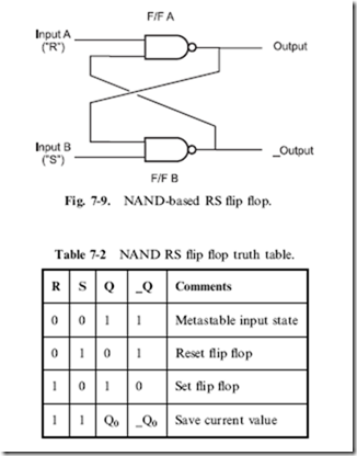
Along with building a flip flop out of NOR gates, you can also build one out of NAND gates (Fig. 7-9). This circuit works similarly to the NOR gate, except that its metastable state occurs when both inputs are low, and the inputs are active at low voltage levels, as I have shown in Table 7-2, which is the NAND RS flip flop’s truth table.

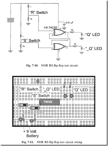
You can build your own NOR RS flip flop, which has its state set by two switches as I show in Fig. 7-10 and is wired according to Fig. 7-11.

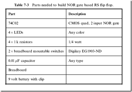
I suggest that you test out the circuit in as many different ways as possible – especially investigating the metastable and post-metastable states. Unless you were to wire the R and S inputs to one switch, you will find it impossible to achieve the metastable state. The parts that are needed to build the RS flip flop are listed in Table 7-3.

Before going on, there is one additional point about flip flops that may not be immediately obvious but will be something that you will have to consider

image

in your career as a designer of digital electronic devices; when power is removed, the flip flops will lose the bit information contained within them. The term used to describe this phenomena is ‘‘volatility’’; flip flops are considered ‘‘volatile’’ devices. Flash memory (like the flash used in your PC) does not lose its information when power is shut off and is known as ‘‘non-volatile’’ memory.

image

Edge Triggered Flip Flops

The RS flip flop is useful for many ad hoc types of sequential circuits in which the flip flop state is changed asynchronously (or whenever the appropriate inputs are active). For most advanced sequential circuits (like a micro- processor), the RS flip flop is a challenge to work with and is very rarely used. Instead, most circuits use an ‘‘edge triggered’’ flip flop which only stores a bit when it is required. You will probably discover the edge triggered flip flop (which may also be known as a ‘‘clocked latch’’) to be very useful in your own applications and easier to design with than a simple RS flip flop.

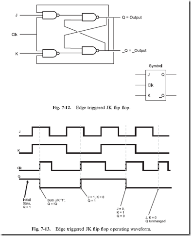
The most basic type of edge triggered flip flop is the ‘‘JK’’ (Fig. 7-12), which provides a similar function to the RS flip flop except that it changes state when the ‘‘clock’’ input is ‘‘rising’’ (changing from ‘‘0’’ to ‘‘1’’), as shown in the waveform diagram of Fig. 7-13.

There are a few points about Fig. 7-13 that should be discussed. I have assumed that in the initial state for this example, the output value ‘‘Q’’ is ‘‘1’’. When the first rising edge of the clock (‘‘Clk’’) is encountered, both J and K are 1, so Q ‘‘toggles’’ or changes state. Next, when the rising edge of the clock is encountered, J is 1 and K ¼ 0, so Q becomes 1 and the opposite is true for the next rising edge. In the final rising edge, both J and K are 0 and the value of Q remains the same. There is no metastable state for the JK flip flop. The operation of the JK flip flop is outlined in Table 7-4.

image

Just as a small circle on an input or an output of a logic gate indicates that the value is inverted, the clock pin on some chip diagrams is indicated by a small triangle. This convention helps minimize the clutter present in a logic diagram.

The JK flip flop is useful in general digital electronics applications, but it does not provide the necessary function for a computer register. Ideally,

image

a clocked register’s block diagram is quite simple (Fig. 7-14), consisting of a data line passed to the flip flop along with a ‘‘clock’’ line. While the data line stays constant, the contents of the flip flop doesn’t change. When the clock line goes from high to low, the data is stored in the flip flop – this is known as a ‘‘falling edge clocked flip flop’’ or a ‘‘falling edge clocked register’’ and it is probably the most common type of flip flop that you will work with.

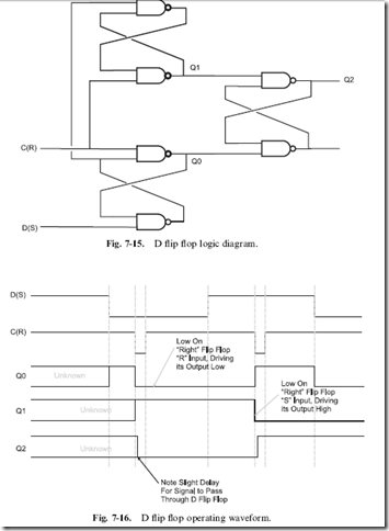
The edge triggered flip flop (Fig. 7-15) is based on the RS flip flop. Instead

of always calling this circuit a ‘‘falling edge triggered flip flop’’ or ‘‘clocked register’’, this circuit is normally known as a ‘‘D flip flop’’. The organization of the flip flops used in this circuit may seem complex, but their operation is actually quite simple: the two ‘‘input’’ flip flops ‘‘condition’’ the clock and data lines and only pass a changing signal when the clock is falling, as I show in Fig. 7-16. To try and make it easier for you to understand, I have marked the outputs of the RS flip flops in Fig. 7-15 and showed the waveforms at these points.

image

Note that in Fig. 7-16, I have marked the flip flop states before the first clock pulse as being ‘‘unknown’’ (in Fig. 7-14, the initial state was assumed). This is actually a very important point and one that you will have to keep in mind when you are designing your own circuits. You cannot expect a flip flop to be at a specific state unless it is set there by some kind of ‘‘reset’’ circuit (which is discussed in the next section). The output of the edge triggered flip flop stays ‘‘unknown’’ until some value is written in it. If you look at the signals being passed to the right flip flop (Output Q0), you will see that the inputs are unknown until the ‘‘data’’ line becomes low, at which point the two inputs to the right flip flop become high and the ‘‘unknown’’ bit value is stored properly in the flip flop.

The first value written into the D flip flop is ‘‘zero’’, the ‘‘data’’ line’s value for the write is changed before the ‘‘clock’’ line goes negative. When the ‘‘clock’’ line goes low, it forces out a ‘‘1’’ to be passed to the ‘‘right’’ flip flop, keeping it in its current state. The operation of the edge triggered flip flop should become very obvious if you were to build it (it would require two 74C00s).

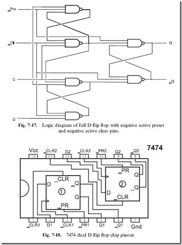
I find the D flip flop to be the flip flop that I build into my circuits most often. It is simple to work with and can interface to microcontrollers and microprocessors very easily. It is, however, quite awkward to wire, especially when you want to work with the ‘‘full circuit’’, which is shown in Fig. 7-17.

This circuit not only has data stored on the rising edge of the clock line but also two other lines ‘‘_Clr’’ and ‘‘_Pre’’ will force the flip flop’s output to a ‘‘0’’ (low voltage) or a ‘‘1’’ (high voltage), respectively, when they are pulled low. This allows for a number of different options for using the D flip flop in your circuit that can allow you to pull off some amazing feats of digital logic.

If you want to experiment with this circuit using two input NANDs (74C00s), I must warn you that it will be quite difficult and complex for you to wire. If you were to use three gates to produce one three input NAND gate, 18 NAND gates would be required to implement the full D flip flop function, which would require four and a half 7400 chips. To demonstrate the operation of the circuit, you could build it out of two 7410 (three, three input NAND gates) or be lazy like I am and just use one 74LS74 (Fig. 7-18) to experiment with the different functions of the full D flip flop.

The 7474 chip consists of two D flip flops with both the ‘‘Q’’ and ‘‘_Q’’ outputs passed to the chip pins. All four inputs shown in Fig. 7-18 (Data and Clock as well as two pins that provide you with the ability to set or reset the state of the flip flop without the use of the data or clock pins) are provided for each of the two flip flops built into the chip. The 7474 is a very versatile chip and can be used for a wide range of applications.

image


Feedback and Sequential Circuits :Latches Versus Registers and Reset

Latches Versus Registers

Two terms that are often used interchangeably are ‘‘register’’ and ‘‘latch’’. In the previous section, I introduced you to the ‘‘register’’, which is another

term for an edge triggered flip flop. When you look at parts lists and datasheets, you will see parts that are identified as ‘‘registers’’ and others as ‘‘latches’’ and these parts will have the same pinouts with no obvious differentiation in operation between the devices. Furthermore, I have found many chip manufacturers that have labeled their parts as ‘‘latches’’ when in fact they were ‘‘registers’’ and vice versa.

Quite simply put, ‘‘registers’’ are flip flops that store data when the rising (low to high or 0 to 1) or falling (high to low or 1 to 0) edge (whichever is used by the device) is received on the ‘‘clock’’ (or, my abbreviation, ‘‘Clk’’) pin. Registers are aptly named because they are normally used as simple data storage devices for microprocessor memory.

Latches are often used in microprocessor applications to save an address on a multi-purpose bus.

The best analogy for the ‘‘latch’’ that I can think of is a latch on a barn door: when the latch is not engaged, animals and whatever can wander in.

Once the latch is closed, what is in the barn stays in. The ‘‘latch’’ flip flop works similarly to this; with one state of the clock line, the input data is passed to the output directly and can be changed at any time (i.e. there isn’t any storage) but once the clock line changes state, the last value of the data is stored in the latch until the clock changes value.

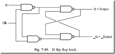
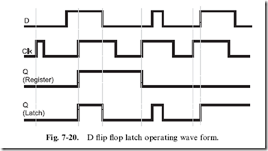
In the previous section, I introduced you to the edge triggered D flip flop ‘‘registers’’. The D flip flop ‘‘latch’’ is actually quite a bit simpler (Fig. 7-19), but what is interesting about it is that it doesn’t work anything like its edge triggered cousin. In Fig. 7-20, I have drawn a data input along with a clock and the ‘‘Q’’ (output pin) values for an edge-triggered D flip flop register and a D flip flop latch.

You will probably be surprised to see that waveforms for the two memory devices are completely different. The edge triggered D flip flop register clip_image086_thumbstores data in a very consistent and logical way – every time the clock pin

image


image

rises, the value of ‘‘D’’ is stored in the flip flop and nothing changes until the next rising edge of the clock pin.

The latch, on the other hand, seems to operate more like an AND gate than a memory storage device. The storage function tends to be obfuscated in the example of Fig. 7-20 because in many cases, I show the D pin changing state before the clock line returns low. This is an important point because many people consider the two devices to be interchangeable and this is simply not the case. Latches and registers have different applications and it is critical for you to understand what they are. You cannot put a latch chip in place of a register simply because they are pin compatible; you must make sure that the incoming data does not change state until the clock goes low.

Interestingly enough, latches do not need as much time to save data as a register; there are 9 fewer gate levels for a signal to pass through and even though I show the data save operations being instantaneous in Fig. 7-20, they are not. The latch can take as little as one-third of the time to save data as a register and only requires two gate delays before passing the data along (after which the data can be stored). This makes the latch an important chip for working with microprocessors with a ‘‘multiplexed’’ address bus.

Reset

If you cycle the power to any flip flop, you will have noticed that the initial ‘‘state’’ (or value) can be either ‘‘0’’ (LED off) or ‘‘1’’ (LED on), with no way of predicting which value it will be. This is normal because when power is applied to the flip flop it will start executing in the metastable state, and for any kind of imbalance in the circuit (e.g. residual charge or induced voltage) on the inputs of either NAND/NOR gate, the flip flop will respond and this will be its initial state. Often, this random initial state is not desired – instead, the circuitry should power up into a specific known state for it to work properly. This is why throughout this chapter I have taken pains to note that the initial state of a flip flop is not known. You may find that an application with one flip flop usually powers up the same way; if you were to do a statistical analysis of the power up values, you might even find that a single power up state approaches 100%, but you cannot guarantee this for all occurrences of the chip, or even that all other similar chips in the same application circuit will power up the same way.

Specifying the state when the circuit is powered up is known as ‘‘initialization’’ (just as it is for programming) and is required for more than just sequential logic circuits. Initialization normally takes place when the application is ‘‘reset’’, or waiting to start executing. To avoid confusion later, I should point out there are two types of ‘‘reset’’ described in this book when I talk about digital circuits. Earlier, when I was talking about simple combinatorial circuits, I also called a ‘‘low’’ or ‘‘0’’ voltage level ‘‘reset’’ (and ‘‘high’’ or ‘‘1’’ as ‘‘set’’). Now, when the term ‘‘reset’’ is used, I am describing the state when the circuit is first powered up or stopped to restart it from the beginning. When you read the term ‘‘reset’’ later in the book (as well as in other books), remember that if a single bit or pin is being described, the term ‘‘reset’’ means that it is ‘‘0’’ or at a low level. If a sequential circuit (like a microcontroller) is ‘‘held reset’’ or ‘‘powering up from reset’’, I mean that it is being allowed to execute from a known state.

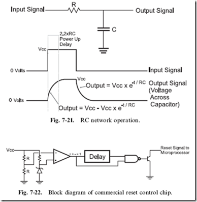
The ‘‘_CLR’’ pin on the full D flip flop (like the 7474) is known as a ‘‘negative active control’’ and is active when the input is at a ‘‘0’’ logic level. To make this pin active during power up, yet allow the chip to function normally, a resistor/capacitor network on the TTL input pin delays the rise of the pin (as shown in Fig. 7-21) so that the pin is active low while power is good. When the signal on ‘‘_CLR’’ goes high, and the clear function is no longer active, the chip can operate normally, with it being in an initial known state.

The time for the RC (resistor/capacitor) network to reach the threshold voltage can be approximated using the equation:

image

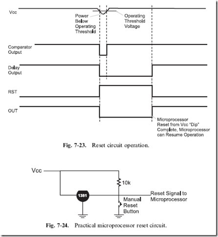
When you work with microprocessors and microcontrollers, you will want to implement a more sophisticated reset circuit. Many microprocessor manufacturers recommend an analog comparator based reset circuit like the one shown in Fig. 7-22. This circuit controls an open collector (or open drain)

image

transistor output pin that will pull down a negative active reset pin when power dips below some threshold value. This circuit is often available as a ‘‘processor reset control’’ chip and is put into the same black plastic package as a small transistor (known as a TO-92).

Processor reset control chips are available for a very wide variety of different ‘‘cut off ’’ voltages, ranging from 2.2 volts and upwards. Figure 7-23 shows the operation of the internal parts of the processor reset control chip when the input voltage drops below the set value; the comparator stops outputting a ‘‘1’’ and a delay line is activated. This delay line is used to filter out any subsequent ‘‘glitches’’ in the power line and makes sure that the power line is stable before allowing the processor to return from reset and continue executing. When the comparator outputs a low value or the delay line is continuing to output a low value, the output of the NAND gate they are connected to is high and it turns on the open collector output transistor, pulling the circuit to ground.

The Panasonic MN1381 line of chips is a very popular processor reset control and can be used to control a sequential circuits reset using

image

a circuit similar to the one shown in Fig. 7-24. This circuit will take advantage of the RC network delaying the rise of the control signal, provide you with the ability to reset or stop the operation of the micro- processor and halt the operation of the robot if the battery falls below a safe minimum.

If you power on and off a circuit quickly, you may find that it does not power up properly. This is due to the capacitor in the reset circuit not discharging fully – it may take as much as 10 seconds for it to discharge completely. This was actually an issue with the original IBM PC; if you had a situation where the PC ‘‘hung’’, you would have to power down and wait at least 15 seconds to make sure that the reset circuit would allow the computer to power up properly.

Quiz

1. Feedback in digital electronics:

(a) Is built into every gate

(b) Must always be avoided

(c) Can be used to store bit data

(d) Is only used in radio interface circuitry

2. Ring oscillators can be used:

(a) In digital watches

(b) To measure the gate delay of a logic technology

(c) To test the operation of a combinatorial circuit

(d) Only when current limiting resistors are in place to protect gate outputs

3. What do the letters ‘‘R’’ and ‘‘S’’ stand for in the RS flip flop?

(a) ‘‘Recessive’’ and ‘‘Static’’

(b) ‘‘Reset’’ and ‘‘Set’’

(c) ‘‘Rothchild’’ and ‘‘Stanislav’’

(d) ‘‘Receive’’ and ‘‘Send’’

4. What is the ‘‘metastable state’’ of a flip flop?

(a) When it has started to oscillate

(b) The time between when the inputs change the output is correct

(c) The state in which the outputs of a flip flop are half way between ‘‘0’’ and ‘‘1’’ and can be easily ‘‘pushed’’ into a specific state

(d) The state in which ‘‘Q0’’ is unknown

5. ‘‘Toggling’’ a bit means:

(a) Setting (making the output a 1) of a bit

(b) Leaving the bit in its current state

(c) Inverting the bit’s state

(d) Resetting (making the output a 0) of a bit

6. A ‘‘Register’’ can be used in:

(a) Nowhere, it is a thought experiment used to show feedback in a digital application

(b) Just computer processors

(c) Just sequential digital electronics application

(d) Just about any digital electronics application

7. The ‘‘_Pre’’ pin of a D flip flop will:

(a) Set the bit

(b) Reset the bit

(c) Nothing

(d) Toggle the state of the bit

8. Which formula specifies the RC network response to a sudden voltage input?

image

9. Why are latches like barn doors?

(a) They provide a secure environment for what’s inside them

(b) They are both relatively heavy

(c) They allow free passage until the latch is engaged

(d) They are the fastest method for passing things in and out

10. Which application is a latch best suited for?

(a) Main memory in a computer system

(b) Bicycle lock combinations

(c) Stopping and saving data mid-stream

(d) Temporary storage of data in a microprocessor


Practical Combinatorial Circuit Implementation : Quick and Dirty Logic Gates ,Dotted AND and Tri-State Logic , Drivers and Combining Functions on a Net

Quick and Dirty Logic Gates

One of the most frustrating aspects of designing digital electronic circuits is that when you are almost finished, you often discover that you are a gate or two short and you are left with the question of whether or not you should add another chip to the circuit. The major problem with adding another chip to the circuit is the requirement for additional space to place the chip in the circuit. Along with the need for additional space, adding another chip will add to the costs of the application and the difficulty in assembling it. In Chapter 2, I discussed that by using the Boolean arithmetic laws and rules, you could produce various functions using different gates than the ones that are ‘‘best suited’’ for the requirements. In the cases where there are no leftover gates available, a gate can be ‘‘cobbled’’ together with a few resistors, diodes and maybe a transistor. These simple gates are often referred to as being ‘‘MML’’ or ‘‘Mickey Mouse logic’’ technology because they can generally be used in most situations and with different logic families when a quick and dirty solution is required.

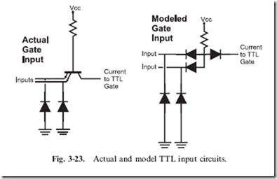
To be used successfully, they must be matched to the inputs and outputs of the different logic families that you are using and should not result in long switching times, which will affect the operation of the application, or large current draws, which could damage other components. As a rule of thumb, do not use one of the simple gates presented here between differing

image

technology gates; you will find that operation of different technologies can often be incompatible when you are adding resistors, diodes and transistors like the ones used in the sample gates presented here. Another rule of thumb is to make sure that each MML gate only drives one input – you can get into trouble with input fan-outs and multiple gate current sinking requirements very quickly. Along with trying to satisfy these requirements, there are cases where you will find that the MML gate will require at least as many pins as adding another chip and will be more difficult to wire. Generally speaking, adding MML gates to your application should be considered a ‘‘last’’ resort, not something you design in right from the start.

The most basic MML gate is the ‘‘inverter’’ and should not be a surprise.

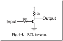
Figure 6-4 shows the circuit for the MML inverter, built out of two 10 k resistors and an NPN transistor. This inverter is actually a basic ‘‘RTL’’ (resistor–transistor logic) technology device and outputs a high voltage, when it is not being driven by any current. When current is passed to the gate, the transistor turns on and the output is pulled to ground (with good current sinking capability).

This circuit (as well as the other MML gates I discuss in this section) cannot handle high voltage or current inputs and outputs as well as commercially available logic gates and need to be ‘‘buffered’’. The need for buffering the MML’s gate inputs and output is an important point to note when considering using an MML gate in an application. As a rule, MML gates must be placed in the middle of a logic ‘‘string’’ rather than at the input or output ends to ensure that if you are expecting certain characteristics (such as the ability to drive a LED), standard TTL or CMOS technology gates will provide you with it.

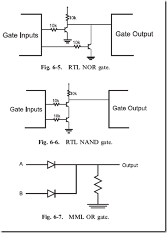
The inverter circuit can be simply modified by adding another transistor and resistor, as shown in Fig. 6-5, to create an RTL NOR gate. The RTL NAND gate is shown in Fig. 6-6. The NOR gate is considered the basis of RTL technology.

Implementing an AND or OR gate in MML is a bit more complex and requires a good understanding of the input/output parameters

image

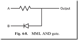
of the logic families. In Fig. 6-7, I have shown a sample design for an OR using two diodes and a resistor. The use of a 470 ohm resistor is probably surprising, but it was chosen to allow the gate to be used with both CMOS and TTL logic. In this case, if neither input has a high voltage, then the output will pull the input to ground. If the input is a CMOS gate, then the input will behave as if it were tied to ground. The 470 ohm resistor will allow the TTL input current to pass through ground and it will behave as if the input was at a low logic level. When the resistor is connected to a CMOS input, it will be effectively tying the input to ground, even though no current is flowing through it. In either case, when one of the inputs is driven high, the input pin will be held high and the gate connected to the output of the OR gate will behave as if a high logic level was applied to it.

An MML AND gate (Fig. 6-8) is the simplest in terms of the number of components. The diode and resistor work together to provide a high voltage

image

when both inputs are high, but when one of them is pulled low, the voltage level will be pulled down and current drawn from the input gate it is connected to.

While the MML AND presented in Fig. 6-8 will work in virtually any application, you may find that you will want to use a 470 ohm resistor in the circuit and a 10 k one in CMOS logic applications. The reason for doing this is to minimize the current drawn by the application; with a 470 ohm resistor, roughly 10 mA will be drawn when the output of the gate is low. This current draw decreases to 100 mA when a 10 k resistor is used instead for the resistors in these two gates.

Dotted AND and Tri-State Logic Drivers

You may feel constrained by the rule that you can only have one driver on a single line (or net). In Chapter 3, I introduced you to the concept of the ‘‘dotted AND’’ bus in which there was a common pull up on the net along with a number of transistor switches, each one of which could ‘‘pull’’ the net to a low voltage/logic level (and draw the current from any TTL gates inputs connected to the dotted AND). The dotted AND works reasonably well and has the advantage that it can control output voltages greater than the power applied to the logic chips. Some more subtle advantages are that more than one output can be active (tying the net to ground) and the operation of the bus will not be affected and TTL open collector and CMOS logic open drain outputs can be placed on the bus along with mechanical switches and other devices which can pull the bus to ground.

The dotted AND bus’s main disadvantage is its inability to source significant amounts of current. Smaller value pull up resistors can be used, but this increases the amount of current passed to ground when one of the open collector transistors is on. The dotted AND can be considered to be quite inefficient if it is low for a long period of time, because it is passing current directly to ground. The inability to source large amounts of current

image

is a drawback when high-speed signals are involved is the major disadvantage of the dotted AND bus. Changing an input from a high to a low, especially when there are some relatively large capacitances on the net, the switching time can become unreasonably slow.

A common error made by new circuit designers when they are adding a dotted AND bus to their designs is forgetting to add the pull up resistor. If the resistor has been forgotten, then the bus will never have a ‘‘high’’ voltage (although it will have a ‘‘low’’ voltage that can be detected). You will find that TTL inputs connected to a dotted AND but not having a pull up will work correctly, but CMOS logic inputs will not.

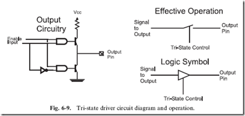
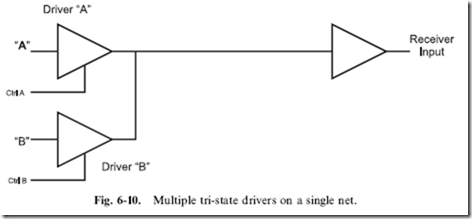
Another solution to the problem of wanting to have multiple drivers on the same net is to use ‘‘tri-state’’ drivers (Fig. 6-9). These drivers can ‘‘turn off’’ the transistors as effectively as if a switch were opened (the diagram marked ‘‘Effective Operation’’ in Fig. 6-9).

The left-hand side of circuit diagram of Fig. 6-9 shows how the tri-state driver works. If the tri-state control bit is inactive, the outputs of the two AND gates will always be low and the NPN output transistors can never be turned on. This ‘‘inactive’’ state is also known as the ‘‘high impedance state’’. When the tri-state control bit is active, then a high to either the top or bottom NPN transistor will allow the output to behave as an ordinary TTL output.

This ability to ‘‘turn off’’ allows multiple drivers, such as I have shown in Fig. 6-10, to be wired together. In this case, if data was to be placed on the net from Driver ‘‘B’’, the ‘‘Ctrl A’’ line would become inactive (the ‘‘high impedance state’’), followed by the ‘‘Ctrl B’’ line becoming active. At this point, the bus would be driven with the data coming from Driver ‘‘B’’.

image

It is important that only one tri-state driver is active at one time because the voltage on the common net will be indeterminate, as will be the logic level. You may be thinking that the term ‘‘indeterminate’’ to be the case when two drivers are active and are attempting to drive the net at different levels. This is true, but it is often also the case if two different drivers are driving at the same level: CMOS logic and TTL drivers will attempt to drive the net to different voltage levels and even TTL will not give repeating answers when you are trying to understand what is happening. The technical term for the situation where two tri-state drivers are active at the same time is ‘‘bus contention’’ and it should be avoided at all costs – only one driver should be active on the net at any one time.

At the start of this section, I noted that there could be more than one output active on a net at the same time. Note that when I say ‘‘multiple active outputs’’, I mean more than one driver pulling the net low. I do not recommend this to be part of the design, however; multiple active outputs are impossible to differentiate and you will have problems figuring out which bits are active and what signal is being sent (with multiple outputs active, state changes from one output will most likely be masked by the active operation of others).

Before leaving this section, I do want to point out that tri-state drivers can be used on a dotted AND bus. This is probably surprising, considering the dire warnings I have put in regarding bus contention. The trick to adding a tri-state driver to a dotted AND bus is that it is normally disabled and only a low voltage can be put on the net by the tri-state driver. High values are output by simply disabling the tri-state driver and letting the net’s pull up provide the high voltage. Combining Functions on a Net

As a purely intellectual exercise, it can be interesting to see how many functions you can build into a single digital electronics net. From a practical point of view, cramming multiple functions on a single line will minimize the amount of effort that must be expended to build a prototype application. Many products carry out multiple functions on a single line; generally, this is done to allow the manufacture and sale of simpler products. Whatever the motivation, ‘‘stretching’’ a logic technology to allow multiple functions on a single net requires a strong knowledge of the technology’s electrical parameters and the technology’s normal operating conditions. The most important thing to remember is that the input/output devices attached to the net must be properly coordinated to make sure that data is read and written at the right times.

The most obvious ways of connecting two drivers together is to use dotted AND and tri-state drivers on a ‘‘bus’’, as I discussed in the previous section.

These methods work well and should be considered as the primary method of implementing multiple devices on the net. The other methods discussed here work best for specific situations; but there is no reason why you can’t modify your design to take advantage of these specific instances.

When interfacing the bi-directional digital I/O pin to a CMOS driver and a CMOS receiver (such as a memory with separate output and input pins), a resistor can be used to avoid bus contention at any of the pins, as is shown in Fig. 6-11. Using this wiring, when the bi-directional I/O pin is driving an output, it will be driving the ‘‘Data In’’ pin register, regardless of the output of the ‘‘Data Out’’ pin. If the bi-directional and ‘‘Data Out’’ pins are driving different logic levels, the resistor will limit the current flowing between the bi-directional and the memory ‘‘Data Out’’ pin. The value received on the ‘‘Data In’’ pin will be the bi-directional device’s output.

When the bi-directional digital I/O is receiving data from the memory, clip_image035_thumbthe I/O pin will be put in ‘‘input’’ (or ‘‘high impedance’’) mode and the

image

image

‘‘Data Out’’ pin will drive its value to not only the bi-directional device’s I/O pin, but the ‘‘Data In’’ pin, as I noted above. In this situation, the ‘‘Data In’’ pin should not be latching any data in; the simplest way to ensure this is to make the digital I/O pin part of the I/O control circuitry. This is an important point because it defines how this circuit works. A common use for this method of connection data in and data out pins is used in memory chips that have separate data input and output pins.

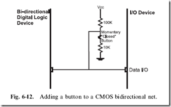
User buttons can be placed on the same net as logic signals as Fig. 6-12 shows.

When the button is open or closed, the bi-directional logic device can drive data to the input device, the 100 k and 10 k resistors will limit the current flow between Vcc and ground. If the bi-directional logic device is going to read the button ‘‘high’’ (switch open) or ‘‘low’’ (switch closed) it will be driven on the bus at low currents when the pin is in ‘‘Input Mode’’. If the button switch is open, then the 100 k resistor acts like a ‘‘pull up’’ and a ‘‘1’’ is returned. When the button switch is closed, there will be approximately a half volt across the 10 k resistor, which will be read as a ‘‘0’’.

The button with the two resistors tying the circuit to power and ground is

like a low-current driver and the voltage produced is easily ‘‘overpowered’’ by active drivers. Like the first method, the external input device cannot receive data except when the bi-directional device is driving the circuit. A separate clock or enable should be used to ensure that input data is received when the bi-directional device is driving the line.

This method of adding a button to a net can be extrapolated to work with a switch matrix keyboard (presented later in the book), although the circuit and interface operation will become quite complex. Secondly, a resistor/ capacitor network for ‘‘debouncing’’ the button cannot be used with this circuit as it will ‘‘slow down’’ the response of the bi-directional device driving

the data input pin and will cause problems with the correct value being accepted.

For both of these methods of providing multiple features to a single net, you should only use CMOS logic as it is voltage controlled and not current controlled, like TTL. You may be able to use TTL drivers with these circuits, but they may be unreliable. To avoid problems with invalid currents being available to TTL receivers, just use the latter two circuits with CMOS digital logic.

Designing a circuit in which multiple functions are provided on a single net

for an application is not always possible or even desirable. Like any design feature implemented in an application, before trying to combine multiple functions on a single net, you should understand the benefits as well as the costs. When it is possible, you can see some pretty spectacular results; my personal record was for a LCD driver in which I was able to combine five functions on a single net – LCD Data Write, LCD Data Read, Data In Strobe, Data Ready Poll and configuration switch poll.

Quiz

1. What parameter is not listed in the chip characteristic card?

(a) Input fanout

(b) Number of gates built into the chip

(c) Electrical dependencies

(d) Maximum operating speed

2. What is not a typical digital electronic output pin type?

(a) Totem pole

(b) Open collector

(c) High-current

(d) Tri-state driver

3. Other than the XOR gate, are any other of the six basic I/O gates capable of producing race conditions just by themselves?

(a) Each one is capable of producing a race condition under certain circumstances

(b) The NOR Gate in TTL

(c) The AND Gate in CMOS Logic

(d) No

4. What is not a factor in determining if a marginal circuit and component will produce a race condition?

(a) Ambient temperature

(b) Net length

(c) Power voltage

(d) The phases of the moon

5. Mickey Mouse logic should be used:

(a) Never

(b) When you are in a hurry to get the application finished

(c) When you have board space, cost and available gate constraints that preclude adding a standard chip

(d) When there is a need to pass a CMOS output to a TTL input

6. Each item is an advantage of a dotted AND bus except:

(a) The dotted AND bus can have tri-state drivers on it as well as mechanical switches

(b) The dotted AND bus can control voltages greater than the chip’s Vdd/Vss

(c) The dotted AND bus is cheaper than one manufactured with tri-state drivers

(d) The dotted AND bus can consist of CMOS logic as well as TTL drivers

7. When tri-state drivers are inactive, another term that is used to describe the state is:

(a) High resistance

(b) High impedance

(c) Low current output

(d) Driver isolation

8. When should multiple tri-state drivers be active?

(a) When more current is required on the net

(b) When more speed is required on the net

(c) When the receiver detects an ambiguous logic level

(d) Never

9. When adding a push button to a net, can the 100 k resistor connected to positive power and the 10 k resistor connected to positive power be swapped?

(a) Yes

(b) No

(c) Only if TTL receivers and drivers are used.

(d) Yes, if you can ensure that the signals passing between the digital devices are still within specified operating margins.

10. When putting a receiver and driver on the same net, can the current limiting resistor be wired between the bi-directional logic device and the ‘‘Data In’’ pin, leaving a direct connection between the bi-directional logic device and ‘‘Data Out’’?

(a) Yes. There aren’t any cases where it wouldn’t work

(b) Yes, if the resistor value is within 1 k and 10 k

(c) Yes, for certain technologies of CMOS logic

(d) No. This will cause bus contention


Practical Combinatorial Circuit Implementation: Race Conditions and Timing Analysis

Practical Combinatorial Circuit Implementation

When you are designing your first application that is built from digital electronics, you will probably feel like you have just joined a never-ending role-playing game in which all the other players know more than you do. Later in the book, I will present some ideas on how to read a datasheet and what to look for in it, but for now, I would like to discuss a number of the options that you should be aware of and are thinking about when you first start designing your application.

Using the role-playing game analogy with digital electronics may seem to be facetious, but there are actually a lot of similarities that you should be aware of. First and foremost, each digital electronic chip that you can choose from has a number of characteristics that you will have to be aware of and

Table 6-1 Important characteristics of a digital electronic chip.

Characteristic

Comments

Function

Gate type, chip function

# Bits

The number of bits per gate input or number of bits used by the function

# Gates/functions

What does the chip do and how many are there

Technology

Electronic standard chip is implemented

Output type

Gate output type

Dependencies

Issues to be aware of

Manufacturer

Who makes the chip/where can it be purchased

choose from when you are specifying the parts used in your application. When choosing between the parts, it might be a good idea to come up with a card, similar to the cards used in role-playing games to explain the different characters, characteristics and strengths and weaknesses. A sample card for a digital electronic device might look something like Table 6-1.

The ‘‘function’’ of the chip is a brief description of the gates provided by the chip or the digital logic function provided by the chip (such as an adder or a magnitude comparator). At this point in the book, you might feel that it is sufficient to specify a chip for a needed function, but the following characteristics are critical for you to understand that you need to be able to select the right chip for the right application.

When I have presented simple gates, they have all (with the exception of the NOT gate) two inputs. Along with two inputs, there are a number of different inputs for a variety of different types of gates. For example, in standard TTL, you can get NAND gates with two, three, four and eight inputs. Four and eight bit adders as well as different chips with different bit counts are also available. When selecting a chip for an application, you should be cognizant of the bit options that are available to minimize the number of chips required.

The basic TTL chips have four two input gates and six one input gates, but if the number of bits changes, then the number of gates within the chip changes (or the plastic package type and the number of pins changes). As surprising as it seems, many complex functions can have more than one built into the package. Like the number of bits, the number of functions within the chip will help you plan out how many chips you will need in the application.

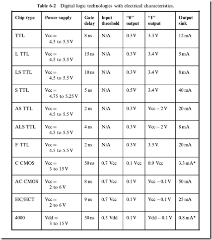
So far in the book, I have really just indicated that there are two types of technology used for standard logic devices. In actuality, there are dozens and in Table 6-2, I have listed the most popular ones with their input, output and operating characteristics. For the different varieties of ‘‘TTL’’, ‘‘C’’, ‘‘AC’’

image

and ‘‘HC/HCT’’ logic families, the part number starts with ‘‘74’’ and for the ‘‘4000’’ series of CMOS chips, it has a four digit part number, starting with ‘‘4’’. Table 6-2 lists the different aspects of the different types of logic chips that you will want to work with.

The ‘‘output sink’’ currents are specified for a power voltage of 5 volts. If you increase the power supply voltage of the indicated (with a ‘‘*’’) CMOS parts, you will also increase their output current source and sink capabilities considerably.

In Table 6-2, I marked TTL input threshold voltage as ‘‘not applicable’’ (N/A) because, as you know, TTL is current driven rather than voltage driven. You should assume that the current drawn from the TTL ,input is 1 mA for a ‘‘0’’ or ‘‘low’’ input. CMOS logic is voltage driven, so the input voltage threshold specification is an appropriate parameter.

The output current source capability is not specified because many early chips were just able to sink current. This was all that was required for TTL and it allowed external devices, such as LEDs, to be driven from the logic gate’s output without any additional hardware and it simplified the design of the first MOSFET-based logic chips. The asterisk (‘‘*’’) indicates that the sink current specification is for 5 volts power; changing the power supply voltage will change the maximum current sink capability as well.

There are three basic output types: totem pole, open collector and the tri-state driver (which is presented later in this chapter). In cases where multiple outputs are combined, different output types should never be combined due to possible bus contention.

Virtually all of the electrical dependencies that you should be aware of are listed in Table 6-2, but you may have a number of operating dependencies (such as making sure CMOS inputs are tied high or low) or physical design issues that you should be aware of. ‘‘Physical design’’ is the process of designing a printed circuit board with internal connections built into it that have the chips soldered onto it. The primary chip dependencies that you should be aware of when designing a printed circuit board are the location and type of the chip’s pins as well as any heat removal (i.e. heat sinks) requirements that the chip may have.

Finally, you should know who makes the part and where you can purchase it. This point is often overlooked, but you will find many manufacturers that advertise parts that are seemingly designed just for your application. The first problem that you encounter is that your company has a policy of only buying parts that are available from multiple sources or you may discover that the manufacturer is not considered to be reliable and production quantity parts are difficult to come by. For your first designs, it is a good rule to only use parts that are easily obtainable and, ideally, built by multiple sources.

This may make the design operation a bit more difficult and the final product larger than it could have been, but chances are the product will go through manufacturing very smoothly and with few difficult ‘‘hiccups’’.

Race Conditions and Timing Analysis

As you begin to create digital electronic circuits that are more and more complex and run faster and faster, you are going to discover that they are going to stop working or they are going to start working unpredictably. In trying to find the problem, you will probably look at different parts of the circuit, ranging from the power supply to the wiring and maybe rebuilding it several times to see if it is being affected by other electrical devices running near the application. At some point you will give up and build as well as redesign the circuit, only to discover that the problem is still there.

So what’s the problem? Chances are you have encountered a ‘‘race condition’’, which is normally defined as ‘‘A condition in digital electronics where two or more signals do not always arrive in the same order.’’ Personally, I use a slightly different definition for race condition which states that ‘‘A race condition occurs in any digital electronic circuit where the output to input response time changes according to the inputs passed to it.’’ My definition is a bit more specific and should give you some ideas on where to look for the problem.

Simply put, a race condition is a case where an expected event does not occur.

To illustrate the issue, assume that the application consists of a circuit that is designed to respond to an internal value at a specific time. If the digital electronics used to produce this internal value does not always complete within the specified time, what happens in the circuit that uses this value for input? Chances are the circuit will respond incorrectly, resulting in the problem that you are trying to debug.

An example circuit that has the capability of producing a race condition is shown in Fig. 6-1.

image

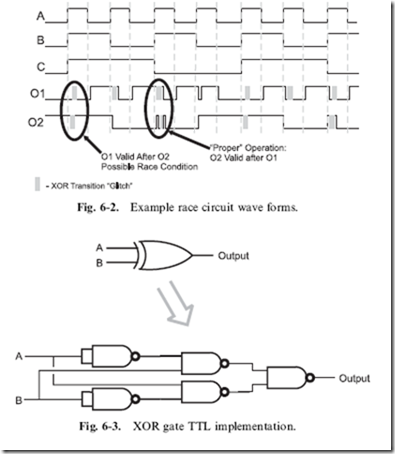
Figure 6-2 is the waveform output of this circuit to a three bit incrementing signal and, in it, I have indicated the output bits (‘‘O1’’ and ‘‘O2’’) and indicated where the operation of the circuit is ‘‘correct’’ (O2 is valid after O1) as well as a possible race condition (when O1 is valid after O2). I have also indicated times, using a shaded block, when both of the XOR inputs are changing and there could be a ‘‘glitch’’ caused by both inputs changing state simultaneously, at which time the output of the XOR gate is unknown.

The glitch produced by the XOR gate is an excellent example of a race condition. As I presented earlier in the book, the XOR gate is typically made up of five NAND gates in the configuration shown in Fig. 6-3. If one input changes, then the output will change state to either ‘‘1’’ or ‘‘0’’ without any glitches, but what happens when the two inputs change state simultaneously?

Quickly thinking about it, you might think that the output doesn’t change state, but consider what happens at the NAND gate level of the XOR gate.

image

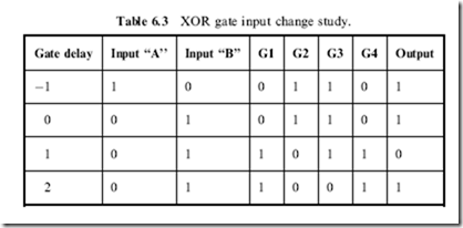
imageTable 6-3 lists the NAND gate outputs for the different gates as I’ve marked them in Fig. 6-3. To help illustrate what’s happening, I use ‘‘gate delays’’ as the time increments of this study. In Table 6-3, the initial conditions are one gate delay before the two inputs change value. The inputs change value at gate delay ‘‘0’’.

According to this study, at gate delay 1, the output will be a ‘‘0’’ because

the direct inputs from A and B to G3 and G4 have changed at gate delay 0, but the inverted inputs from G1 and G2 have not. It won’t be until gate delay 2 that the inputs to NAND gates G3 and G4 have stabilized. Thus, the time

from gate delay 1 to gate delay 2 will result in generally unknown logic levels, which are normally characterized by the term ‘‘glitch’’.

Going back to Fig. 6-2, you can probably observe what I mean by the race condition, but I’m sure it seems very subtle. Actually, this is the point that I want to make: race conditions are very subtle and are very difficult to observe. For this section, I spent quite a bit of time with a 74C85 (quad XOR gate), a PIC16F627A (Microchip PIC Microcontroller to produce the ‘‘A’’, ‘‘B’’ and ‘‘C’’ inputs to the circuit) and an oscilloscope trying to capture the events shown in Fig. 6-2. I gave up after about 5 hours of trying to capture the event on the oscilloscope in a way that it would be easily seen.

Race conditions are dependent on part mix, applied voltage and ambient conditions. You may find some sample circuits which never have the problem while others will never seem to work right. Finding the actual event is extremely difficult and only after doing a thorough timing analysis of the circuit will you find the opportunity for a race condition to occur. The prevention for this problem is quite simple – figure out what your worst case gate delay is through the circuit and only sample data after this time

(even add a 10% margin to make sure there is no chance of marginal components causing problems).

Avoiding the opportunity is why chip designers work at making sure multiple outputs are active at the same time for changing inputs. Looking at the ‘‘A’’/‘‘B’’/‘‘C’’ waveform of Fig. 6-2, you might have thought that it is impossible to achieve the signals at precisely the same time, but it is very likely that if a single gate is producing incrementing outputs, the ‘‘edge’’ of each output bit will be precisely aligned with each other and will cause the glitch on the output of the XOR gate.

The process of determining what is the worst case gate delay is the same process I used for finding the ‘‘glitch’’ in the XOR gate and is known as ‘‘timing analysis’’. It is unusual for somebody to work through this analysis by hand as I have done, except for very simple circuits. When timing analysis is done on a commercial product, it is normally done using a logic simulator, which can find the longest delays and report on any problems.


Binary Arithmetic Using Digital Electronics : Subtraction and Negative Numbers,Magnitude Comparators and Bus,Nomenclature and Multiplication and Division

Subtraction and Negative Numbers

As you might expect, binary subtraction has many of the same issues as addition, along with a few complexities that can make it harder to work with. In this section, I will introduce some of the issues in implementing a practical ‘‘subtracter’’ as well as look at some ways in which subtraction can be implemented easily with an existing addition circuit.

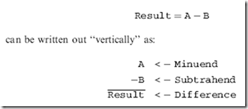
To make sure we’re talking the same language, I want to define the terms that I will be using to describe the different parts of the subtraction operation. The ‘‘horizontal’’ arithmetic equation:

image

The ‘‘minuend’’ and ‘‘subtrahend’’ terms are probably something that you forgot that you learned from grade school. I use them here because they are less awkward than referring to them as the ‘‘value to be subtracted from’’ and the ‘‘value subtracted’’. The term ‘‘difference’’ as being the result of a subtraction operation is generally well understood and accepted.

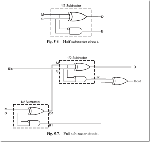
When you carry out subtraction operations, you do it in a manner that is very similar to how you carry out addition; each digit is done individually and if the digit result is less than zero, the base value is ‘‘borrowed’’ from the next significant digit. With the assumption that subtraction works the same way as addition, you could create a ‘‘half subtracter’’, which is analogous to the half adder and could be defined by the truth table shown in Table 5-5

The ‘‘difference’’ bit is simply the minuend and subtrahend XORed together, while the ‘‘borrow’’ bit (decrementing the next significant digit) is only true if the minuend is 0 and the subtrahend is 1. The borrow bit can be defined as the inverted minuend ANDed with the subtrahend. The equations

Table 5-5 ‘‘Half subtracter’’ defining truth table.

Minuend

Subtrahend

Difference

Borrow

0

0

0

0

0

1

1

1

1

1

0

0

1

0

1

0


image

for the half subtracter are listed below and the subtracter building block is shown in Fig. 5-6.

imageThe small circle on the single input indicates that the value is inverted before being passed into the gate. This convention avoids the need for putting a full inverter symbol in the wiring diagram of a digital circuit and is often used in chip datasheets to indicate inverted inputs to complex internal functions.

Two half subtracters can be combined into a ‘‘full subtracter’’, just as two half adders can be combined to form a full adder (Fig. 5-7). In Fig. 5-7, I have labeled the two half subtracters, so that their operation can be listed in Table 5-6, to test the operation of the full subtracter.

Table 5-6 Full subtracter operation truth table.

Bin

Minuend (‘‘M’’)

Subtrahend (‘‘S’’)

D1

B1

D

B2

Bout

0

0

0

0

0

0

0

0

0

0

1

1

1

1

0

1

0

1

1

0

0

0

0

0

0

1

0

1

0

1

0

0

1

1

0

1

0

0

0

0

1

1

1

0

0

1

1

1

1

0

1

1

1

0

0

1

1

0

0

0

0

1

1

1

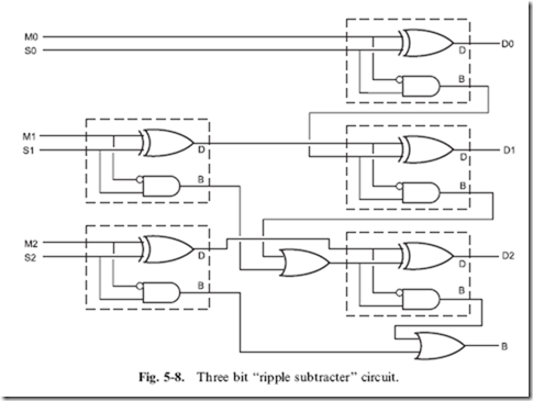
Like the ripple adder, full subtracters can be chained together to create a multi-bit subtracter circuit (Fig. 5-8) and a ‘‘borrow look-ahead’’ (to coin a phrase) subtracter could be designed, but instead of going through the pain of designing one, there is another option and that is to add the negative of the subtrahend to the minuend.

In the introduction to this chapter, I introduced the idea of negative

numbers as being the value being subtracted from an arbitrary large number and showed an example that produced ‘‘-5’’ in a universe where infinity was equal to one million. When you first went through this example, you might have thought that this was an interesting mathematical diversion and an illustration as to how negative and positive numbers converge when they approach infinity. This concept, while seemingly having little application in the ‘‘real world’’, is very useful in the digital domain.

In the digital domain, the term ‘‘infinity’’ can be replaced with ‘‘word size’’ and if the most significant bit of the word is considered to be the ‘‘sign’’ bit, positive and negative numbers can be expressed easily. In Table 5-7, I have listed the decimal, hex as well as the positive and negative values which take into account that a negative number can be written as:

imageThis negative value is known as a ‘‘two’s complement’’ negative number and is the most commonly used negative bit format used. There is a ‘‘one’s

image

complement’’ number format, but it does not avail itself as efficiently as two’s complement to allow for easier subtraction and addition of negative numbers.

Looking at the formula above, you are probably confused as to why it would be used because it requires both a subtraction operation as well as an addition operation to carry out one subtraction operation. Negating a number in two’s complement format does not actually require a subtraction operation; it can be done by inverting each bit (XORing each bit with 1) and then incrementing the result. Using the values of Table 5-7, you can demonstrate how a positive value is negated.

For example, to negate the value ‘‘5’’, the following steps are used:

1. Each bit of the number is XORed with ‘‘1’’. B’0101’ becomes B’1010’.

2. The XORed result is incremented. B’1010’ becomes B’1011’, which is ‘‘-5’’.

The opposite is also true: the individual bits can be inverted and the result incremented to convert a negative two’s complement value to a positive.

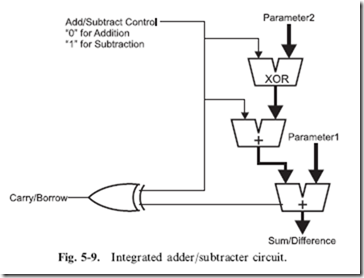
Once the value has been negated, it can be simply added to the other parameter, as I show in Fig. 5-9. There are three things that you should be

Table 5-7 Different ways of representing a four bit number.

Binary value

Decimal value

Hex value

Two’s complement value

B’0000’

0

0x00

0

B’0001’

1

0x01

1

B’0010’

2

0x02

2

B’0011’

3

0x03

3

B’0100’

4

0x04

4

B’0101’

5

0x05

5

B’0110’

6

0x06

6

B’0111’

7

0x07

7

B’1000’

8

0x08

-8

B’1001’

9

0x09

-7

B’1010’

10

0x0A

-6

B’1011’

11

0x0B

-5

B’1100’

12

0x0C

-4

B’1101’

13

0x0D

-3

B’1110’

14

0x0E

-2

B’1111’

15

0x0F

-1

aware of before leaving this section. The first is the use of the ‘‘V’’ shaped mathematical function symbols in Fig. 5-9; these symbols indicate that two parameters are brought together to form one output. I use this symbol when a group of bits (not just one) are passing through the same operation.

You might be wondering why instead of simply inverting the individual bits of the value to be converted to a negative two’s complement value, I XOR the bits with the value 1. The reason for doing this is in the interests

image

of practicality and looking ahead. In Fig. 5-9, I show a circuit in which two parameters can be added together or one can be subtracted by the other – the ‘‘switch’’ control for which operation is selected. If a 1 is passed to the ‘‘Parameter2’’ circuitry, each bit of Parameter2 is XORed with 1, inverting each bit and a 1 is passed to the Parameter2 adder, which increments the value. If a zero is passed to the Parameter2 circuitry, the bits of Parameter2 are not inverted and zero is added to the output of the XOR function, resulting in an unchanged value of Parameter2 being passed to the adder with Parameter1. To net it out, if a ‘‘1’’ is passed to this circuit, Parameter2 is subtracted from Parameter1; if a ‘‘0’’ is passed to the circuit, the two parameters are added together.

The last point to note is that the ‘‘carry’’ output of the final adder is a negated ‘‘borrow’’ output when the subtraction operation is taking place. To integrate the operation of the ‘‘carry/borrow’’ bit with the add/subtract switch bit, this bit is set when a carry or borrow of the next significant word is required, regardless of the operation.

Magnitude Comparators and Bus Nomenclature

Along with being able to add and subtract binary values, you will find the need to compare binary values to determine whether or not a value is less

than, equal to or greater than another value. Just as if this were a programming requirement, to test two binary values together, you would subtract one from the other and look at the results. An important issue when comparing a value made up of multiple bits is specifying how it is to be represented in logic drawings and schematic diagrams. In the previous section I touched on both these issues, in this section, I want to expand upon them and help you to understand a bit more about them.

When you are comparing two binary values, you are comparing the magnitude of the values, which is where the term ‘‘magnitude comparator’’ comes from. The typical magnitude comparator consists of two subtracters which either subtract one value from another and vice versa or subtract one value from another and then compare the result to zero. In either case, the magnitude comparator outputs values indicating which value is greater than the other or if they are equal.

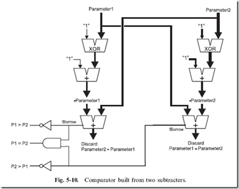
Figure 5.10 shows a basic comparator, which consists of two subtracters utilizing the negative addition discussed in the previous section. The differences are discarded, but the !borrow outputs are used to determine if the negative value is greater. If the !borrow outputs from the two

image

subtracters are both equal to ‘‘1’’, then it can be assumed that the two values are equal.

If one value is subtracted from the other to determine if one is lower than the other and if the value is not lower (i.e. !borrow is not zero), the result can then be compared to zero to see if the value is greater than or equal to the other. This method is probably less desirable because it tends to take longer to get a valid result and the result outputs will be valid at different times. Ideally, when multiple outputs are being produced by a circuit, they should all be available at approximately the same time (which is the advantage of the two subtracter circuit shown in Fig. 5-10 over this one).

If you are working with TTL and require a magnitude comparator, you will probably turn to the 7485, which is a four bit magnitude comparator consisting of two borrow look-ahead subtracters to ensure that the outputs are available in a minimum amount of time and are all valid at approximately the same time.

In Fig. 5-10 (as well as the multi-bit subtracter shown in the previous section), I contained related multiple bits in a single, thick line. This very common method of indicating multiple related bits is often known as a ‘‘bus’’. Other methods include using a line of a different color or style. The advantage of grouping multiple bits that function together like this should be obvious: the diagram is simpler and it is easier to see the path that related bits take.

When I use the term ‘‘related bits’’, I should point out that this does not only include the multiple bits of a binary value. You may have situations

where busses are made up of bits which are not a binary value, but perform a similar function within the circuit. For example, the memory control lines for a microprocessor are often grouped together as a bus even though each function is provided by a single bit (memory read, memory write, etc.) and they are active at different times.

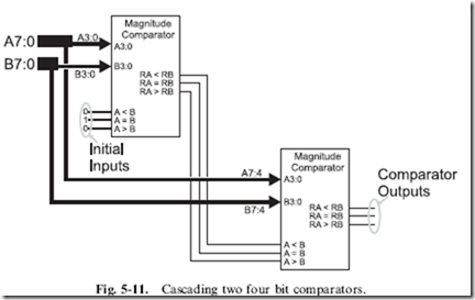
As well as indicating a complete set of related bits, a bus may be broken up into subsets, as shown in Fig. 5-11. In this diagram, I have shown how two four bit magnitude comparators can be ‘‘ganged’’ together to provide a comparison function on eight bits. The least significant four bits are passed to the first magnitude comparator and the most significant four bits are passed to the second magnitude comparator. The bits are typically listed as shown in Fig. 5-11, with the most significant bit listed first and separated from the least significant bit by a colon. In very few cases will you see the width of the bus reduced to indicate a subset of bits as I have done in Fig. 5-11;  most design systems will keep the same width for a bus, even if one bit is  being used in it.

image

Before going on, I want to make some comments about Fig. 5-11 as it provides a function that is often required when more bits must be operated on than is available by basic TTL or CMOS logic chips. To carry out the magnitude comparison operation on eight bits, I used two four bit magnitude comparator chips (modeled on the 7485) with the initial state inputs (marked ‘‘Initial Inputs’’ on Fig. 5-11) to start the chip off in the ‘‘neutral’’ state as if everything ‘‘upstream’’ (before) was equal to each other and the chip’s bits as well as any ‘‘downstream’’ (after) bits will determine which value is greater or if the two values are equal. This is a typical method for combining multiple chips to provide the capability to process more bits than one chip is able to.

Multiplication and Division

As you’ve read through this chapter, you should have noticed that there are usually many different ways of implementing different digital electronics functions. Each of the different implementation methods have their own advantages and tradeoffs – it is up to the application designer to understand what are the important ones. Nowhere is this more true than when you start discussing multiplication and division; there are a number of different methods of performing these arithmetic operations, each with their own characteristics.

Off the top of my head, I can come up with five different ways to multiply two binary numbers together. Before listing the different methods, I should make sure that I have defined the terms used in multiplication. The ‘‘multiplicand’’ is the value that is multiplied by the ‘‘multiplier’’ and typically remains static. The ‘‘multiplier’’ is the number of times that the multiplicand is added together to form the result or ‘‘product’’.

It should go without saying that if you had to multiply by a power of 2 (i.e.

1, 2, 4, 8, 16, etc.) a true multiplication operation is not required at all; the

operation can be accomplished by shifting the multiplicand. For example to

multiply a value by 4, you would simply shift the value to the left two times.

Division is the same, except the value is shifted to the right.

Understanding the basic terms ‘‘multiplier’’ and ‘‘multiplicand’’ leads to a

second method to implement a multiplication function in software – the

multiplicand is added multiplier number of times to the product. It can be

written out in ‘‘C’’ as: .

image

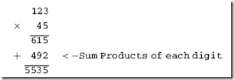
This method is painfully slow (especially for large multiplier values) and is difficult to implement in combinatorial digital logic. It is also different from the method which you were taught in school in which the multiplicand is shifted up by the radix for each digit of the multiplier. Using this method, ‘‘123’’ decimal is multiplied by ‘‘24’’ decimal in the format:

image

In the first line of the solution, I multiplied the multiplicand ‘‘123’’ by the least significant digit of the multiplier followed by multiplying the multiplicand by 10 (the radix) followed by the next significant digit of the multiplier. Once the multiplicand has been multiplied by each digit of the multiplier (along with the appropriate multiplication of the digit position), each product is added together to get the final result.

This method lends itself extremely well to working within binary systems. Rather than multiplying the multiplicand repeated by the radix for each digit,

the multiplicand is simply shifted to the right (which is multiplying by two) for each bit of the multiplier. If the multiplier bit is zero, then the value added to the product is zero. The binary multiplication operation for 123 by 45 is:

image

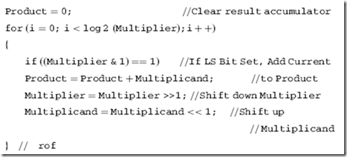
This is much more efficient than the previous version in terms of execution time and not significantly more complex than the other version. The ‘‘C’’ code that implements it is:

image

The first version is known as ‘‘Order n’’ because it loops once for each value of the multiplier. The shift and add version shown directly above is known as ‘‘Order log2’’ because it executes the log2 of the word size of the multiplier. For the eight bit multiplication example shown here, for the first method, up to 255 loops (and addition operations) may have to be executed. For the second example, a maximum of 8 loops (one for each bit, which is a simple way to calculate log2 of a number) is required.

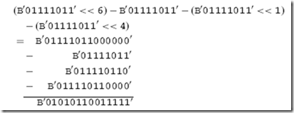
The final method of multiplying two numbers together is known as ‘‘Booth’s algorithm’’ and looks for opportunities to reduce the number of addition operations that are required by rounding the multiplier up and then adjusting the product by subtracting the multiplier’s zero bits that were ignored. For the example given in this section (123 multiplied by 45), Booth’s algorithm would recognize that 45, B’00101101’ rounds up to 64 (B’01000000’). Multiplying a binary number by 64 is the same as shifting left six times.

To adjust the product, the basic multiplicand (multiplied by 1) along with

all the instances where the multiplier has bit value of zero (in this case, bits one and four) have to be taken away from the rounded up value. For this example, the multiplication operation would look like:

image

which is the same result as we got above for a bit less work. Booth’s algorithm can produce a product in fewer, the same or more addition/subtraction operations as the previous method, so care must be taken to make sure that it is only used when it is going to provide an advantage.

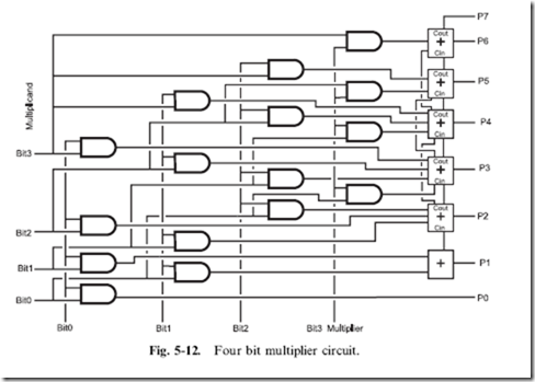
Each of the three methods presented so far requires the ability to ‘‘loop’’ through multiple iterations. This is a problem for most digital electronic circuits, as it not only requires a ‘‘clock’’ to synchronize the operations but it will also most likely take up more time than is desired. When a digital logic multiplier is designed, it typically looks something like Fig. 5-12. This circuit is wired to add all the multiplicand bits together for each possible multiplier values.

The multiplier bits are taken into account by ANDing them with each of the multiplicand bits. If a multiplier bit is zero, then the shifted up multiplicand bits are not passed to the multi-bit adders.

There are a couple points about the multi-bit adders that you should be

aware of. The first is that the maximum number of input bits for the adders used in the multiplier circuit is the number of bits in the multiplicand plus the log2 value of the multiplier. Secondly, as drawn, the adders are connected in a ‘‘ripple’’ configuration – a commercial circuit would probably wire the .

image

adders together as a carry look-ahead to minimize the time required for the multiplication operation to take place.

Before leaving the topic of multiplication, I should point out that all the methods presented here will handle multiplication of two’s complement negative numbers ‘‘natively’’. This is to say that no additional gates must be added to support the multiplicand or multiplier being negative.

Division is significantly more difficult to implement and is very rarely implemented in low-cost devices. Handling negative values considerably complicates the division operation and in this section, as well as most commercial solutions, negative values cannot be used for the dividend or divisor. To avoid the hardware complexities of division, software intensive solutions are normally done such as a repeated subtraction:

image

The bit shifting method shown for multiplication can also be used, but before comparisons can start, the divisor should be shifted up the word size of the dividend. To follow the bit shifting division code listed below you might want to do a thought experiment and single step through it with arbitrary values to see exactly how it works:

image

At the end of both these division algorithms, ‘‘Quotient’’ contains the quotient of the division operation and ‘‘Dividend’’ contains the remainder.

The bit shifting division algorithm could be implemented using digital

electronic gates as I demonstrated for the bit shifting multiplication algorithm, but you will find that it is quite a bit more complex than the bit shifting multiplication application in Fig. 5-12. This does not mean that there are some tricks you cannot implement if a division operation is required.

For example, if you wanted to divide a value by a known, constant value,

you could multiply it by its fraction of 256 (rather than the typical 1) and then divide by 256 (which is accomplished by shifting right by eight bits). For example, dividing 123 by 5 would be accomplished by multiplying 123 by 51 (256 divided by 5) and shifting the product (6,273) to the right by 8 bits to get the result 24. While this method seems like it’s complex, it is actually quite easy to implement in digital electronics.

Quiz

1. 6 – 5 is the same as:

(a) 6+ (-5)

(b) 5 – 6

(c) 999999

(d) B’1111 1111’

2. In a universe where infinity (the highest possible number) is one million (1,000,000); ‘‘-11’’ could be represented as:

(a) Only -11

(b)

999,988

(c)

999,989

(d)

89

3. A ‘‘half adder’’:

(a) Can perform an addition operation on two bits

(b) Can add half the bits together of an addition operation

(c) Combines the ‘‘carry’’ outputs of a ‘‘full adder’’ to produce the correct result

(d) Is built from half the number of gates as a full adder

4. A ‘‘ripple adder’’ is not used in a PC or workstation processor because:

(a) Its complexity can affect the operation of other arithmetic functions

(b) The result is often wrong by one or two bits

(c) The delay required for the signal to pass through the gates can be unacceptably long

(d) It cannot handle the 32 or 64 bit addition operations required

5. B’10’ – B’01’ passed through two full subtracters produces the result:

(a) Cannot be done because a borrow operation is required

(b) B’01’ with borrow ¼ 1

(c) B’10’ with borrow ¼ 0

(d) B’01’ with borrow ¼ 0

6. Converting the four bit, two’s complement value ‘‘-4’’ to a positive number by inverting each bit and incrementing the result produces the bit pattern:

(a) B’0100’

(b) Which is five bits long and is invalid (c) B’0011’

(d) B’1100’

7. Busses are made up of:

(a) Multiple bits of a single value

(b) Multiple bits passing to the same subsystem of the application

(c) The highest speed signals in the application

(d) Related bits

8. Multiplying two four bit numbers by repeated addition:

(a) Will require up to 4 addition operations

(b) Will require up to 15 addition operations

(c) Cannot be implemented in digital electronics

(d) Is the fastest way of performing binary multiplication

9. Multiplying a binary number by 16 can be accomplished by:

(a) Clearing the least significant four bits

(b) Shifting left four bits

(c) Shifting right four bits

(d) Setting the least significant four bits

10. Dividing an eight bit value by the constant value 6 is best accomplished by:

(a) Using the repeated subtraction method

(b) Using the bit shifting method

(c) Shifting the value to the right by two and then shifting the value to the right by 1 and adding the two values.

(d) Multiplying by 256/6 (42) and shifting the product to the right

by 8 bits


Binary Arithmetic Using Digital Electronics : Adders

Binary Arithmetic Using Digital Electronics

Before going into showing how basic binary arithmetic operations are performed in digital electronic circuits, I thought it would be useful to review how you would perform basic arithmetic operations. Before discussing how many binary arithmetic operations there are, some different characteristics of binary numbers should be discussed. I realize that much of the material in this chapter introduction is a review of work that you first did in grade school, but often when confronted with situations that require you to develop binary arithmetic operations in digital electronics, this basic information can easily be forgotten and standard devices that provide this function are often overlooked.

image

When you first learned to add decimal numbers together, you probably were required to memorize all 100 different combinations of single digit parameters when only 55 are really required. In Table 5-1, I have listed the 55 pairs which have to be memorized; the remaining 45 pairs do not have to be memorized because of the commutative law which states:

A + B =B + A

and means that the number pairs like ‘‘4+7’’ and ‘‘7+ 4’’ are equivalent.

The result of adding each of these two parameters produces either a single digit or double digit sum. The double digit sum indicates that the value of the result is greater than could be represented in a single digit of the number base. For decimal numbers, the maximum value that can be represented by a single digit is ‘‘9’’. Looking at the general case, the maximum value that can be represented by a number system is the base minus one. So, for the binary number system (base 2), the maximum value is ‘‘1’’; for hexadecimal (base 16), the maximum value is ‘‘15’’ (or ‘‘0x0F’’).

The leftmost digit of a double digit number is known as the ‘‘carry’’ digit.

In Chapter 4, I showed how multi-digit numbers are made up of single digit values multiplied by powers of their base. Knowing the sums of the 55 addition pairs of Table 5-1, multi-digit numbers can be added together

image

by working through pairs of numbers, as I show in Fig. 5-1. This is a rather pedantic way of showing addition and I’m sure that when you add two multi- digit numbers together, you are much more efficient, but when you were learning, this was probably the process that you went through.

While saying that you are much more efficient, it really comes down to the idea that you are able to recognize that one plus another number is the same as incrementing the other number. You are still only adding one digit at a time and the carry is ‘‘rippling’’ to the next significant digit. Carry ‘‘ripple’’ is an important concept that will be discussed in more detail in the next section.

Subtraction has many of the same issues as addition, but with some additional complexities. The first being that you cannot simplify your memorization of the 100 pairs of subtracted parameters as you did for addition; the commutative law does not apply to subtraction as it did for addition. For example,

imageNext, if the number being taken away is greater than the original number, the result (or ‘‘difference’’) could be less than 0 or ‘‘negative’’. There is a very big question on how to represent that negative number. Typically, it is represented as a value with a ‘‘minus’’ or ‘‘subtraction’’ sign in front of it, e.g. ‘‘-2’’.

The minus sign is only used when the digit cannot ‘‘borrow’’ from the next significant digit, as shown in Fig. 5-2. The result of 25 minus 9 is 16, with the ones borrowing 10 from the tens column (the next significant digit) to allow the operation to proceed without a negative result.

image

Subtraction can also be expressed as adding a negative value and can be written out as:

imageThis should not be a surprise to you unless you consider the following philosophical question: What would happen if infinity was arbitrarily defined as one million (1,000,000)? Instead of adding a minus sign to our value to make it negative, we could subtract it from ‘‘infinity’’.

For example, if we had the problem:

imagewe could define ‘‘-5’’ as one million subtract 5 or ‘‘999,995’’. Now, going back to the addition of the negative number and substituting in ‘‘999,995’’ for ‘‘-5’’ we get:

image

Since a million is defined as infinity and has no meaning, it can be taken away from the result, leaving us with the difference of 8 minus 5 being ‘‘3’’. This method may seem to be overly complex, but I will show you how this applies to digital electronics later in the chapter.

Like addition, the method presented here for subtraction is carried out a single digit at a time with the need to borrow from the next more significant digit being similar to passing the carry digit in addition. Like the ‘‘ripple carry’’ in addition, the ‘‘borrow’’ in subtraction can also be thought of as a ‘‘ripple’’ operation.

Multiplication and division have, not surprisingly, many of the same issues and when I discuss them later in this chapter, I will review them with you. Before reading the section discussing multiplication and division, I suggest that you review these operations and try to think of how they can be accomplished using digital electronics.

Adders

The circuit shown in Fig. 5-3 will add two bits together and output the sum (‘‘S’’) bit along with a carry (‘‘C’’) bit, if both inputs are ‘‘1’’ and the sum is ‘‘2’’, which is greater than the maximum number that can be represented by the number base (which is 1 for binary). Table 5-2 is a truth table, showing the output of each bit for different input values. You should be able to see that the ‘‘sum’’ bit is 1 when one or the other (but not both) of the two input bits is 1 and the ‘‘carry’’ bit is 1 only when both input bits are 1.

image

image

The adder is the first practical use most people have for the XOR gate and its function can be seen very clearly in Table 5-2 for the sum bit. Along with the XOR gate providing the function for the sum bit, you should also recognize that the carry bit is the output of a simple AND gate.

This simple digital electronic circuit is known as a ‘‘half adder’’ because it will handle half the operations required of the general case addition circuit. The ‘‘full adder’’ (Fig. 5-4) starts with a half adder and adds another bit (which is the less significant bit’s ‘‘carry’’ output) to its sum. Put another way, the full adder adds three individual bits together (two bits being the digit inputs and the third bit assumed to be carry from the addition of the next least-significant bit addition operation, known as ‘‘Cin’’).

You can analyze the operation of the full adder to check on its operation.

The sum bit is 1 only if one or three of the input bits is 1. In the half adder, I showed that the sum bit could be written out as:

imageand should only be ‘‘1’’ if only one of the two inputs was 1. To understand the logic required to produce the sum bit for the three bit full adder, I created Table 5-3 in which the XOR output of the A and B inputs was given a single column entry. From the data presented in this table, you can see that the sum could be expressed as:

image

image

which, if you look back at Fig. 5-4, is exactly how it is implemented in the ‘‘full adder’’.

The carry output bit is 1 if two or three of the input bits are 1. As an

exercise, you may wish to create a truth table and reduce it down to see if you can match the carry gate logic of Fig. 5-3, but you can write out and reduce a sum of products equation quite easily:

image

image

which is exactly the carry logic circuit shown in Fig. 5-2. This type of analysis is useful to do when you are trying to puzzle out what a circuit is doing or to confirm that it is doing exactly what you expect it to do. It is also good practice of using the logic equation optimization skills first presented in Chapter 2.

Multiple full adders can be chained together (like in Fig. 5-5) to produce a multi-bit adder in which the carry results for each bit ‘‘ripples’’ through the various adder circuits. For most applications, this ‘‘ripple carry adder’’ can be used safely, but in something like your PC’s processor, where quite a few bits are required and the adder is expected to execute quickly, the time required for the carry to ripple through the adders is prohibitive.

The solution to this problem is the ‘‘carry look-ahead’’ adder in which each bit takes not only the appropriate bits for input but also all the least

significant bits that can affect the bit. The length of time the carry look-ahead adder needs to produce a sum is generally independent of the number of bits in the operation (unlike the time the ripple adder requires to produce a sum which is a function of the number of bits). Table 5-4 lists the different inputs and expected outputs for a three bit carry look-ahead adder. Reducing the

Table 5-4 Carry look-ahead adder input/output truth table.

A2

B2

A1

B1

A0

B0

S0

S1

S2

Carry

0

0

0

0

0

0

0

0

0

0

0

0

0

0

0

1

1

0

0

0

0

0

0

0

1

1

0

1

0

0

0

0

0

0

1

0

1

0

0

0

0

0

0

1

1

0

1

1

0

0

0

0

0

1

1

1

0

0

1

0

0

0

0

1

0

1

1

1

0

0

0

0

0

1

0

0

0

1

0

0

0

0

1

1

0

0

0

0

1

0

0

0

1

1

0

1

1

0

1

0

0

0

1

1

1

1

0

1

1

0

0

0

1

1

1

0

1

0

1

0

0

0

1

0

1

0

1

1

0

0

0

0

1

0

1

1

0

0

1

0

0

0

1

0

0

1

1

1

0

0

0

0

1

0

0

0

0

1

0

0

0

1

1

0

0

0

0

1

1

0

0

1

1

0

0

1

1

1

1

0

0

1

1

0

1

1

0

0

0

1

0

1

1

0

1

0

1

1

1

0

0

1

1

1

1

0

1

0

0

1

Table 5-4 Continued.

A2

B2

A1

B1

A0

B0

S0

S1

S2

Carry

0

1

1

1

1

1

0

1

0

1

0

1

1

1

0

1

1

0

0

1

0

1

1

1

0

0

0

0

0

1

0

1

0

1

0

0

0

1

1

0

0

1

0

1

0

1

1

1

1

0

0

1

0

1

1

1

0

0

0

1

0

1

0

1

1

0

1

1

1

0

0

1

0

0

1

0

1

0

1

0

0

1

0

0

1

1

0

1

1

0

0

1

0

0

0

1

1

0

1

0

0

1

0

0

0

0

0

0

1

0

1

1

0

0

0

0

0

0

0

1

1

1

0

0

0

1

1

0

0

1

1

1

0

0

1

1

0

1

0

1

1

1

0

0

1

0

1

0

0

1

1

1

0

1

1

0

1

1

0

1

1

1

0

1

1

1

0

0

1

1

1

1

0

1

0

1

1

1

0

1

1

1

0

1

0

0

0

1

0

1

1

1

1

1

0

0

0

0

1

1

1

1

1

1

0

1

1

0

1

1

Table 5-4 Continued.

A2

B2

A1

B1

A0

B0

S0

S1

S2

Carry

1

1

1

1

1

1

0

1

1

1

1

1

1

1

1

0

1

0

1

1

1

1

1

0

1

0

1

1

0

1

1

1

1

0

1

1

0

0

1

1

1

1

1

0

0

1

1

1

0

1

1

1

1

0

0

0

0

1

0

1

1

0

1

0

0

0

0

1

1

0

1

0

1

0

0

1

1

1

1

0

1

0

1

0

1

1

0

0

0

1

1

0

1

0

1

0

1

1

1

0

1

0

1

1

1

0

1

0

0

1

1

0

1

1

1

1

0

1

0

1

1

0

1

1

0

1

1

0

0

1

1

0

1

1

0

0

0

0

0

1

1

0

0

1

0

0

0

1

1

0

1

0

0

1

0

1

1

1

1

0

1

0

0

1

1

1

0

0

0

1

1

0

0

1

1

0

1

1

1

0

1

0

0

0

1

0

1

0

1

0

1

0

0

0

1

1

0

1

1

0

1

0

0

0

0

1

1

0

1

0

1

0

0

0

0

0

0

0

1

0

information from this table, I have listed the equations for the three sum bits and the carry bit below:

image

It was a major effort on my part to reduce the equations for each sum bit and the carry bit. To do this, I used the truth table reduction method discussed in Chapter 2. To reduce the number of terms in the resulting sum of products equations, I first deleted all the instances where the specific bit was not ‘‘1’’ – in every case, this reduced the number of instances by half. Next, I worked at combining instances that were similar and found that rather than combining ‘‘don’t care’’ bits, I found a number of places where two bits were XORed together. In the resulting equations, I kept the ‘‘XOR’’ terms in, even though when the ‘‘technology optimization’’ stage of the development effort is completed, these gates will be reduced to the technology’s basic gates.

If you read through the equations and try to understand them, you will find that they do make a kind of sense. Obviously, as more bits are added to the carry look-ahead adder, the circuit becomes much more complex. Despite this complexity, the carry look-ahead is the most efficient way to provide an adder circuit for large bit words in fast applications.


Number Systems :Binary Coded Decimal and Gray Codes

Binary Coded Decimal

In the early days of programming, data structures were often the result of a curious blend of trying to come up with a data format that best suited the programmer and what best suited the current hardware. One of the more

Table 4-5 Decimal digits with binary and BCD decimal equivalents.

Decimal

Binary

BCD

Decimal

Binary

BCD

0

B’0000’

0

8

B’1000’

8

1

B’0001’

1

9

B’1001’

9

2

B’0010’

2

10

B’1010’

Invalid

3

B’0011’

3

11

B’1011’

Invalid

4

B’0100’

4

12

B’1100’

Invalid

5

B’0101’

5

13

B’1101’

Invalid

6

B’0110’

6

14

B’1110’

Invalid

7

B’0111’

7

15

B’1111’

Invalid

enduring structures that came from this time is the ‘‘binary coded decimal’’ (most often referred to by its acronym ‘‘BCD’’) which used four bits, like hexadecimal values, but only allowed the values of zero through nine rather than the full 16 values that were possible (as shown in Table 4-5). The reason for using this data structure has largely disappeared in computer systems, but it is still a viable and useful method of handling data in digital electronics and one that you should keep in your ‘‘hip pocket’’ when you design circuits.

The original reason for using the BCD data format in computer programming was its elimination of the need to add code to the program to convert a binary or hex number into decimal. The code storage required for the conversion was expensive and the processors were nowhere near as possible as what is available today. Using decimal values was actually an optimal way of processing data in these old systems.

The lasting legacy of this is the number of standard chips that can process BCD values just as easily as other standard chips can process hexadecimal values and will allow you to design circuitry that works with decimal values just as easily as if you were working with hex values.

While this is getting a bit ahead of things, I want to give the example of designing a delay that holds back a signal for 100 seconds. Using traditional binary logic, which only works with bits that are a power of two, you would have to design a circuit that compares a counter value and indicates when the

value ‘‘100’’ was reached and reset itself. When using digital electronic chips that are designed for BCD values, the comparator function is not required, as each BCD digit cannot be greater than ‘‘9’’ and, cascaded together, they can only count to a maximum value of ‘‘99’’ to ‘‘00’’.

This may seem like a trivial example, but you will find a number of cases like this one where you will have to create circuits that work on base 10 data and by using chips which are designed for BCD values, the complexity of your work will be greatly reduced.

Going back to Table 4-5, the production of the ‘‘invalid’’ indication is

worthy of some discussion as it provides a good example of how gate optimization is not always as straightforward as you might expect.

In most BCD chips, if the value of 10 or more is passed in the binary bits, then the value is converted to zero and a carry indication is output. Using the tools presented in Chapter 2, you should be able to derive the sum of products formula for the positive active ‘‘invalid’’ indicator as:

imageand using the conversion formulas of Chapter 2, you would simplify the ‘‘invalid’’ formula above to:

image

Figure 4-1 shows the AND/OR gates for this function along with the ‘‘NAND equivalent’’ function beneath it. The NAND equivalent was chosen by assuming that the function would be implemented in TTL. While this circuit looks a bit complex, if you follow it through, you will find that it provides the same function as the AND/OR combination above it.

It will probably surprise you to find out that this circuit is not optimal by any measurement: you can do better in terms of the number of gates, the time

image

it takes a signal to pass through the gates and in providing a constantly timed output. The circuit at the bottom half of Fig. 4-1 will respond in two gate delays if A3 changes and in four gate delays if A2 changes. For many circuits, this is not a problem, but when you are working with high-performance designs, a variable output delay can result in the application not working correctly and being almost impossible to debug.

A much better approach to optimizing the circuit is to work at converting it to the basic gate used by the technology that you are working with and then optimizing this. Going back to the original ‘‘Invalid’’ equation:

imageI can convert the OR to a NAND, by inverting its two parameters (according to De Morgan’s theorem), ending up with:

imageIt is probably astounding to see that the function provided by the mess of NAND gates in Fig. 4-1 can be reduced to the three simple gates required by the formula above. Along with reducing the number of gates, you should also notice that the maximum number of gate delays is two, regardless of which bit changes.

Looking at the NAND circuits in both diagrams, you are probably  at a loss as to how you could reduce the NAND circuit in Fig. 4-1 to the three

image

gates of the optimized circuit. Personally, I would be surprised if you could; when I look at the two circuits, they look like they provide completely different functions.

What I want to leave you with is an example of how looking at a logic function from different perspectives can result in radically different circuits

with surprisingly different parameters. In the first case, I reduced three gates to two, to end up with six NAND gates, while in the second, I avoided reducing the basic function and converted it directly to a much more efficient three NAND gate circuit.

In going through this exercise to produce the ‘‘invalid’’ output for BCD, I hope that you can apply this knowledge for creating circuits that work with different base systems than just a power of two. In some cases, you may have to work with numbers that are base 9 or 13 and using the example here, you should have some idea of how to keep the values within certain ‘‘bounds’’.

Gray Codes

I hope I have convinced you of the usefulness of using Gray codes for inputs when you are illustrating how digital electronic logic functions respond to inputs. I must point out, however, that Gray codes were originally created for a much different function – they were designed for use in position sensors as the single changing bit allowed hardware to be designed to respond to a single changing bit and not the potentially several bits of a binary sequence. By only changing one bit at a time, absolutely precise positioning of marking sensors (causing all changing bits being sensed at the exact same instant) was not required.

Gray codes were invented by Frank Gray of Bell Labs in the mid 1950s and has a ‘‘hamming value’’ of 1. The hamming value is the number of bits that change between one value and the next. A four bit binary number can have all four bits change as it increments or decrements; a Gray code never has more than one bit change during incrementing or decrementing operations.

Chances are, you would not have any trouble coming up with a two bit Gray code (b’00’, b’01’, b’11’ and b’10’) and in a pinch, you would be able to come up with a three bit Gray code (b’000’, b’001’, b’011’, b’010’, b’110’, b’111’, b’101’ and b’100’). I suspect that if you were given the task of coming up with any more bits than this, you would be stumped.

In trying to come up with a way of explaining how Gray codes worked, I noticed that when a new most significant bit was set, the previous values were ORed with this bit, but written out in reverse order. In some texts, this property is recognized by calling Gray codes a binary reflected code. Looking at Table 4-6, you can see that I created a four bit

image

Gray code by taking the eight values of the three bit code, reversing them and setting bit 3.

This could be written out as a computer program algorithm as:

image

This code demonstrates how Gray codes are produced, but is not the optimal method for producing Gray codes (it is actually an ‘‘order n2’’ algorithm, which means that every time the number of bits is doubled, the amount of time required to produce the values is quadrupled). Along with this, it is not easy to create digital logic hardware that will create these codes.

Fortunately, individual binary codes can be converted to Gray codes using the circuit shown in Fig. 4-2, which simply implements the formula:

imageGoing the other way (from Gray code to binary) is a bit more complex and while it uses n – 1 (where ‘‘n’’ is the number of bits) XOR gates, like converting binary codes to Gray codes, the output of each XOR gate is required as an input to the next least significant bit, as shown in Fig. 4-3. The output of the circuit is not correct until the most significant bit has passed through each of the XOR gates to the least significant bit.To perform the data conversion a simple formula cannot be used. Instead  the following algorithm is required:

image

image

I find it very difficult to explain exactly how this code works, except to say that with each iteration of the while loop, the ‘‘Gray code’’ value gets shifted down more and more to move the most significant bits into position for XORing with the less significant bits. To convince yourself that the algorithm works, you might want to perform a ‘‘thought experiment’’ on it and list the changing value of ‘‘Gray code’’ as I have done in Table 4-7.

In this chapter, more than anywhere else in the book, I have used sample computer programs to show how different values can be produced. This is a somewhat different approach to explaining how multi-bit binary data conversions are implemented and one that takes advantage of the ubiquity of the personal computer and the ability of most technical students to perform even rudimentary programming.

Using computer code to help demonstrate how the conversions are done should also give you another method for processing binary values as well as of testing formulas and optimizations. I always find it useful to have a number of different ways to solve a problem, or test a potential solution,

Table 4-7 Working through the shifting values of the Gray code convention algorithm.

Initial bit values

Shift ¼ 1 bit values

Shift ¼ 2 bit values

Shift ¼ 4 bit values

B7

B7

B7

B7

B6

B6 ^ B7

B6 ^ B7

B6 ^ B7

B5

B5 ^ B6

B5 ^ B6 ^ B7

B5 ^ B6 ^ B7

B4

B4 ^ B5

B4 ^ B5 ^ B6 ^ B7

B4 ^ B5 ^ B6 ^ B7

B3

B3 ^ B4

B3 ^ B4 ^ B5 ^ B6

B3 ^ B4 ^ B5 ^ B6 ^ B7

B2

B2 ^ B3

B2 ^ B3 ^ B4 ^ B5

B2 ^ B3 ^ B4 ^ B5

^ B6 ^ B7

B1

B1 ^ B2

B1 ^ B2 ^ B3 ^ B4

B1 ^ B2 ^ B3 ^ B4 ^ B5 ^ B6 ^ B7

B0

B0 ^ B1

B0 ^ B1 ^ B2 ^ B3

B0 ^ B1 ^ B2 ^ B3 ^ B4 ^ B5 ^ B6 ^ B7

and I suggest that along with the various tools and computer algorithms presented in this book that you try to come up with methods for yourself that will help you design and test digital electronic circuits more efficiently.

Quiz

1. If you had a number system that was base 5, the most significant value in a digit would be:

(a)

6

(b)

10

(c)

4

(d)

5

2. The eight bit binary equivalent to decimal 47 is: (a) 0010 1111

(b) B’0010 1111’

(c) 101111

(d) 1011 11

3. The third most significant digit in the decimal number ‘‘1234’’ is:

(a) The hundreds column

(b) 3

(c) 1

(d) No digit can be the third most significant

4. To verbally tell somebody the hex number value 0x04AC you would say:

(a) ‘‘Four-Able-Charlie’’

(b) ‘‘Hexadecimal Four-Eh-See’’

(c) ‘‘Hexadecimal Four-Apple-Charlie’’

(d) ‘‘Hexadecimal Four-Able-Charlie’’

5. The decimal number ‘‘123’’ in hexadecimal is:

(a) 0x0123

(b) B’0111 1011’

(c) 7B

(d) 0x07B

6. The four bit hexadecimal number 0x01234 expressed in decimal is:

(a) 1,234

(b) 4,660

(c) B’0001 0010 0011 0100’

(d) 0x04D2

7. Binary coded decimal is defined as:

(a) Ten bits providing ten different values

(b) Four bits providing ten numeric values and six control codes

(c) Four bits providing ten numeric values

(d) Five bits with each bit providing two values for a total of 10

8. BCD should:

(a) Never be used

(b) Used with circuits that operate with base 10 numbers

(c) Only be used when you’ve run out of binary chips

(d) Used when values are not expected to exceed 9

9. B’0110’ in binary, using the formula Gray code ¼ binary ^ (binary » 1) can be converted to the Gray code:

(a) B’1010’

(b) B’0110’

(c) B’0101’

(d) B’0111’

10. The Gray code B’0010’ corresponds to the binary value: (a) B’0011’

(b) Unknown because more data is required (c) B’1101’

(d) B’0010’


Number Systems : Base 16 or Hexadecimal Numbers

Number Systems

Working through the book to this point, you should be comfortable with combining multiple single bit values together in a variety of different ways to perform different combinatorial circuit functions. Along with being able to meet the basic requirements, you should be able to optimize the circuit to the fewest number of gates that is available within the technology that you are going to use. This skill is very useful in itself, but it is only scratching the surface of what can be done with digital electronics; most data consists of more than a single bit (which can have only two values) to process, and working with multiple single bits of data can be cumbersome. What is needed is a methodology for combining bits together so they can represent larger values that can be simply expressed.

The solution to this issue is to combine bits in exactly the same way as a 10-value character is combined to produce the decimal numbers that you are familiar with. While on the surface, combining bits does not seem to be directly analogous to decimal numbers, by using the same method that decimal numbers are produced, multi-bit numbers (which are most often described as ‘‘binary’’) numbers can be produced.

In primary school, you learned that the four-digit number ‘‘1,234’’ was built out of four digits, any of which could have the 10 values ‘‘0’’, ‘‘1’’, ‘‘2’’,‘‘3’’, ‘‘4’’, ‘‘5’’, ‘‘6’’, ‘‘7’’, ‘‘8’’ and ‘‘9’’. When listing the different values for a digit, zero is stated because the number ‘‘10’’ is actually a two digit number. The number of different values for each digit is referred to as its ‘‘base’’ or ‘‘radix’’. It is important to note that the first value is always zero and the last value is the base minus one.

When expressing each digit, its value was stated by the ‘‘column’’ it was in (‘‘ones’’, ‘‘tens’’, ‘‘hundreds’’, ‘‘thousands’’, etc.). For example, the second column of ‘‘1,234’’ is the ‘‘hundreds’’ column and in 1234, there are two hundreds.

In high school, you would have been introduced to the concept of exponents and instead of expressing each digit in the number by the column, you would express it by the digit multiplier. So, 1,234 could now be written out as:

image

The beauty of expressing a number in this way is that each digit’s multiplier is mathematically defined as a power of the base. Using this format, it is possible to create a numbering system using single bits to represent ‘‘binary’’ numbers.

For example, four bits could be put together with the bit containing the least significant digit labelled ‘‘Bit0’’, the second least significant as ‘‘Bit1’’, the second most significant as ‘‘Bit2’’ and the most significant as ‘‘Bit3’’. The term significance when applied to bits is used to express the magnitude of the bit’s multiplier. For example, Bit0, which is multiplied by 20 or 1, has less significance than Bit3 which is multiplied by 23 or 8.

Using the same exponent format as was used to define the decimal number 1,234, the four-bit binary number could be defined as:

image

and written out in a similar format to a decimal number. Collectively, the number is written out as a series of ones and zeros, in a similar manner to that of a decimal number.

Many books go into great length trying to explain how to convert a decimal number to a binary number. I won’t go into the same amount of detail because the algorithm to do this is really quite simple: you simply start at some most power of two and work your way down, writing out a ‘‘1’’ for each time the subtraction the power of two results in a positive number or zero and a ‘‘0’’ when the difference is negative.

Written out as part of a ‘‘C’’ program, converting a decimal number to a character four-bit binary number is accomplished by the following statements:

image

Note that I start at ‘‘4’’ and subtract one for the actual bit value in the example code above.

Demonstrating the algorithm, consider the case where you wanted to express the decimal number ‘‘11’’ as a four-bit decimal. In Table 4-1, I have listed each step of the program with the variable values at each step.

Converting binary numbers to decimal is very easy because the power of two of each digit that has a value of ‘‘1’’ are summed together. The ‘‘C’’ code

image

image

to convert a value in ‘‘Bit’’ to a decimal value is:

image

In Table 4-2, I have listed the process of converting the binary number 0110 to decimal and you should note that I have highlighted the bit that is being tested.

Before going on, I would like to point out that there can be a lot of confusion with regards to using binary numbers with decimal numbers or numbers of different bases. To eliminate the confusion, you should always identify the binary numbers by placing a percentage sign (‘‘%’’) or surrounding it with the letter ‘‘B’’ and two single quotes (‘‘ ’ ’’). Using these conventions, the bit pattern converted in Table 4-1 would be written out as %0110 or B’0110’. The % character put before a binary number is a common assembly language programming convention. The letter ‘‘B’’ and the single quotes around the number is the format used in ‘‘C’’ programming and will be the convention that I use in this book.

Another area of confusion with regards to binary numbers is how they are broken up for easier reading. Each group of three digits in a decimal number is usually separated from other groups of digits by use of a comma (‘‘,’’ in North America and a period or dot (‘‘.’’) in Europe and other parts of the world). When working with binary numbers, instead of separating each three digit group with a punctuation character, it is customary to use a blank to separate four digit groups. Using the conventions outlined here, the eight bit number 10111101 would be written out as:

imageThis is the binary number format convention that I will use for the rest of the book.

Base 16 or Hexadecimal Numbers

As I will show in this and the next section, having programming experience is a two-edged sword – it will help you understand certain concepts (such as the ‘‘bit’’ and some data structures like the ones presented in this and the next section), but it will blind you to other opportunities. The goal of these sections is to illustrate how bits can be grouped together to make your design efforts more efficient as well as making it easier for you to both see possibilities for the design and articulate them to other people.

Creating binary numbers from groups of bits, as I demonstrated in the introduction to this chapter, is quite easy to do, but can be very cumbersome to write out as well as transfer correctly. You may also have difficulty in figuring out exactly how to express the number, asking should it be passed along starting from the most significant or least significant bit. At the end of this chapter’s introduction, I left you with the number B’1011 1101’ and you should agree that telling somebody its value is quite cumbersome; for example, you might say something like, ‘‘The eight bit, binary number, starting with the most significant bit is one, zero, one, one, one, one, zero and one.’’

It is much more efficient to combine multiple bits together into a single entity or digit.

The most popular way of doing this is to combine four bits together as a ‘‘hexadecimal’’ digit which has 16 different values. This numbering system has a base of 16. If you are familiar with programming, chances are you are familiar with hexadecimal digits (which is often contracted to the term ‘‘hex’’), which I have listed out with their decimal and binary equivalents in Table 4-3.

To create a way of expressing the 16 values, the first 10 hexadecimal values are the same as the 10 decimal number values, with the following six being given letter codes. This is why I included the ‘‘phonetic’’ values for the hexadecimal values greater than 9; the letter names ‘‘B’’, ‘‘C’’ and ‘‘D’’ can be easily confused, but their phonetic representations are much clearer.

Table 4-3 Hexadecimal digits with binary, decimal equivalents and phonetic values.

Decimal

Binary

Hex

Phonetic

Decimal

Binary

Hex

Phonetic

0

B’0000’

0

Zero

8

B’1000’

8

Eight

1

B’0001’

1

One

9

B’1001’

9

Nine

2

B’0010’

2

Two

10

B’1010’

A

Able

3

B’0011’

3

Three

11

B’1011’

B

Baker

4

B’0100’

4

Four

12

B’1100’

C

Charlie

5

B’0101’

5

Five

13

B’1101’

D

Dog

6

B’0110’

6

Six

14

B’1110’

E

Easy

7

B’0111’

7

Seven

15

B’1111’

F

Fox

I tend to place a lot of importance to using conventions when expressing letters. You may be tempted to make up your own letter codes or use the aviation phonetic alphabet (Table 4-4) when communicating hexadecimal values to other people (‘‘AF’’ could be ‘‘Apple-Frank’’ or ‘‘Alpha-Foxtrot’’ instead of ‘‘Able-Fox’’). I would like to discourage this for two reasons: the first is that the person you are talking to will have to mentally convert your words into letters and then hex digits – this process is complicated when unexpected words are used. Secondly, I prefer using the phonetic codes in Table 4-3 for hex values and the aviation phonetic codes for letter codes.

Multi-digit hexadecimal numbers are written out in a similar way as decimal or binary numbers with each digit multiplied by 16 to the power of the number of value’s position. For a 16 bit number (four hexadecimal digits), the digit multipliers are listed below:

image

To indicate a hex number, you should use one of the programming conventions, such as putting the prefix ‘‘0x0’’ or ‘‘$’’ at the start of the hexadecimal

Table 4-4 Aviation phonetic codes.

Letter

Phonetic

Letter

Phonetic

Letter

Phonetic

A

Alpha

J

Juliet

S

Sierra

B

Beta

K

Kilo

T

Tango

C

Charlie

L

Lima

U

Uniform

D

Delta

M

Mike

V

Victor

E

Echo

N

November

W

Whiskey

F

Foxtrot

O

Oscar

X

X-Ray

G

Gulf

P

Papa

Y

Yankee

H

Hotel

Q

Quebec

Z

Zulu

I

India

R

Romeo

value. The same formatting convention used with binary numbers (X’##’, where ‘‘##’’ are the hex digits) could also be used. For this book, I will be expressing hexadecimal numbers in the format 0x0## which is visually very different from binary numbers, which should help to immediately differentiate them.

To convert a decimal number to a character 16 bit hexadecimal number, you can use the ‘‘C’’ algorithm shown below. Note that I have used the C modulo (‘‘%’’) operation which returns the remainder from an integer division operation and not its dividend.

image

Going the other way, to convert a four hexadecimal digit number to decimal you can use the algorithm:

image

Many books provide a conversion table between binary, hexadecimal and decimal numbers, but I would like you to be familiar with the conversion algorithms written out above as well as buy yourself an inexpensive scientific calculator which has ability to convert between base systems. The ability to convert between the base systems is actually quite simple and available in many basic scientific calculators which cost $10 or less. Understanding how to convert between base systems and having an inexpensive calculator will enable you to perform the conversions faster and with more flexibility than using a table, which is limited in the number of different values it can present.

If you are familiar with numbers in different languages, then you will know that the prefix ‘‘hex’’ actually refers to the number ‘‘six’’ and not ‘‘16’’. The actual prefix for 16 is the term ‘‘sex’’ and in the early days of computers, this was (obviously) a source of some amusement. When IBM introduced the System/360, in the early 1960s, the company was uncomfortable with releasing something that was programmed in ‘‘sexadecimal’’, fearing that it might upset some users. To avoid any controversy, all documentation for the System/360 was written using the 16 bit ‘‘hexadecimal’’ numbering system presented here. The System/360 was a wild success, becoming the first ‘‘computer for the masses’’ and many people’s first experience in program- ming and electronics. The term ‘‘hexadecimal’’ became the popular term for 16 bit numbers and displaced the more correct ‘‘sexadecimal.’’


Creating Digital Electronic:Logic Gate Input and Output ,Simple Digital Logic Circuit Development and Testing a Simple TTL Inverter

Logic Gate Input and Output

If you have worked with digital electronics before, you probably have made a few assumptions about how the circuitry works and how you can demonstrate how digital electronic devices work. Chances are many of these assumptions are with regard to how gate and chip inputs and outputs work as well as how to properly interface them together and to different electronic devices. These assumptions are generally made on the evidence of by what somebody has seen with a voltmeter or logic probe and do not look at the underlying circuitry and how it works. In this section, I will give you a detailed introduction to the input and output pins on digital electronics and how they should be wired.

When we talk about digital electronics, we should identify the different technologies used. ‘‘Transistor to transistor logic’’ (TTL) is based on NPN bipolar transistors. TTL chips have the part number prefix ‘‘74’’ (i.e. a chip with four, two input NAND gates known as the ‘‘7400’’). There are actually quite a few different technology chip families based on the 74xx ‘‘standard’’

pinout and operation and the technology is indicated by letter codes following the ‘‘74’’; a chip marked with ‘‘74LS00’’ is a low-power, Shotkey four two-input NAND gate chips. Many of these technologies used with the 7400 series of chips are based on bipolar transistors, but some are based on MOSFET technology. These MOSFET technology based chips have the 74 prefix and a technology letter code containing a ‘‘C’’ (i.e. ‘‘C’’, ‘‘HC’’, ‘‘HCT’’). Along with being used in 7400 series form factors, MOSFET devices are used in the ‘‘4000’’ series of logic chips. Understanding which type of transistor is used in a logic chip is critical to being able to successfully interface it to other chips or input/output devices.

When the term ‘‘TTL’’ is used, it is referring to bipolar transistor logic in

the 7400 series. ‘‘CMOS’’ indicates MOSFET transistor logic used in the 74C00 and 4000 chip logic series.

Probably the biggest erroneous assumption that people have about digital logic is that TTL circuitry is voltage controlled. In the previous section, I emphasized the notion that bipolar transistors are current controlled and not voltage controlled. I’m sure that many people will argue with me and say that when they put a voltage meter to the input of a TTL gate, they saw a high voltage when a ‘‘1’’ was being input and a low voltage when a ‘‘0’’ was input. I won’t argue with what they have seen; although I will state that the conclusion that TTL logic is voltage controlled made from these observations is incorrect.

The standard TTL input consists of an NPN bipolar transistor wired in the unusual configuration shown in Fig. 3-23. On the left side of this diagram, I have drawn a two input TTL gate which is implemented with a two emitter

image

image

NPN transistor – as unusual as this type of transistor sounds, they really do exist. To understand how the input works, I replaced the two emitter NPN transistor with the three diode equivalent ‘‘model’’ on the right side of Fig. 3-23.

Normally, an NPN transistor passes current from its base to the emitter, but when wired in the TTL input configuration, the base current does not have a path through the transistor’s emitters and passes through the transistor’s collector to the gate logic. Figure 3.24 shows this situation along the other case where one of the input transistor’s emitter’s is tied to ground and the base current passes through the emitter and not the collector. The logic connected to the input NPN transistor’s collector responds depending on whether or not current is available from the collector.

Obviously a simple switch, connected to ground, will allow current to pass through the emitter but you are probably wondering how other logic devices can control this device. A typical logic device output looks like Fig. 3-25 and consists of two transistors: one that will connect the output to the device power and one that will connect the output to the device ground. This transistor path to ground will provide the emitter current path of the chip.

When the output is a high voltage (the top transistor is on and the bottom one is off), no current will flow into the TTL input gate because of the reverse diode nature of the emitter input pin.

The TTL output shown in Fig. 3-25 is known as a ‘‘totem pole’’ output because of its resemblance to its namesake. If you were to connect a totem pole output to a TTL input and measured the voltage at the input or output pins, you would see a high voltage, which the gate connected to the input

image

would respond to as a ‘‘1’’. When a low voltage is output, the TTL gate will respond as if a ‘‘0’’ was input. What you are not measuring is the current flow between the two pins.

There are two terms used in Fig. 3-25 that I should explain. When a

transistor is connected to the power supply of a chip and is turned on, it is said to be ‘‘sourcing’’ current. When a transistor is connected to ground and is turned on, the transistor is said to be a current ‘‘sink’’. I will use these terms throughout the book and you will see in other books and references any time a device is either supplying (‘‘sourcing’’) or taking away (‘‘sinking’’) current.

There is another type of output which does not source any current and is

known as the open collector output (Fig. 3-26). This output typically has two uses. The first is it can pull down voltages which are greater than the positive voltage applied to the chip. Normally these voltages are less than 15 V and can only source 10 to 20 mA. For higher currents and voltages, discrete transistors must be used.

By not sourcing any current, these outputs can be ‘‘ganged’’ together in parallel, as I have shown in Fig. 3-27. This circuit is known as a ‘‘dotted AND’’ because it only outputs a 1 if all the outputs are ‘‘high’’ and each

image

transistor is ‘‘off ’’ and not pulling the common output line to ground. Note that there must be a pull up resistor connected to the output to provide a high-voltage, low-current source. Dotted AND gates are useful in a variety of different situations ranging from circuits where an arbitrary number of outputs can control one line or where digital outputs and buttons are combined. (I will discuss this in more detail later in the book.)

Totem pole outputs are the recommended default gate output because you can easily check voltage levels between intermediate gates in a logic string. As I will show later in this chapter, you cannot use a voltmeter or logic probe to check the logic levels if a TTL gate is driven by an open collector output.

Along with this, a CMOS input is connected to an open collector (or open drain, as I will discuss below) output. Then there will be no high voltage for the gate to operate. The only cases where an open collector/open drain output should be used is when you are wiring a dotted AND gate or are switching an input that is operating at a voltage different from the gate’s power.

TTL output pins are internally limited to only sink or source around 20 mA of current, which limits the number of inputs that it can drive. If you were to do the math, you would discover that when a TTL input is pulled low, 1.075 mA of current is passed through the output pin (this was found by assuming the base/emitter voltage of a transistor is 0.7 volts and the current limiting resistor connected to the input transistor’s base is 4 k, which is typical for TTL inputs.

Along with the totem pole and the open collector outputs, there is also the ‘‘tri-state driver’’ output, which cannot only source or sink current but can be turned ‘‘off ’’ to electrically isolate itself from the circuit that it is connected to. I will discuss tri-state drivers later in the book, when I present busses and multiple devices on the same line.

Knowing that each TTL input requires a current sink of just over 1 mA and most TTL outputs can sink up 20 mA, you might expect the maximum number of TTL inputs driven by a single output (which is called ‘‘fanout’’) to be 18 or 19. The actual maximum fanout is 8 to ensure that there is a comfortable margin in the output to be able to pull down each output in a timely manner. Practically, I would recommend that you try to keep the number of inputs driven by an output to two and never exceed four. Some different technologies that you work with, do not have the same electrical drive characteristics and may not be designed to pull down eight inputs of another technology; so, to be on the safe side, always be very conservative with the number of inputs you drive with a single output.

Re-reading the last sentence of the previous paragraph, you might wonder if any potential low-drive situations could be improved by wiring multiple outputs together. This must be avoided because of the danger that the gates will switch at different times, resulting in large currents passing through the gate output circuitry, and not through the net the outputs are connected to.

The CMOS logic gate input (Fig. 3-28) is quite a bit simpler than the TTL gate input and much easier to understand. The CMOS input and, as I will

explain, the output, consist of a balanced P-channel MOSFET and an N-channel MOSFET wired as a very high gain amplifier. The slightest positive or negative voltage applied to this input circuit will cause the

image

image

appropriate transistor to turn on and either source current (in the case where a negative voltage is applied and the P-channel MOSFET turns on) or sink current (a positive voltage will turn on the N-channel MOSFET). This operation can be seen in Fig. 3-29.

One interesting aspect of the two MOSFET transistors that I have shown wired as an inverter is that they not only provide the ability to sense and respond to voltage inputs, but as the voltage controls transistor switches, they are also effective totem pole output circuits as well. Not only are MOSFET transistors much easier to place on a piece of silicon semiconductor and can be placed in a smaller amount of surface area but also gates built from them are also much simpler than their TTL counterparts.

When the P-channel MOSFET is removed from the output of a CMOS gate, its output is said to be ‘‘open drain’’. This term refers to the drain of the N-channel MOSFET that is not connected to a transistor which can source current in just the same way as an ‘‘open collector’’ TTL output transistor and does not have a transistor which can source current. The CMOS logic open drain output works exactly the same way as the TTL open collector

output.

The two ‘‘clamping diodes’’ are placed in the circuit to hold the voltages to within Vdd (power input) and Vss (ground) and are primarily there to protect the P-channel and N-channel MOSFETs from damage from static electricity.

These diodes also provide you with the ability to power a CMOS chip through its input pins; when no voltage is applied to Vdd but there is a high-voltage input to one or more input pins, the clamping diodes will allow current to pass to the internal MOSFETs and power the circuit. This is usually an undesirable side effect and one that you should watch for.

The clamping diode function is provided in TTL by the diode and the bipolar transistor emitter that makes up a TTL gate input. Whereas CMOS logic requires additional diodes built into the circuitry, TTL has this function built in.

Unlike TTL, CMOS logic is voltage controlled; there is no path for current to enter or leave the MOSFET’s gate circuitry. This has some interesting side effects that you should be aware of. The first is that while at first glance of the inverter operation in Fig. 3-29 it appears that there is no current flow if the output of the CMOS input transistors was another CMOS gate, there actually is a very small amount of change passed to the gates of the transistor from Vdd when the P-channel MOSFET is turned on and this charge is sunk to Vss when the N-channel MOSFET is turned on. This transfer of charge grows with the number of CMOS gates as well as the speed that the gates switch; the faster they switch the more charge that is transferred over time.

As I discussed at the start of this chapter, the measurement of charge movement over time is current. Earlier in the book, I said that the basic gate used in CMOS logic circuits is the NOR gate (just as the NAND gate is the basic gate used in TTL). Before leaving this chapter, I would like to show you the circuit used by a CMOS NOR gate (Fig. 3-30). If you trace through the operation of the four MOSFETs that make up this circuit, you will discover that the only time both P-channel MOSFETs are on (and voltage/current from Vdd is passed to the ‘‘Output’’) is when the two inputs are low, which matches the expected operation of the NOR gate.

The reason why the NOR gate was selected for use as the basic CMOS logic gate has to do with how MOSFETs and other circuits are put

image

down on a silicon semiconductor. The NOR gate is the most efficient while the NAND (which would make the basic building blocks of TTL and CMOS logic the same) cannot be accomplished as easily and in as small amount of space.

The last point I want to make about inputs and outputs is how to wire them when you want to hold them at a specific state (high/‘‘1’’ or low/‘‘0’’).

While you could connect the pins directly to power (for a high input) and ground (for a low input), I want to show you the recommended way of doing this and explain why you should go through the extra effort. Connecting the input to high value is accomplished using a 10 k resistor (called a ‘‘pull up’’), as I show in Fig. 3-31. This circuit will allow input to be temporarily wired to ground (for testing or circuit debug), without causing a short circuit (a low-resistance path between positive and negative power voltage).

Providing a ‘‘pull down’’ (connection to ground) is not quite so simple; the single resistor pull up of Fig. 3-31 is input into an inverter, as shown in Fig. 3-32. This circuit allows the pull up to be connected to ground for testing and debug (changing the input of the gate to a high from a solid low) just as in the pull up case.

image

If you have followed the gate explanations up to this point, you might be feeling like these methods of tying the gates to pull ups and pull downs is ‘‘overkill’’. I admit that these methods may seem more complex than just wiring the inputs to positive or negative power, but there are a number of reasons for specifying that pull ups and pull downs are wired in this way. For TTL, to make an input high all the time it can be simply left unconnected and to pull it down it can be pulled directly to ground; the 1 mA of current that will flow through the gate to ground should not be an excessive amount of current. For CMOS logic, the input pin can be tied directly to Vdd (positive power) for a high input and Vss (negative power) for a low input – there will be no current flow in either case. It is important to understand the three reasons why I recommend using the pull up resistor or the pull up resistor and inverter.

First, as I said above, it allows you to temporarily change the input value by connecting the resistor voltage to negative voltage without worrying about damaging any part of the circuit. Secondly, it allows simple test equipment to change the state of the input pin for testing without potentially overloading the circuit or the tester. This is a very important consideration when you are designing a product for mass production. Finally, this method can be used for both TTL and CMOS logic without regard to what type of logic is being used. I realize that going through the rigor of following these recommendations increases the complexity of a circuit as well as increasing the number of gates required, its cost and power consumption. In many cases, you will not feel that it is necessary, but if you decide to forgo using pull ups and inverted pull ups, make sure you understand what are the tradeoffs and the risks of the decision.

Simple Digital Logic Circuit Development

Many people do not realize that it is quite easy to build sample digital electronic logic circuits that demonstrate the concepts that have been presented to you as well as let you try out your own simple experiments. If you have, or are taking, a course in digital electronics, it probably includes a well-equipped laboratory in which you worked through a number of experiments. You do not need to replicate this laboratory at home if you wish to experiment with digital electronics. As I will show in this chapter, you can come up with a very capable digital logic circuit test kit for less than $20 and use parts available in modest electronics stores (like ‘‘Radio Shack’’).

Chances are, you are familiar with a variety of different electrical power sources: the ones that comes to mind first are batteries. There are a confusing number of different batteries that you can choose from, ranging from simple ‘‘AA’’ batteries that cost a few cents to the batteries used in the International Space Station that weigh (on Earth) 1200 pounds and cost over $200,000 each. Along with batteries, electricity can also be produced by generators, solar cells and fuel cells. Within your home you can access electrical power very conveniently through outlets in the walls, although this power is alternating current (‘‘AC’’) and not the direct current (‘‘DC’’) required for digital logic. AC power coming from the sockets in your home will have to be reduced and rectified into DC.

When you are experimenting with simple electronics, I think it’s best to use a power source that is definitely ‘‘low end’’; ‘‘alkaline’’ and rechargeable nickel–metal hydride (‘‘NiMH’’) batteries are widely available to power your experiments. TTL digital electronic chips generally operate between 4.5 and

5.5 volts – you could come up with a combination of batteries that will provide 5 volts to your circuit, or convert a 9 volt radio battery output to 5 volts using a ‘‘regulator’’. Rather than going through this effort and potential expense for TTL, I am going to recommend that you use CMOS digital logic chips that can be powered by 9 volts directly.

A 9 volt battery ‘‘clip’’ (Fig. 3-33) will cost you just a few cents and a bag of them can be bought for a dollar or so. For the purposes of the digital logic circuit test kit, you should look for a 9 volt battery clip that either has wire’s individual strands soldered together (the ends of the wires will look silver, shiny and attached together) or has a single strand. The wires will be covered

image

in a red and black plastic insulation and the strands will poke out the ends for a 1/4 inch or so.

Make sure the strands of the 9 volt battery clip wires are either soldered together or the wires consist of a single strand, because the wires from the battery clip will be pushed into holes and clamped by copper springs to provide power for the test circuits. Loose, individual strands break easily, can short with other loose wires or become a tangled mess, none of which are good things.

The battery clip is only one part of the wiring that will be used with the digital logic circuit test kit. By itself, the battery clip brings power out of the 9 volt battery conveniently, but is difficult to work with when you are working with chips and even moderately complex circuitry. The ‘‘breadboard’’ and wiring kit (Fig. 3-34) provide a customizable platform in which chips and other electronic components can be inserted into and easily wired together.

‘‘Breadboards’’ allow you to simply and quickly wire up your own prototyping circuits. From the top, a breadboard looks like a sea of holes, but if you were to ‘‘peel back’’ the top (Fig. 3-35), you would see that the holes are actually interconnected, with the central groups of holes connected outwards and the outermost two sets of holes connected along the length of the breadboard.

The central holes are spaced so that DIP chips can be placed in the breadboard and wired into the circuit easily. The outside two rows

image

image

of holes, I use as power ‘‘buss bars’’ and connect the power source to them directly.

Along with the breadboard, you can either buy a pre-cut and stripped wiring kit (shown in Fig. 3-34) or a roll of 24-gauge solid core wire and some needle nose pliers, wire clippers and maybe some wire strippers. For convenience, I usually go with the wiring kit as it costs just a few dollars.

Along with buying the battery clip, breadboard and wiring kit, you should also buy:

1. 5 or so LEDs in a 5 mm package

2. 10 or so 1k, 1/4 watt resistors

3. 10 or so 0.01 mF ceramic capacitors

4. One 555 oscillator/monostable chip

5. 5 or so SPDT switches, that can be inserted into the breadboard

6. One 74C00 quad two-input NAND gates chips

7. One 74C02 quad two-input NOR gates chips

8. One 74C04 hex inverter chip

9. One 74C08 quad two-input AND gates chip

10. One 74C32 quad two-input OR gates chip

11. One 74C74 dual D-flip flop chip.

All these parts should cost you less than $20 and are available at a fairly wide variety of sources including:

● Radio Shack (http://www.radioshack.com)

● Digi-Key (http://www.digikey.com)

● Mouser Electronics (http://www.mouser.com)

● Active Components (http://www.active-electronics.com).

You will not require any test equipment (such as a Digital Multi-Meter) for this kit and the sample circuits that I will present in this book.

Testing a Simple TTL Inverter

So far I have used the term ‘‘load’’ when I’ve described the electronic devices that are to be used in a circuit, but before going on, I want to familiarize you with the basic, ‘‘dual in-line package’’ ‘‘chip’’ (Fig. 3-36). The ‘‘chip’’ consists of a rectangular plastic box which has a series of metal pins (or connections) coming out from the two long sides. These pins are the electrical connections that are to be made to make up the digital logic circuits as well as provide power to the chip. As I have shown in Fig. 3-36, there can be one or two ‘‘pin 1’’ indicators on each chip (not all chips have both indicators) and the pins are numbered by going counterclockwise around the top of the chip. Before leaving this chapter, I would like to show both how easy it is to create a simple circuit to test out ideas and parts of applications as well as demonstrate how the TTL gate works. You should have a pretty good idea of how to wire in the chip, but you probably have some questions on how to create useful inputs and outputs to see what’s happening. The output will simply consist of a resistor and a LED – when the chip’s output is high, the LED will be on. Providing the same function for the input, a LED that is on

image

image

when the input is high is a bit more difficult and uses the circuit shown in Fig. 3-37.

This input circuit probably seems to be much more complex than I have led you to believe is necessary, but there are some requirements that were important for this circuit to meet so that it could be used in a variety of different situations. The first requirement was that it had to work for both TTL (using 5 volt power) as well as CMOS logic (powered from 5 to 9 volts). By providing a direct path to ground, the low voltage requirement of CMOS logic and the current path to ground for TTL was provided. Next, it had to light a LED when the input was high and turn it off when the input was low; the switch will provide a zero impedance current path for the current from the positive power to bypass the LED. Finally, it had to be easy for you to wire and check over in case it doesn’t seem to be working properly.

In Fig. 3-37, along with the logic input circuit schematic, I have included a photograph of the completed circuit built on a breadboard. In the photograph, notice that I have clipped the LED and resistor leads to keep the circuit as neat as possible on the breadboard. I strongly recommend that you keep components as close to the surface of the breadboard as possible to minimize your confusion when you are starting to build more complex

circuits.

To demonstrate the operation of the inverter, you can build the circuit shown in the left side of Fig. 3-38 on your breadboard using the wiring diagram on the right side of Fig. 3-38. When the input LED is on, the output

LED will be off and vice versa. If one or the other LED does not light, then first check your wiring followed by the polarity of the LEDs – the flat side of

image

the LED must be connected to the negative voltage (Vss) connection of your circuit.

To build the inverter test circuit, you will need the following parts:

● Breadboard

● 9 volt battery

● 9 volt battery clip

● 74C04 CMOS hex inverter chip

● Two 5 mm LEDs

● Two 470 Q 1/4 watt resistors

● 1 k 1/4 watt resistor

● 0.01 mF capacitor (any type)

● Breadboard mountable switch (Digi-Key EG1903 suggested).

The only part that you might have some problems finding is the breadboard mountable switch (the EG1903 is a single-pole, double-throw switch with three posts 0.100 inch apart). This part is fairly unique and if you don’t want to go through the trouble of ordering the part from Digi-Key, you can either add wires to another switch or simply connect the circuit to the Vss connection to simulate the switch closing (in this case, the LED will go off indicating a low input, just as if a switch were in circuit).

The 74Cxx family of chips are CMOS logic that are pin and output current compatible with 74LSxx TTL chips. The 74C04 used in the circuit shown in Fig. 3-38 demonstrates the operation of the NOT gate (or inverter) to quite good effect. The 74C04 does not demonstrate the operation of a TTL gate all

image

that well, so if you have a few moments, I suggest that you build the circuit shown in Fig. 3-39 (wired according to Fig. 3-40) and test it out – externally, it will seem to work identically to the 74C04 circuit shown in Fig. 3-38, but there are a few differences that you can experiment with.

The parts that you will need for this circuit are:

● Breadboard

● 9 volt battery

● 9 volt battery clip

● Four 2N3904 NPN bipolar transistors

● Two 1N914 (or equivalent) silicon diodes

● Two 5 mm LEDs

● 150 Q 1/4 watt resistor

● Two 470 Q 1/4 watt resistors

● 1 k 1/4 watt resistor

● 1.5 k 1/4 watt resistor

● 2.2 k 1/4 watt resistor

● 4.7 k 1/4 watt resistor

● 100 k 1/4 watt resistor

● 10 k potentiometer

● Breadboard mountable switch (Digi-Key EG1903 suggested).

Going through the circuit, you can see that current flows through the circuit in two different directions, as shown in Figs. 3-41 and 3-42. When the input is

image

image

‘‘high’’ (LED on) and you follow the current path, you will see that the current will ultimately turn on the bottom right transistor, connecting the gate’s output pin to ground (‘‘low’’ voltage output). When current is drawn from the TTL input pin (Fig. 3-42), the current that ultimately turned on the bottom right transistor is taken away, resulting in a different path for currents within the gate. This change in current flow ultimately turns on the top right transistor, effectively tying the output to power and driving out a ‘‘high’’ voltage.

Once you have built the circuit and tested it, you can now look at the operating aspects of it by putting a potentiometer in the circuit, as I have shown in Fig. 3-43, and adjust it until the LED either flashes on and off or dims. If you have a digital multi-meter (DMM), you will find that the threshold current is about 1 mA, with a voltage across the potentiometer of

around 0.5 volts.

The final aspect of this experiment is to wire the inverter’s input as shown in Fig. 3-44 and alternatively connect the input (passing through the 100 k resistor) to the power in or ground. You will find that the LED never turns on regardless of the switch position. If you were to measure the voltage at the 100 k resistor, you would see that it is connected directly to the power and ground connections, but the circuit seems to ignore the ground connection.

The 100 k resistor prevents the 1 mA of current passing through to ground, resulting in the LED being turned on. If you were to repeat this experiment with the 74C04, you would see the LED turning on and off according to the voltage at the 100 k resistor.

image

In this chapter, I have given you a brief tutorial in basic electronics, an introduction to semiconductors and a method that you can use to build test circuits to experiment with digital electronics. In these few pages, I have covered the material included in several high school and college courses. It was not my intention to overwhelm you, but provide you with enough information to understand what is happening in a digital electronic circuit as well as give you a few basic rules to help you avoid problems, or if things aren’t working as you would expect, to have some ideas on where to look for the problems.

Quiz

1. Electricity must:

(a) Change polarity 60 times a second

(b) Flow between the planets

(c) Be equal in all parts of a circuit

(d) Flow in a closed, continuous loop

2. Every electrical circuit has three parts:

(a) Breadboards, batteries and electronic parts

(b) Power source, load and conductors

(c) Intelligence, compassion and a sense of humor

(d) Speed, power (or torque) and corporeal form

3. In the water pipe/tap/hose example, if you were to partially close the tap:

(a) Water would stream out faster from the hose

(b) The tap would get hot in your hand from the friction of the water passing through it

(c) The amount of water leaving the hose would decrease

(d) The water leaving the hose would stream further

4. In a single resistor circuit, if you apply 9 volts and measure 100 mA flowing through it, the resistance value is:

(a) 9 ohms

(b) 900 ohms

(c) 90 ohms

(d) 1,111 ohms

5. The equivalent resistance of a 10 ohm and 20 ohm resistor in parallel:

(a) Is always zero

(b) 30 ohms

(c) 7.5 ohms

(d) 6.7 ohms

6. A diode is said to be ‘‘forward biased’’ when:

(a) A positive voltage is applied to the ‘‘bar’’ painted on the side of the diode

(b) Electrons are injected into the P-type semiconductor of the diode

(c) Current flows into the diode through the end which doesn’t have a band painted on it

(d) More than 0.7 volts is applied to it

7. If a bipolar transistor with an hFE of 150 had a ‘‘small signal operating region’’ base current of 1 mA to 1 mA, what base current would be required to allow 10 mA collector current?

(a) This is impossible to answer because 10 mA collector current is greater than 1 mA.

(b) 1 mA

(c) 67 mA

(d) 667 mA

8. The basic TTL gate is:

(a) The NOT gate

(b) The AND gate

(c) The NOR gate

(d) The NAND gate

9. Totem pole outputs are best used:

(a) When there are multiple outputs tied together as a ‘‘dotted  AND’’

(b) To drive electric motors

(c) As the default output type used in digital electronic circuits

(d) When high-speed operation of the digital electronic circuit is required

10. The dual in-line package:

(a) Is a standard method for packaging digital electronic chips

(b) Is used because part numbers cannot be stamped on bare chips

(c) Allows for an easy visual check to see whether or not the part was damaged by heat

(d) Facilitates effective cooling to the chip inside


Creating Digital Electronic:Circuits ,Basic Electronic Laws,Capacitors and Semiconductor Operation

Creating Digital Electronic Circuits

In the previous chapters, I introduced you to the basic Boolean arithmetic theory behind decoding and design combinatorial circuits; binary data is manipulated by simple operations to produce a desired output. Before going on and showing you how these basic operations are extended to create complicated functions and products, I want to take a step back and look at basic electrical theory and semiconductor operation and how they are applied to digital electronics. While digital electronics work with ‘‘ones and zeros’’, it is still built from the basic electronic devices that are outlined in the beginning of this chapter. It is impossible to work successfully with digital electronics without understanding basic electrical theory and how simple electronic devices work.

For many people, this chapter will be a review, but I still urge you to read through this chapter and answer the quiz at the end of it. While you may be familiar with electrical rules and device operation, you may not be so comfortable understanding how they are used to create digital electronics.
image

The most basic rule of electricity is that it can only move in a ‘‘closed circuit’’ (Fig. 3-1) in which a ‘‘power source’’ passes electricity to and then pulls it from a load. The power source has two connections that are marked with a ‘‘þ’’ (‘‘positive’’) and ‘‘ ’’ (‘‘negative’’) markings to indicate the ‘‘polarity’’ of the power source and the power source symbol consists of a number of pairs of parallel lines with the longer line in each pair representing the positive connection. The black lines connecting the power source to the load represent wires. When basic electricity is presented, this ‘‘load’’ is most often a lightbulb, because it turns on when electricity passes through it. As well as being a lightbulb, the load can be electrical motors, heater elements or digital electronic chips or any combination of these devices.

In the ‘‘electrical circuit’’ (or ‘‘schematic diagram’’) shown in Fig. 3-1 you can see that I have included a switch, which will open or close the circuit. When the switch is closed, electricity will flow through from the power source, to the load and back. If the switch is open or the wires connecting the power source to the load are broken, then electricity will not flow through the load.

As you are probably aware, electricity consists of electrons moving

from the power source through the wires to the load and back to the power source. There are actually two properties of electricity that you should be aware of and they are analogous to the two properties of water flowing through a pipe. Voltage is the term given to the pressure placed on the electrons to move and current is the number of electrons passing by a point at a given time.

In the early days of electrical experimentation, it was Benjamin Franklin

who postulated that electricity was a fluid, similar to water. As part of this supposition, he suggested that the electrical current flowed from the positive power supply connection to the negative. By suggesting that electrical current

flowed from positive to negative, he started drawing electrical wiring diagrams or schematics (like the one in Fig. 3-1) with the electrical energy at the positive power supply connection being at the highest state. As the electrical current ‘‘flowed down’’ the page to the negative connection of the power supply, the energy of the electricity decreased. This method of drawing electrical circuits is clever and intuitive and caught on because it described what was happening in it.

Unfortunately, Franklin’s suggestion that electrical current flowed from the positive to negative connections of the power source through the load was wrong. As we now know, electrons that make up electricity flow from the negative to positive connections of the power supply. This discovery was made about 150 years after his kite in a lightning storm experiment, so the notion that electrical current flowed from positive to negative was widely accepted and was never really challenged. For this reason, you should keep in mind that ‘‘electrical current flow’’ takes place in the opposite direction to ‘‘electron flow’’ in electrical circuits. This point trips many people new to electronics and I should state emphatically that the direction of current flow follows Franklin’s convention.

Looking at the bottom right hand corner of Fig. 3-1, you will see a funny set of lines attached to the wiring lines – this is the circuit’s ‘‘ground’’ connection. The circuit ground is another invention of Benjamin Franklin. If there is ever a large amount of electricity that finds its way into the circuit, it will have an ‘‘escape route’’ to prevent damage to the circuit’s components or hurting anybody working with the circuit. The ground connection was literally a metal spike driven into the ground and connected to a home or barn’s lightning rod. In modern structures, the ‘‘ground’’ is a connection to the metal pipe bringing in water.

Another term commonly used for a circuit’s wire connections or wiring lines is ‘‘nets’’. The term originated when circuit analysis was first done on complex networks of wiring. It is used to describe the individual wiring connections in a circuit. I will use this term along with ‘‘wiring’’ and ‘‘lines’’ in this book interchangeably.

Like power supplies, many load devices also have connections that

are marked with a positive (‘‘+’’) and negative (‘‘-’’) connections. When discussing the positive and negative connections of a basic two-wire load device, I like to use the terms, anode and cathode to describe the positive and negative connections of the load, respectively. The load’s anode must always be connected to the positive terminal of the power supply and the load’s cathode must always be connected to the negative terminal of the power supply. Reversing these connections may result in the device not working or even going so far as literally ‘‘burning out’’. To keep

the terms anode and cathode straight, I remember that a ‘‘cathode ray tube’’

(i.e. your TV set) involves firing electrons, which are negative, at a

phosphorus screen.

More complex load devices, like logic chips, also have positive and negative connections, but these connections are normally called Vcc or Vdd for the positive connection or Gnd and Vss for the negative (ground) connections.

When working with most basic digital electronic circuits, the binary value ‘‘1’’ is applied to a high, positive voltage (usually close to the voltage applied to the Vcc or Vdd pin of the chip). The binary value ‘‘0’’ is applied to low voltage (very close to the ground voltage level of the chip). This is generally considered intuitively obvious and can be easily remembered that a ‘‘1’’ input is the same as connecting an input to the power supply and a ‘‘0’’ input is the same as connecting an input to ground (resulting in ‘‘0’’ voltage). Similarly for outputs, when a ‘‘1’’ is output, you can assume that the chip can turn on a light. These conventions are true for virtually all basic electronic logic technologies; when you get into some advanced, very high speed logic, you may find that chips are designed with different operating conditions.

To simplify wiring diagrams, you will see many cases where the positive power connection and negative power connection are passed to terminal symbols to simplify the diagram and avoid the additional complexity of power and ground lines passing over the page and getting confused with the circuit ‘‘signal’’ lines.

When you are wondering how to connect an electronic device to its power supply, you can use Table 3-1 as a quick reference.

Table 3-1 Power wiring reference.

Positive (‘‘Q’’) connection

Negative (‘‘R’’) connection

Comments

Red wire

Black wire

Wires connected to and between devices

Anode

Cathode

Diodes and capacitors

Vcc

Gnd

TTL

Vdd

Vss

CMOS

Basic Electronic Laws

Before starting to build your own digital electronics circuits, you should make sure that you are very familiar with the basic direct current electricity laws that govern how electricity flows through them. Don’t worry if you have not yet been exposed to any direct current electrical theory, it’s actually pretty simple and in the introduction to this chapter, I gave you a quick run down of how direct current circuits operate. I’m sure you were able to get through that without too many problems.

To make sure that you are clear on what direct current (also known as

‘‘DC’’) is, it consists of electricity running in a single direction without any changes. Alternating current (‘‘AC’’) continuously changes from positive to negative (as shown in Fig. 3-2). AC is primarily used for high-power circuitry and not for any kind of digital electronics, except as something that is controlled by it. Digital electronics is powered by direct current, which consists of a fixed voltage which does not change level or polarity, as AC does.

As I indicated in the introduction, there are two components to electricity: voltage is the ‘‘pressure’’ applied to the electrons and current is the number of electrons that flow past a point or a set amount of time. I use the terms ‘‘pressure’’ and ‘‘flow’’ to help you visualize electricity moving in a wire as being the same as water flowing through a pipe. Using a water/pipe analogy can help you visualize how electricity moves and changes according to the conditions it is subjected to.

It should be obvious that the more pressure you apply to water in a pipe,

the more water will pass through it. You can demonstrate this with a garden hose and a tap. By partially closing the tap, you are restricting the flow of the water coming from it, and the stream will not go very far from the end of the hose and very little water will flow out. When you completely open the tap, the water will spray out considerably further and a lot more water will be passing out the end of the hose. Instead of saying that you are closing the tap,
image

why don’t you think of the closing tap as resisting the flow of water through the pipe and into the hose? This is exactly analogous to the load in a circuit converting electrical energy into something else. Electricity coming out of the load will be at a lower pressure (or voltage) than the electricity going into the load and the amount of current will be reduced as well.

When you visualized the pipe/tap/hose analogy, you probably considered that all the resistance in the circuit was provided by the tap – the pipe and the hose did not impede the water’s flow in any way. This is also how we model how electricity flows in wires; the wires do not cause a drop in voltage and do not restrict the amount of current that is flowing in them. If you think about it for a moment, you will probably realize that this assumption means that the wires are ‘‘superconductors’’; any amount of electricity and at any voltage could be carried in the wires without any loss.

The wires that you use are certainly not superconductors, but the assumption that the wires do not impede the flow of electricity is a good one as their resistance in most circuits is usually negligible. By assuming that the wires are superconductors, you can apply some simple rules to understand the behavior of electricity in a circuit.

Going back to the original schematic diagram in this chapter (see Fig. 3-1), we can relate it to the pipe/tap/hose example of this section. The circuit’s power supply is analogous to the pipe supplying water to the tap (which itself is analogous to the electrical circuit’s load). The hose provides the same function as the wires bringing the electrical current back to the power supply.

In the pipe/tap/hose example, you should be able to visualize that the amount of water coming through the hose is dependent on how much the tap impedes the water flow from the pipe. It should be obvious that the less the tap impedes the water flow, the more water will come out the hose. Exactly the same thing happens in an electrical circuit; the ‘‘load’’ will impede or ‘‘resist’’ the flow of electricity through it and, in the process, take energy from the electricity to do something with it.

The most basic load that can be present in a circuit is known as the ‘‘resistor’’ (Fig. 3-3), which provides a specified amount of resistance,
image

measured in ‘‘ohms’’, to electricity. The ‘‘schematic symbol’’ is the jagged line you will see in various schematic diagrams in this book and in other sources. The schematic symbol is the graphic representation of the component and can be used along with the graphic symbol for a gate in a schematic diagram.

In traditional resistors, the amount of resistance is specified by a number of colored bands that are painted on its sides – the values specified by these bands are calculated using the formula below and the values for each of the colors listed in Table 3-2.

image

In the introduction to the chapter, I stated that power supplies provide electrons with a specific ‘‘pressure’’ called voltage. Knowing the voltage applied

Table 3-2 Resistor color code values.

Color

Band color value

Tolerance

Black

0

N/A

Brown

1

1%

Red

2

2%

Orange

3

N/A

Yellow

4

N/A

Green

5

0.5%

Blue

6

0.25%

Violet

7

0.1%

Gray

8

0.05%

White

9

N/A

Gold

N/A

5%

Silver

N/A

10%

to a load (or resistor), you can calculate the electrical current using Ohm’s law which states:

The voltage applied to a load is equal to the product of its resistance and the current passing through it.

This can be expressed mathematically as:

V= i x R

where ‘‘V’’ is voltage, ‘‘R’’ is resistance and ‘‘i’’ is current. The letter ‘‘i’’ is used to represent current instead of the more obvious ‘‘C’’ because this character was already for specifying capacitance, as I will explain below. Voltage is measured in ‘‘volts’’, resistance in ‘‘ohms’’ and current in ‘‘amperes’’. For the work done in this book, you can assume that ohms have the units of volts/amperes and is given the symbol Q; you can look up how these values are derived, but for now just take them for what I’ve presented here. With a bit of basic algebra, once you know two of the values used in Ohm’s law, you can calculate the third.

Voltage, current, resistance, and, indeed, all the electrical values that you will see are part of the ‘‘SI’’ (Syste` me Internationale), and its values are governed by SI standards. Each time a unit deviates by three orders of magnitude from the base value, the units are given a prefix that indicates the magnitude multiplier and these multipliers are listed in Table 3-3. For example, one thousandth of a volt is known as a ‘‘millivolt’’. The actual component values are normally given a single letter symbol that indicates its value. Most electronic devices, like resistors are given a two digit value that is multiplied by the power of ten which the symbol indicates. For example,
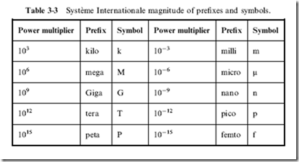
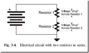
image

image

thousands of units are given the prefix ‘‘k’’, so a resistor having a value of 10,000 ohms is usually referred to as having a value of ‘‘10 kohms’’, or most popularly ‘‘10 k’’.

Looking at more complex circuits, such as the two resistor ‘‘series’’ circuit

shown in Fig. 3-4, you must remember that individual measurements must be taken across each resistor’s two terminals; you do NOT make measurements relative to a common point. The reason for making this statement is to point out that the voltage across a resistor, which is also known as the ‘‘voltage drop’’, is dependent on the current flowing through it.

Using this knowledge, you can understand how electricity flows through the two series resistors in Fig. 3-4. The voltage applied to the circuit causes current to flow through both of the resistors and the amount of current is equal to the current passing through a single resistor value which is the sum of the two resistors. Knowing this current, and an individual resistor’s value, you can calculate the voltage drop across each one. If you do the calculations, you will discover that the voltage drop across each resistor is equal to the applied voltage.

This may be a bit hard to understand, but go back to the pipe/tap/hose

example and think about the situation where you had a pipe/tape/pipe/tap/ hose. In this case, there would be a pressure drop across the first tap and then another pressure drop across the second tap. This is exactly what happens in Fig. 3-4: some voltage ‘‘drops’’ across Resistor 1 and the rest drops across Resistor 2. The amount of the drop across each resistor is proportional to its value relative to the total resistance in the circuit.

To demonstrate this, consider the case where Resistor 1 in Fig. 3-4 is

5 ohms and Resistor 2 is 8 ohms. Current has to flow through Resistor 1 followed by Resistor 2, which means that the total resistance it experiences is equivalent to the sum of the two resistances (13 ohms). The current through the two resistors could be calculated using Ohm’s law, as voltage applied divided by Resistor 1 plus Resistor 2. The general formula for calculating

equivalent the resistance of a series circuit is the sum of the resistances, which is written out as:

Re = R1 + R2+ .. .

Knowing the resistor values, the voltage drop across each resistor can be calculated as its fraction of the total resistance; the voltage across Resistor 1 would be 5/13ths of the applied voltage while the voltage across Resistor 2 would be 8/13ths of the applied voltage. Dividing the resistor values into the individual resistor voltage drops will yield the same current as dividing the applied voltage by the total resistance of the circuit.

Adding the two resistor voltage drops together, you will see that they total the applied voltage. This is a useful test to remember when you are checking your calculations, to make sure they are correct.

The properties of series resistance circuits are summed up quite well as Kirchoff’s voltage law, which states that ‘‘the sum of the voltage drops in a series circuit is equivalent to the applied voltage and current is the same at all points in the circuit.’’

Along with being able to calculate the amount of current passing through a series resistor circuit and the voltage drop across each resistor, you can also calculate the voltage across each resistor in a parallel resistor circuit like Fig. 3-5 as well as the current through all the resistors. To do this, you have to remember Kirchoff’s current law, which states that ‘‘the sum of the currents through each resistance is equivalent to the total current drawn by the circuit and the voltage drops across each resistor is the same as the applied voltage.’’

With each resistor in parallel, it should be fairly obvious that the voltage drop across each one is the same as the applied voltage, and the current flowing through each one can be calculated using Ohm’s law. It should also
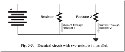
image

be obvious that the current drawn from the power source is equivalent to the sum of the currents passing through each resistor.

If you were to calculate some different current values for different resistances, you would discover that the general formula for the equivalent resistance was:

image

For the simple case of two resistors in parallel, the equivalent resistance can be expressed using the formula:

imageComplex resistor circuits, made up of resistors wired in both series and parallel, like the one shown in Fig. 3-6, can be simplified to a single equivalent resistor by applying the series and resistor formulas that I have presented so far in this section. When doing this, I recommend first finding the equivalent to the series resistances and then the equivalent to the parallel resistances until you are left with one single equivalent resistance.

The last piece of basic electrical theory that I would like to leave you with is how to calculate the power dissipated by a resistor. When you took Newtonian physics, you were told that power was the product of the rate at which something was moving and the force applied to it. In electrical circuits, we have both these quantities, voltage being the force applied to the electrons and current being the rate of movement. To find the power being dissipated (in watts), you can use the simple formula:

P =V x i
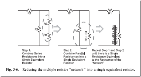
image

or, if you don’t know one of the two input quantities, you can apply Ohm’s law and the formula becomes:

image

I must point out that when you are working with digital electronics, most currents in the circuits are measured somewhere between 100 mA to 20 mA. This seemingly small amount of current minimizes the amount of power that is dissipated (or used) in the digital electronic circuits. I’m pointing this out because if you were to get a book on basic electronics you would dis- cover that the examples and questions will usually involve full amperes of current – not thousands or tens of thousands as I have noted here. The reason why basic electronics books work with full amps is because it is easier for students to do the calculations and they don’t have to worry about working with different orders of magnitude.

So far in these few initial pages of this chapter, I have gone through the same amount of material that is presented in multiple courses in electrical theory. Much of the background material has been left out as well as derivations of the various formulas. For the purposes of working with digital electronics, you should be familiar with the following concepts:

1. Electricity flows like water in a closed circuit.

2. The amount of current flow in a circuit is proportional to the amount of resistance it encounters.

3. Voltage across a load or resistance is measured at its two terminals.

4. Voltage is current times resistance (Ohm’s law).

5. Power is simply voltage times current in a DC circuit.

The other rules are derivations of these basic concepts and while I don’t recommend trying to work them out in an exam, what you do remember can be checked against the basic concepts listed above.

Capacitors

When working with digital electronic circuits, it is very important for you to understand the purpose and operation of the capacitor. Many people shy away from working at understanding the role of capacitors in digital electronics because the formulas that define their response to an applied

voltage do not seem to be intuitive and many of them are quite complex. Further reducing the attractiveness of understanding capacitors is that they do not seem to be a basic component of digital electronics, and when they are used their value and wiring seems to be simply specified by a datasheet or an application note. I must confess that these criteria used to apply to me and I never understood the importance of capacitors in digital electronics until I was reviewing failure analysis of a 4 MB memory chip. As I will show, a dynamic RAM memory element (along with a MOSFET transistor) is essentially a capacitor, and the failure analysis of the chips showed how the differences in these capacitors affected their operation. One of the major conclusions of the failure analysis was that the memory chip wasn’t so much a digital electronic device as a massive array of four million capacitors. This example is meant to show the importance of understanding the operation of capacitors and how they influence digital electronic circuits – being comfortable with the information in this section is more than good enough to use and successfully specify capacitors in digital electronic circuits.

The capacitor itself is a very simple energy storage device; two metal plates (as shown in the leftmost capacitor symbol in Fig. 3-7) are physically separated by a ‘‘dielectric’’ which prevents current from flowing between them. The dielectric is an insulator (‘‘dielectric’’ is a synonym for ‘‘insulator’’) material which enhances the metal plates’ ability to store an electric charge.

The capacitor is specified by the amount of charge it is able to store. The mount of charge stored in a capacitor (which has the symbol ‘‘C’’) is measured in ‘‘farads’’ which are ‘‘coulombs’’ per volt. One coulomb of electrons is a very large number (roughly 6.2 x 10¹⁸) and you will find that for the most part you will only be working with capacitors that can store a very small fraction of a coulomb of electrons.

Knowing that farads are in the units of coulombs per volt, you can find the amount of charge (which has the symbol ‘‘Q’’) in a capacitor by using the formula:
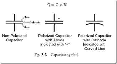
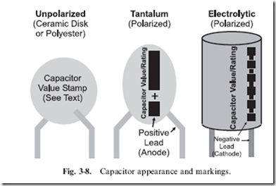
image

image

The fraction of a coulomb that is stored in a capacitor is so small, that the most popularly used capacitors are rated in millionth’s (‘‘microfarads’’ or ‘‘mF’’) or trillionth’s (‘‘picofarads’’ or ‘‘pF’’) of farads. Microfarads are commonly referred to as ‘‘mikes’’ and picofarads are often known by the term ‘‘puffs’’. Using standard materials (such as mica, polyester and ceramics), it is possible to build capacitors of a reasonable size of 1 microfarad (one millionth of a farad) but more exotic materials are required for larger value capacitors. For larger capacitors, the dielectric is often a liquid and the capacitor must be wired according to parameter markings stamped on it, as I have indicated in Fig. 3-8. These are known as ‘‘polarized’’ capacitors and either a ‘‘þ’’ marking or a curved plate (as shown in Fig. 3-7) is used to indicate how the capacitor is wired in the schematic. Like other polarized components, the positive connection is called an ‘‘anode’’ and the negative a ‘‘cathode’’. Along with the markings, you should remember that the anode of a polarized two lead component is always longer than the cathode. The different lead lengths allow automated assembly equipment to distinguish between the two leads and determine the component’s polarity.

Capacitors have two primary purposes in digital electronic circuits. The first is as a voltage ‘‘filter’’ (Fig. 3-9), reducing ‘‘spikes’’ and other problems on a wire carrying current. This use is similar to the use of a water tower in a city; the water tower is filled due to the pressure of the water being pumped into the community. Water is continually pumped to both houses and the water tower, but in times of high usage (like during the day when people are watering their lawns and washing their cars), water from the tower supplements the pumped water to keep the pressure constant. During the
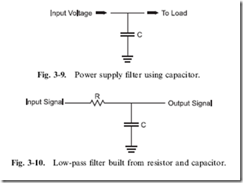
image

night, when few people are using water, the pumped water is stored in the water tower, in preparation for the next day’s requirements.

When you look at digital electronic circuits, you will see two types of capacitors used for power filtering. At the connectors to the power supply, you will see a high value capacitor (10 mF or more) filtering out any ‘‘ripples’’ or ‘‘spikes’’ from the incoming power. ‘‘Decoupling’’ capacitors of 0.047 mF to 0.1 mF are placed close to the digital electronic chips to eliminate small spikes caused when the gates within the chips change state.

Large capacitors will filter out low-frequency (long-duration) problems on the power line while the small capacitors will filter out high-frequency (short- duration) spikes on the power line. The combination of the two will keep the power line ‘‘clean’’ and constant, regardless of the changes in current demand from the chips in the circuit.

The capacitor’s ability to filter signals is based on its ability to accept or lose charge when the voltage across it changes. This capability allows voltage signals to be transformed using nothing more than a resistor and a capacitor, as in the ‘‘low-pass filter’’ shown in Fig. 3-10. This circuit is known as a low-pass filter because it will pass low-frequency alternating current signals more readily than high-frequency alternating current signals.

In digital electronics, we are not so much concerned with how a capacitor affects an alternating current as how it affects a changing direct current.

Figure 3-11 shows the response, across Fig. 3-10’s low-pass filter’s capacitor and resistor, to a digital signal that starts off with a low voltage ‘‘steps’’ up to ‘‘V’’ and then has a falling step back to 0 V.

In Fig. 3-11, I have listed formulas defining the voltage response across the resistor and capacitor to the rising and falling step inputs. These formulas are
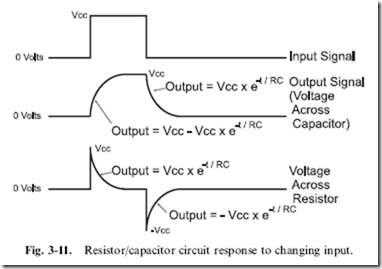
image

found within introductory college electricity courses by knowing that the voltage across the capacitor can be defined by using the formula:

image

which simply states that the voltage across a capacitor at some point in time is a function of the charge within the capacitor at that point of time. The charge within the capacitor is supplied by the current passing through the resistor and the resistor limits the amount of current that can pass through it. As the voltage in the capacitor increases, the voltage across the resistor falls and as the voltage across the resistor falls, the amount of current that is available to charge the capacitor falls. It is a good exercise in calculus to derive these formulas, but understanding how this derivation works is not necessary for working with digital electronics.

There are two things I want to bring out from the discussion of low-pass filters. The first is that the response of the low-pass filter is a function of the product of the resistance and capacitance in the circuit. This product is known as the ‘‘RC time constant’’ and is given the Greek letter ‘‘tau’’ (r) as its symbol. Looking at the formulas, you should see that by increasing the value of r (either by using a larger value resistor or capacitor) the response time of the low-pass filter is increased.

This has two ramifications for digital electronics. The first should be obvious: to minimize the time signals take to pass between gates, the resistance and capacitance of the connection should be minimized. The second is more subtle: the resistor–capacitor response can be used to delay a signal in a circuit. This second issue with resistor–capacitor circuits is actually

very useful in digital electronics for a number of different applications that I will discuss later in the book.

This is a very short introduction to capacitors and their operation in (digital) electronic circuits. Before going on, I would like to reinforce what I’ve said about their importance and recommend that you follow up this section’s material by working through a book devoted to analog electronics.

Semiconductor Operation

Over the past 100 years, we have refined our ability to control the electrical properties of materials in ways that have made radios, TVs and, of course, digital electronic circuits possible. These materials have the ability to change their conductance, allowing current to pass through them under varying conditions. This ability to change from being an insulator to a conductor has resulted in these materials being called ‘‘semiconductors’’, and without them many of the basic devices we take for granted would be impossible.

The most basic electronic semiconductor device is the ‘‘diode’’. The electrical symbol and a sketch of the actual part is shown in Fig. 3-12. Diodes are a ‘‘one-way’’ switch for electricity; current will pass easily in one direction and not in the other. If you were to cut a silicon diode in half and look at its operation at a molecular level, you would see that one-half of the silicon was ‘‘doped’’ (infused with atoms) with an element which can easily give up electrons, which is known as an ‘‘N-type’’ semiconductor. On the other side of the diode, the silicon has been doped with an element that can easily accept electrons, a ‘‘P-type’’ semiconductor.
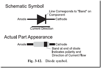
image

image

When a voltage is applied to the diode, causing electrons to travel from the atoms of the N-type semiconductor to the atoms of the P-type, the electrons ‘‘fall’’ in energy from their orbits in the N-type to the accepting orbit spaces in the P-type, as shown in Fig. 3-13. This drop in energy by the electron is accompanied by a release in energy by the atoms in the form of photons. The ‘‘quanta’’ of photon energy released is specific to the materials used in the diode – for silicon diodes, the photons are in the far infrared.

The voltage polarity applied to the diode is known as ‘‘bias’’. When the voltage is applied in the direction the diode conducts in, it is known as ‘‘forward biased’’. As you might expect, when the voltage is applied in the direction the diode blocks current flow, it is known as ‘‘reverse biased’’. This is an important point to remember, both for communicating with others about your designs and for understanding the operation of transistors, as explained below.

To keep the thermodynamic books balanced, the release in energy in terms of photons is accompanied by a corresponding voltage drop across the diode. For silicon diodes, this drop is normally 0.7 volts. The power equation I gave earlier (P ¼ V x i) applies to diodes. When large currents are passed through the diode and this is multiplied by 0.7 V, quite a bit of power can be dissipated within the diode.

If voltage is applied in the opposite direction (i.e. injecting electrons into the P-type side of the diode), the electrons normally do not have enough energy to rise up the slope and leave the orbits of the P-type atoms and enter the electron-filled orbits of the N-type atoms. If enough voltage is applied, the diode will ‘‘break down’’ and electrons will jump up the energy slope. The break down voltage for a typical silicon diode is 100 V or more – it is quite substantial.
image

A typical use for a diode is to ‘‘rectify’’ AC to DC, as shown in Fig. 3-14, in which a positive and negative alternating current is converted using the four diodes to a ‘‘lobed’’ positive voltage signal, which can be filtered using capacitors, as discussed in the previous section.

Along with the simple silicon diode discussed above, there are two other types of diodes that you should be aware of. The first is the ‘‘Zener’’ diode which will break down at a low, predetermined voltage. The typical uses for the Zener diode is for accurate voltage references (Zener diodes are typically built with 1% tolerances) or for low-current power supplies like the one shown in Fig. 3-15. The symbol for the Zener diode is the diode symbol with the bent current bar shown in Fig. 3-15.

Building a power supply using this circuit is actually quite simple: the Zener diode’s break down voltage rating will be the ‘‘regulated output’’ and the ‘‘voltage input’’ should be something greater than it. The value of the current limiting resistor is specified by the formula

image

where ‘‘iapp’’ is the current expected to be drawn (plus a couple of tens of percent margin). The power rating of the Zener diode should take into account the power dissipated if iapp was passing through it.

As I will discuss later in this chapter, there are a lot of inexpensive power regulators that are a lot more efficient than the Zener diode one shown in Fig. 3-15. If you do the math for a typical application (say 9 volts in,

5.1 volt Zener diode and a 20 mA current draw), you will find that at best it is 60% efficient (which is to say 60% of the power drawn by the Zener regulator

circuit and the application is passed to the application, and can often be as low as 25%). The reason for using the Zener diode regulator is its low cost, very small form factor and extreme robustness. Most practical applications will use a linear regulator chip.

The other type of diode that I want to mention in this section is one that you are already very familiar with – the light-emitting diode or LED. As its name implies, this diode emits light (like a light bulb) when a current passes through it. In Fig. 3-16, note that the LED symbol is the same as the diode’s symbol, but with light rays coming from it. The most common package for the LED is also shown in Fig. 3-16 and it consists of a rounded cylinder (somewhat like ‘‘R2D2’’ from Star Wars) with a raised edge at its base with one side flattened to indicate the LED’s cathode (negative voltage connection).

There are a few points that you should be aware of with regard to LEDs. In the past few years, LEDs producing virtually every color of the rainbow (including white) have become available. I must point out that LEDs can only produce one color because of the chemistry of the semiconductors used to build them. You may see advertisements for two or three color LEDs, but these devices consist of two or three LEDs placed in the same plastic package and wired so that when current passes through its pins in a certain direction, a specific LED turns on.
image

The brightness of a LED cannot be controlled reliably by varying the current passing through it, as you would with a light bulb. LEDs are designed to provide a set amount of light with current usually in the range of 5 to 10 mA. Reducing the current below 5 mA may dim its output or it may turn it off completely. A much better way to dim a LED is to use ‘‘pulse wave modulation’’ (PWM), in which the current being passed to the LED is turned on, and faster than the human eye can perceive, with varying amounts of on and off time to set the LED’s brightness. I will discuss PWMs later in the book.

Finally, when I first introduced diodes, I noted that silicon diodes output photons of light in the far infrared and have a 0.7 volt drop when current passes through them. To produce visible light, LEDs are not made out of silicon, they are made from other semiconductor materials in which the energy drop from the N-type semiconductor to the P-type semiconductor produces light in the visible spectrum. This change in material means that LEDs do not have silicon’s 0.7 V drop; instead, they typically have a 2.0 V drop. This is an important point because it will affect the value of the current limiting resistor that you put in series to make sure the LED’s current limit rating is not exceeded or that it does not allow too much current in the circuit to pass through it, resulting in an unnecessary current drain.

It is always a source of amazement to me how many people do not understand how transistors work. For the rest of this section, I will introduce you to the two most common types of transistors and explain how they work as well as what applications they are best suited for. Understanding the characteristics of the two types of transistors is critical to understanding how digital logic is implemented and how you can interface it to different technologies.

As I explain the operation of the ‘‘bipolar’’ transistor, I will endeavor to keep to the ‘‘high level’’ and avoid trying to explain transistor operation using tools like the ‘‘small signal model’’, which is intimidating and obfuscates the actual operation of the device. Instead, I want to introduce you straight to the ‘‘NPN bipolar transistor’’ by its symbol and typical package and pinout for a small scale (low-power) device in Fig. 3-17.

As you have probably heard, a bipolar transistor can be considered a simple switch or a voltage amplifier, but you are probably mistaken on how it is controlled and how it actually works. The transistor is not voltage controlled (as you may have been led to expect); it is actually current controlled. The amount of current passing through the ‘‘base’’ to the ‘‘emitter’’ controls the amount of current that can pass from the ‘‘collector’’ to the emitter. The amount of current that can be passed through the collector is a multiple (called ‘‘beta’’ and given the symbol ‘‘fJ’’ or hFE) of the
image

current flowing through the base; the bipolar transistor is actually an amplifier – a small amount of current allows a greater amount to flow. The simple formulas for the relationship between the base and collector currents are listed in Fig. 3-17.

I must point out that these formulas apply while the maximum collector current is in the ‘‘small signal’’ or ‘‘linear’’ operating range. As a physical device, a transistor can only allow so much current to flow through it; as it reaches this limit, increases in the transistor’s base current will not result in a proportional increase in collector current. This operating region is known as the ‘‘non-linear’’ or ‘‘saturation’’ region and what happens in this situation can be easily understood by looking at what happens in a cross section of a transistor (Fig. 3-18).

A bipolar transistor consists of a P-type semiconductor sandwiched between two N-type semiconductors. This structure forms a reverse biased diode and no current can flow through it. With no current being injected into the NPN bipolar transistor, the P-type semiconductor is known as the ‘‘depletion region’’ because it does not have any electrons. When current is passed to the device, electrons are drawn through the P-type semiconductor via the emitter N-type semiconductor. As electrons are drawn into the P-type semiconductor, the properties of the P-type semiconductor change and take on the characteristics of the N-type semiconductors surrounding it and becomes known as the ‘‘conduction region’’. The more electrons that are drawn from the P-type semiconductor, the larger the conduction region bridging the two pieces of N-type semiconductor and the greater amount of current that can pass from the collector to the emitter. As more electrons are
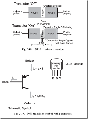
image

drawn from the P-type semiconductor, the conduction region grows until the entire P-type semiconductor of the transistor becomes ‘‘saturated’’.

The PNP bipolar transistor (Fig. 3-19) operates in the complete opposite way to the NPN transistor. It is built from an N-type semiconductor between two P-type semiconductors and to create a conduction region, electrons are injected into the base instead of being withdrawn, as in the case of the NPN bipolar transistor. As in the NPN bipolar transistor, the amount of collector current is a multiple of the base current (and that multiple is also called f3 or hFE).
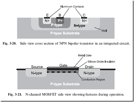
image

Bipolar transistor hFE values can range anywhere from 50 to 500 and the amount of collector current they can handle ranges from a few tens of milliamps to tens of amps. As well as discrete (single) devices being inexpensive, they respond to changes in inputs in extremely short time intervals. You may think they are perfect for use in digital electronics, but they have two faults that make them less than desirable. First, the base current is actually a source of power dissipation in the device, which is usually not an issue when single transistors are used, but is of major concern when thousands or millions are used together in a highly complex digital electronic system.

Secondly, they take up a lot of chip ‘‘real estate’’ and are very expensive to manufacture. Figure 3.20 shows the side view of an NPN bipolar transistor

built on a silicon chip. Instead of butting together different types of semiconductor, it is manufactured as a series of ‘‘wells’’, which are doped with the chemicals to produce the desired type of semiconductor by repeated operations. As many as 35 process steps are required to produce a bipolar transistor.

The N-channel enhancement ‘‘metal oxide silicon field effect transistor’’ (MOSFET) does not have these faults – it is built using a much simpler process (the side view of the transistor is shown in Fig. 3-21) that only requires one doping of the base silicon along with the same bonding of aluminum contacts as the bipolar transistor. N-channel MOSFETs (as they are most popularly known) require nine manufacturing processes and take a fraction of the chip real estate used by bipolar transistors.

The N-channel MOSFET is not a current-controlled device, like the bipolar transistor, but a voltage-controlled one. To ‘‘turn on’’ the MOSFET

(allow current to flow from the ‘‘source’’ to the ‘‘drain’’ pins), a voltage is applied to the ‘‘gate’’. The gate is a metal plate separated from the P-type silicon semiconductor substrate by a layer of silicon dioxide (most popularly known as ‘‘glass’’). When there is no voltage applied to the gate, the P-type silicon substrate forms a reverse biased diode and does not allow current flow from the source to the drain. When a positive voltage is applied to the gate of the N-channel MOSFET, electrons are drawn to the substrate immediately beneath it, forming a temporary N-type semiconductor ‘‘conduction region’’, which provides a low-resistance path from the source to the drain. MOSFET transistors are normally characterized by the amount of current that can pass from the source to the drain along with the resistance of the source/drain current path.

The symbol for the N-channel MOSFET, along with its complementary device, the P-channel MOSFET are shown in Fig. 3-22. The P-channel MOSFET creates a conduction region when a negative voltage is applied to its gate. MOSFET transistors come in a variety of packages and some can handle tens of amps of current, but they tend to be very expensive.

MOSFETs do not have the issues of bipolar transistors; their gate widths (the measurement used to characterize the size of MOSFET devices) are, at the time of this writing, as small as 57 nm in high-performance micro- processors and memory chips. The voltage-controlled operation of MOSFETs eliminates the wasted current and power of the bipolar transistor’s base, but while MOSFETs do not have the disadvantages of bipolar transistors, they do not have their advantages.

MOSFET transistors do not have a small signal/linear operating region;t hey tend to change from completely off to completely on (conducting) with a
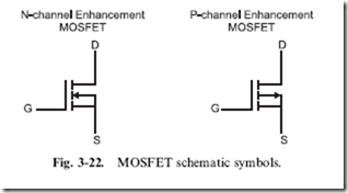
image

very small intermediate range. MOSFETs also tend to operate at slower speeds than bipolar devices because the gates become capacitors and ‘‘slow down’’ the signals, as I showed in the previous section. This point has become somewhat moot as modern MOSFET designs are continually increasing in speed, providing us with extremely high-speed PCs and other electronic devices. Finally, it is difficult to manufacture MOSFETs with high current capabilities; while high current MOSFETs are available, they are surprisingly expensive.
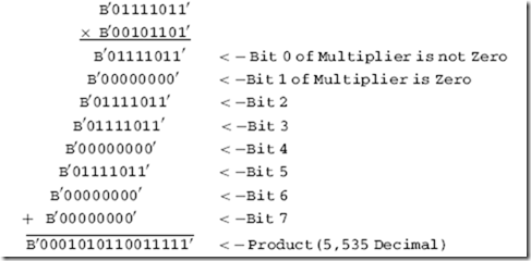
The characteristics of the two types of transistors give way to the conclusion that bipolar transistors are best suited to situations where a few high current devices are required. MOSFET transistors are best suited for applications where large numbers of transistors are placed on a single chip. Today, for the most part, digital electronic designs follow these guidelines, but we are left with an interesting legacy. Despite being much simpler structurally and cheaper to manufacture, MOSFET transistors were only perfected in the late 1960s, whereas bipolar technology had already been around for 20 years and it was able to become entrenched as the basis for many digital electronic devices and chips. For this reason, you must be cognizant of the operating characteristics of bipolar transistors as well as those of MOSFET transistors. In the next section, many of these differences will become apparent.