8086 Interrupts , Predefined Interrupts , Internal Interrupts , External Maskable Interrupts , Interrupt Procedures , Interrupt Priorities , Interrupt Pointer Table and 8086 DMA

9.10 8086 Interrupts

The 8086 assigns every interrupt a type code so that the 8086 can identify it. Interrupts can be initiated by external devices or internally by software instructions or by exceptional conditions such as attempting to divide by zero.

9.10.1 Predefined Interrupts

The first five interrupt types are reserved for specific functions.

image

The interrupt vectors for these five interrupts are predefined by Intel. The user must provide the desired IP and CS values in the interrupt pointer table. The user may also initiate these interrupts through hardware or software. If a predefined interrupt is not used in a system, the user may assign some other function to the associated type.

The 8086 is automatically interrupted whenever a division by zero is attempted.

This interrupt is nonmaskable and is implemented by Intel as part of the execution of the divide instruction.

When the TF (trap flag) is set by an instruction, the 8086 goes into single-step mode. The TF can be cleared to zero as follows:

imageNote here that O[BP] rather than [BP] is used because BP cannot normally be used without displacement in the 8086 assembler. Now, to set TF, the AND instruction just shown should be replaced by OR 0 [BP],OlOOH. Once TF is set to 1, the 8086 automatically generates a type 1 interrupt after execution of each instruction. The user can write a service routine at the interrupt address vector to display memory locations and/or register to debug a program. Single-step mode is nonmaskable and cannot be enabled by the STI (enable interrupt) or disabled by the CLI (disable interrupt) instruction.

The nonmaskable interrupt is initiated via the 8086 NMI pin. It is edge triggered (LOW to HIGH) and must be active for two clock cycles to guarantee recognition. It is normally used for catastrophic failures such as a power failure. The 8086 obtains the interrupt vector address by automatically executing the INT2 (type 2) instruction internally.

The type 3 interrupt is used for breakpoints and is nonmaskab1e. The user inserts the 1-byte instruction INT3 into a program by replacing an instruction. Breakpoints are useful for program debugging.

The interrupt on overflow is a type 4 interrupt. This interrupt occurs if the overflow flag (OF) is set and the INTO instruction is executed. The overflow flag is affected, for example, after execution of a signed arithmetic (such as IMUL, signed multiplication) instruction. The user can execute an INTO instruction after the IMUL. If there is an overflow, an error service routine written by the user at the type 4 interrupt address vector is executed.

9.10.2 Internal Interrupts

The user can generate an interrupt by executing an interrupt instruction INTnn. The INTnn instruction is not maskable by the interrupt enable flag (IF). The INTnn instruction can be used to test an interrupt service routine for external interrupts. Type codes 32-255 can be used; type codes 5 through 31 are reserved by the Intel for future use. If a predefined interrupt is not used in a system, the associate type code can be utilized with the INTnn instruction to generate software (internal) interrupts.

9.10.3 External Maskable Interrupts

The 8086 maskable interrupts are initiated via the INTR pin. These interrupts can be enabled or disabled by STI (IF= 1) or CLI (IF= 0), respectively. IfiF = 1 and INTR active (HIGH) without occurrence of any other interrupts, the 8086, after completing the current instruction, generates INTA LOW twice, each time for about one cycle.

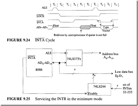
INTA is only generated by the 8086 in response to INTR, as shown in Figure M9.24. The interrupt acknowledge sequence includes two INTA cycles separated by two clock cycles. ALE is also generated by the 8086 and will load the address latches with indeterminate information. The first INTA bus cycle indicates that an interrupt acknowledge cycle is in progress and allows the system to be ready to place the interrupt type code on the next INTA bus cycle. The 8086 does not obtain the information from the bus during the first cycle. The external hardware must place the type code on the lower half of the 16-bit data bus (D0-D7) during the second cycle.

In the minimum mode, the M/IO is LOW, indicating I/O operation during theINTA bus cycles. The 8086 internal LOCK signal is also LOW from T2 of the first bus cycle until T2 of the second bus cycle to keep the BIU from accepting a hold request between the two INTA cycles. Figure 9.25 shows a simplified interconnection between the 8086 and 74LS244 for servicing the INTR. INTA enables the 74LS244 to place type code nn on the 8086 data bus. In the maximum mode, the status lines S0-S2 will generate the INTA output.

9.10.4 Interrupt Procedures

Once the 8086 has the interrupt type code (via the bus for hardware interrupts, from software interrupt instructions INTnn, or from the predefined interrupts), the type code is multiplied by 4 to obtain the corresponding interrupt vector in the interrupt vector table. The 4 bytes of the interrupt vector are the least significant byte of the instruction pointer, the most significant byte of the instruction pointer, the least significant byte of the code segment register, and the most significant byte of the code segment register. During the transfer of control, the 8086 pushes the flags and current code segment register and instruction pointer onto the stack. The new CS and IP values are loaded. Flags TF and IF are then cleared to zero. The CS and IP values are read by the 8086 from the interrupt vector table. No segment registers are used when accessing the interrupt pointer table. S4 S3 has the value 102 to indicate no segment register selection.

9.10.5 Interrupt Priorities

As far as the 8086 interrupt priorities are concerned, the single-step interrupt has the highest priority, followed by NMI, followed by the software interrupts. This means that a

image

simultaneous NMI and single-step interrupt will cause the NMI service routine to follow the single step; a simultaneous software interrupt and single step interrupt will cause the software interrupt service routine to follow the single step; and a simultaneous NMI and software interrupt will cause the NMI service routine to be executed prior to the software interrupt service routine. The INTR is maskable and has the lowest priority. A priority interrupt controller such as the 8259A can be used with the 8086 INTR to provide eight levels of interrupts. The 8259A has built-in features for expansion of up to 64levels with additional 8259s. The 8259A is programmable and can be readily used with the 8086 to obtain multiple interrupts from the single 8086 INTR pin.

9.10.6 Interrupt Pointer Table

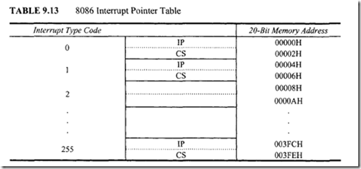
The interrupt pointer table provides interrupt address vectors (IP and CS contents) for all the interrupts. There may be up to 256 entries for the 256 type codes. Each entry consists of two addresses, one for storing IP and the other for storing CS. Note that in the 8086 each interrupt address vector is a 20-bit address obtained from IP and CS.

To service an interrupt, the 8086 calculates the two addresses in the pointer table where IP and CS are stored for a particular interrupt type as follows:

image

The table address for IP = 4 x nn and the table address for CS = 4 x nn + 2. For example, consider INT2:

Address for IP = 4 x 2 = 00008H

Address for CS = 00008 + 2 = 0000AH

The values ofiP and CS are loaded from location 00008H and OOOOAH in the pointer table. Similarly, the IP and CS addresses for other INTnn are calculated, and their values are obtained from the contents of these addresses in the pointer table (Table 9.13). The 8086 interrupt vectors are defined as follows:

image

Interrupt service routines should be terminated with an IRET (interrupt return) instruction, which pops the top three stack words into the IP, CS, and flags, thus returning control to the right place in the main program.

9.12 8086 DMA

When configured in minimum mode (MN/MX HIGH) the 8086 provides HOLD and HLDA (hold acknowledge) signals to control the system bus for DMA applications. In this type ofDMA, the peripheral device can request the DMA transfer via the DMA request (DRQ) line connected to a DMA controller chip such as the 8257. In response to this request, the 8257 sends a HOLD signal to the 8086. The 8257 then waits for the HLDA signal from the 8086. On receipt of this HLDA, the 8257 sends a DMACK signal to the peripheral device. The 8257 then takes over the bus and controls data transfer between the RAM and peripheral device. On completion of data transfer, the 8257 returns control to the 8086 by disabling the HOLD and DMACK signals.

image

Example 9.21

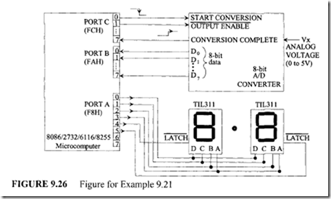
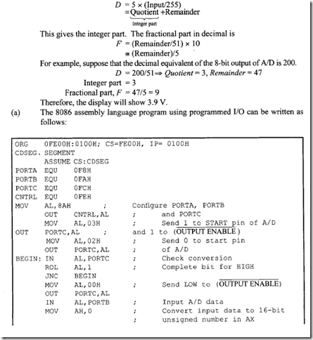
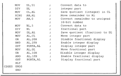
In Figure 9.26, an 8086-based microcomputer is required to implement a voltmeter to measure voltage in the range 0 to 5 V and display the result in two decimal digits: one integer part and one fractional part. The microcomputer is required to start the AID converter at the falling edge of a pulse via bit 0 of Port C. When the conversion is completed, the A/D’s "conversion complete" signal will go HIGH. During the conversion, the AID’s "conversion complete" signal stays LOW. Use the 8255 control register= FEH, Port A= F8H, Port B = FAH, and Port C = FCH.

Using programmed I/O, the microcomputer is required to poll the AID’s "conversion complete" signal. When the conversion is completed, the microcomputer will send a LOW of the AID converter’s "output enable" line via bit 1 to port C and then input the 8-bit output from AID via port B and display the voltage (0 to 5 V) in two decimal digits (one integer and one fractional) via port A on two TIL 311 displays. Note that the TIL 311 has an on-chip BCD to seven-segment decoder. The microcomputer will output each decimal digit on the common lines (bits 0-3 of port A) connected to the DCBA inputs of the displays. Each display will be enabled by outputting LOW on each LATCH line

image

in sequence (one after another) so that the input voltage Vx (0 to 5 V) will be displayed with one integer part and fractional part. Write an 8086 assembly language program to accomplish this.

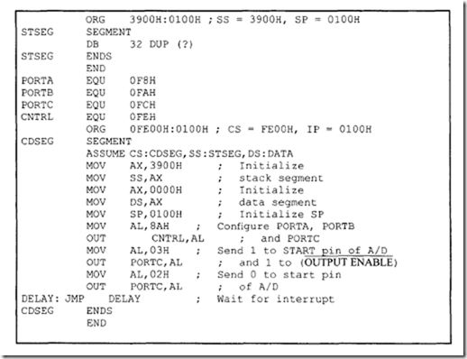
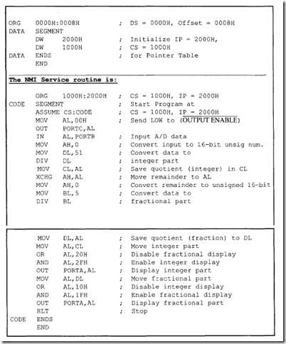
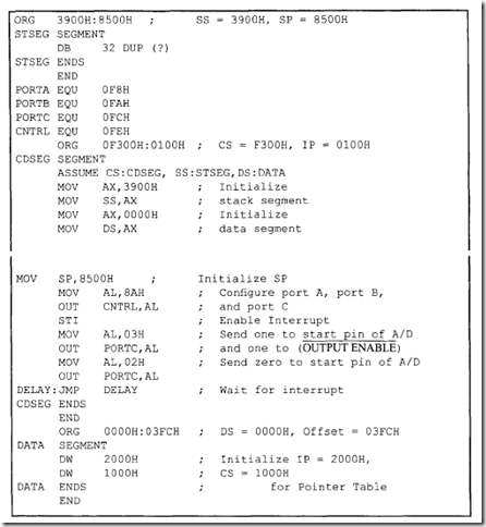
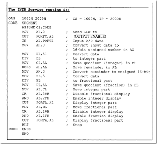
Using interrupt I/O (both NMI and INTR), repeat the task. Write the main program to initialize the 8255 control register and start the A/D. The service routine will input the AID data, display the result, and stop. Write an 8086 assembly language program for the main program and the service routine. Use the memory map of your choice. Write the service routines for both NMI and INTR starting at IP=2000H, CS=1000H. Use 8086 assembler directive such as ORG CS:IP for the HP (Hewlett-Packard) 64XXX microcomputer development system in the following programs.

Solution

Because the maximum decimal value that can be accommodated in 8 bits is 255 10 (FF16), the maximum voltage of 5 V will be equivalent to 25510• This means the display in decimal is given by

image

image

(b) UsingNMI

In Figure 9.26, connect the "conversion complete" to 8086 NMI; all other connections in Figure 9.26 will remain unchanged. Note that all addresses selectable by the user are arbitrarily chosen in the following. The main program in 8086 assembly language is

image

image

(c) Using INTR

All connections in Figure 9.26 will be same except AID’s "conversion complete" to 8086 INTR as shown in Figure 9.27. All other connections in Figure 9.26 will remain unchanged. INT FFH is used. In response to INTR, the 8086 pushes IP and SR onto the stack, and generates LOW on INTA. An octal buffer such as 74LS244 can be enabled by this INTA to transfer FF 16 in this case (can be entered via eight DIP switches connected to+ 5 V through a I KQ resistor) to the input of the octal buffer. The output of the octal buffer is connected to the demultiplexed D0-D7 lines of the 8086. The 8086 executes INT FFH and goes to the interrupt pointer table to load the contents of physical addresses 003FCH (logical address:

CS = OOOOH, IP = 03FCH) and 003FEH (logical address: CS = OOOOH, IP = 03FEH) to obtain IP and CS for the service routine respectively. Suppose that it is desired to write the service routine at IP = 2000H and CS = 1 OOOH; these IP and CS values must be stored at addresses 003FCH and 003FEH respectively. All user selectable addresses are arbitrarily chosen. The main program in 8086 assembly language is

image

image


System Desi :n Usin : the 8086 , 8086 Pins and Signals , Clock Generation Signals , Ready Signals , Basic 8086 System Concepts , 8086 Bus Cycle and Address and Data Bus Concepts .

9.9 System Desi :n Usin : the 8086

This section covers the basic concepts associated with interfacing the 8086 with its support chips such as memory and I/O . Topics such as timing diagrams and 8086 pins and signals will also be included. Appendix E provides data sheets for Intel 8086 and support chips.

9.9.1 8086 Pins and Signals

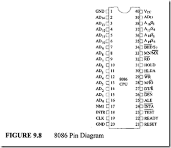
The 8086 pins and signals are shown in Figure 9.8. As mentioned before, the 8086 can operate in two modes. These are the minimum (uniprocessor systems with a single 8086) and maximum mode (multiprocessor system with more than one 8086). MN/MX is an input pin used to select one of these modes.

When MN/MX is HIGH, the 8086 operates in the minimum mode. In this mode, the 8086
image

is configured (that is, pins are defined) to support small single-processor systems using a few devices that use the system bus. When MN/MX is low, the 8086 is configured (that is, some of the pins are redefined in maximum mode) to support multiprocessor systems. In this case, the Intel 8288 bus controller is added to the 8086 to provide bus control and compatibility with the multibus architecture. Note that, in a particular application, MN/ MX must be tied to either HIGH or LOW.

The AD0-AD15 lines are a 16-bit multiplexed address/data bus. During the first clock cycle, AD0-AD15 are the low-order 16-bit address. The 8086 has a total of20 address lines. The upper four lines, A 16/S3, A 17/S4, A 18/S5, and A 1c/S6, are multiplexed with the status signals for the 8086. During the first clock period of a bus cycle (read or write

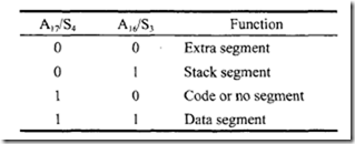
cycle), the entire 20-bit address is available on these lines. During all other cycles for memory and I/O , AD0-AD15 lines contain the 16-bit data, and the multiplexed address I status lines become S3, S4 , S5, and S6• S3 and S4 are decoded as follows:
 

image

Therefore, after the first clock cycle of an instruction execution, the A 17/S4 and A 16/S3 pins specify which segment register generates the segment portion of the 8086 address. Thus, by decoding these pins and then using the decoder outputs as chip selects for memory chips, up to four megabytes (one megabyte per segment) can be included. This provides a degree of protection by preventing erroneous write operations to one segment

from overlapping onto another segment and destroying the information in that segment. A 18/S5 and A 19/S6 are used as A 18 and A 19, respectively, during the first clock cycle of an instruction execution. If an I/O instruction is executed, they stay LOW for the first clock

period. During all other cycles, A 18/S5 indicates the status of the 8086 interrupt enable flag

and A19/S6 becomes S6; a LOW S6 pin indicates that the 8086 is on the bus. During a hold acknowledge clock period, the 8086 tristates the A 19/S6 pin and this allows another bus master to take control of the system bus. The 8086 tristates AD0-AD15 during interrupt acknowledge or hold acknowledge cycles.

clip_image003BHE/S 7 is used as BHE (bus high enable) during the first clock cycle of an instruction execution. The 8086 outputs a LOW on this pin during the read, write, and interrupt acknowledge cycles in which data are to be transferred in a high-order byte (AD15-AD8) of the data bus. BHE can be used in conjunction with AD0 to select memory banks. A thorough discussion is provided later. During all other cycles, BHE/S 7 is used as S7 and the 8086 maintains the output level (BHE) of the first clock cycle on this pin. S7 is the same as BHE and does not have any special meaning.

TEST is an input pin and is only used by the WAIT instruction. The 8086 enters a wait state after execution of theW AIT instruction until a low is seen on the TEST pin. This input is synchronized internally during each clock cycle on the leading edge of the clock.

INTR is the maskable interrupt input. This line is not latched, so INTR must be held at a HIGH level until it is recognized to generate an interrupt.

NMI is the nonmaskable interrupt pin input activated by a positive edge.

RESET is the system reset input signal. This signal must be HIGH for at least four clock cycles to be recognized, except on power-on, which requires a 50-f.!sec reset pulse. It causes the 8086 to initialize registers DS, ES, SS, IP, and flags to zeros. It also initializes CS to FFFFH. Upon removal of the RESET signal from the RESET pin, the 8086 will fetch its next instruction from a 20-bit physical address FFFF0H (CS = FFFFH, IP = 0000H). When the 8086 detects a positive edge of a pulse on RESET, it stops all activities until the signal goes LOW. Upon hardware reset, the 8086 initializes the system as follows:
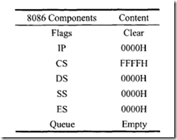
image

As mentioned before, the 8086 can be configured in either minimum or maximum mode using the MN/MX input pin. In minimum mode, the 8086 itself generates all bus control signals. These signals are as follows:

  • DTIR (data transmit/receive) is an output signal required in a minimum system that uses an 8286/8287 data bus transceiver. It is used to control direction of data flow through the transceiver.
  • DEN (data enable) is provided as an output enable for the 8286/8287 in a minimum system that uses the transceiver. DEN is active LOW during each memory and 1/0 access and for INTA cycles.
  • ALE (address latch enable) is an 8086 output signal that can be used to demultiplex the multiplexed 8086 pins including AD0-AD15 into A0-A15 and D0-D15 at the falling edge of ALE.
  • M/IO is an 8086 output signal. It is used to distinguish a memory access (M/IO = HIGH) from an 110 access (M/lO= LOW). When the 8086 executes an 1/0 instruction such as IN or OUT, it outputs a LOW on this pin. On the other hand, the 8086 outputs HIGH on this pin when it executes a memory reference instruction such as MOV AX, [SI].
  • WR is used by the 8086 for a write operation. The 8086 outputs a low on this pin to indicate that the processor is performing a write memory or write I/O operation, depending on the M/IO signal. Similarly, RD is low whenever the 8086 is reading data from memory or an I/O  location.
  • For interrupt acknowledge cycles (for the INTR pin), the 8086 outputs LOW on the INTApin.
  • HOLD (input) and HLDA (output) pins are used for DMA. A HIGH on the HOLD pin indicates that another master is requesting to take over the system bus. The processor receiving the HOLD request will output a HIGH on the HLDA as an acknowledgment. At the same time, the processor tristates the system bus. Upon receipt of LOW on the HOLD pin, the processor places LOW on the HLDA pin and takes over the system bus.
  • CLK (input) provides the basic timing for the 8086 and bus controller.
  • READY (input) pin is used for slow peripheral devices.

There are four versions of the 8086. They are 8086, 8086-1, 8086-2, and 8086-4. There is no difference between the four versions other than the maximum allowed clock speeds. The 8086 can be operated from a maximum clock frequency of 5 MHz. The maximum clock frequencies of the 8086-1, 8086-2 and 8086-4 are 10 MHz, 8 MHz and 4 MHz, respectively. Because the design of these processors incorporates dynamic cells, a minimum frequency of2 MHz is required to retain the state of the machine. The 8086-4, 8086, and 8086-2 will be referred to as 8086 in the following discussion.
image

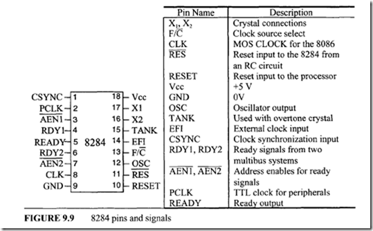
The reset, clock, and the ready signals of the 8086 can be generated by the Intel 8284. Figure 9.9 shows the pins and signals of the 8284.

The 8284 is an 18-pin chip designed for providing three input signals for the 8086:

1. 8086 CLK input

2. 8086 Reset input

3. 8086 Ready input

The 8284 pins and signals are described in the following.

Clock Generation Signals

Because the 8086 has no on-chip clock generator circuitry, the 8284 chip is required to provide the 8086 clock input. The 8284 F/C input pin is provided for clock source selection. When the F/C pin is connected to LOW, a crystal connected between 8284’s X 1 and X2 pins is used. On the other hand, when F/C is connected to HIGH, an external clock source is used; the external clock source is connected to the 8284 EFI (external frequency input) pin. The 8284 divides the clock inputs at the X 1X2 pins or the EFI pin by 3. This means that if a 15-MHz crystal is connected at the X 1X2 or EFI pins, the 8284 CLK output pin will be 5 MHz. The 8284 CLK pin will be connected to the 8086 CLK pin. This provides the clock input for the 8086. When selecting a crystal for use with the 8284, the crystal series resistance should be as low as possible. The oscillator delays in the 8284 appear as inductive elements to the crystal and cause the 8284 to run at a frequency below that of the pure series resonance: a capacitor CL should be placed in series with the crystal and the 8284 X2 pin. The capacitor cancels the inductive element. The impedance of the capacitor Xc = 11(2rcfCJ wherefis the crystal frequency. Intel recommends that the crystal series resistance plus Xc should be kept less than 1 KQ.

As the crystal frequency increases, CL should be decreased. For example, a 12- MHz crystal may require CL = 24 pf whereas a 22-MHz crystal may require CL = 8pf. CL values of 12 to 15 pf may be used with a 15-MHz crystal. Two crystal manufacturers recommended by Intel are Crystle Corp., Model CY 15A (15 MHz), and CTS Knight, Inc., Model CY 24A (24 MHz). Note that the 8284 CLK output pin is the MOS clock for the 8086.

There are two more clock outputs on the 8284, the PCLK (peripheral clock) pin and the OSC (oscillator) clock pin. These signals are provided to drive peripheral ICs. The 8284 divides the frequency of the crystal at the X 1X2 pins or the external clock at the EFI pin by 6 to provide the PCLK. Therefore, the frequency of the PCLK is half the frequency of the 8284 CLK output pin. This means that for a 15-MHz crystal, the PCLK and CLK outputs are 2.5 MHz and 5 MHz respectively. Furthermore, PCLK is provided at the TTL-compatible level rather than at the MOS level. The OSC clock, on the other hand, is derived from the crystal oscillator inside the 8284 and has the same clock frequency as the crystal. Therefore, the OSC output is three times that of the CLK output. The OSC is also TTL compatible. Finally, the CSYNC (clock synchronization) input pin when connected to HIGH provides external synchronization in systems that employ multiple clocks. A typical8284 interface to the 8086 for providing a 5-MHz clock to the 8086 is shown in the following figure:
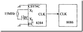
imageReset Signals

When designing the microprocessor’s reset circuit, two types of reset must be considered: power-up reset and manual reset. These reset circuits must be designed using the parameters specified by the manufacturer.

Therefore, a microprocessor must be reset when its Vcc pin is connected to power. This is called "power-up reset." After some time during normal operation the microprocessor can be reset upon activation of a manual switch such as a pushbutton. A reset circuit, therefore, needs to be designed following the timing parameters associated with the microprocessor’s reset input pin specified by the manufacturer. The reset circuit, once designed, is connected to the microprocessor’s reset pin.

As mentioned before, the 8086 reset input provides a hardware mechanism for initializing the 8086 microprocessor. This is typically done at power-up to provide an orderly start-up of the system. The 8284 RES (reset input) pin when driven active LOW generates a HIGH on the 8284 reset output pin. The 8284 reset pin is connected to the 8086 reset (input) pin. As mentioned before, Intel designed the 8086 in such a way that the 8086 requires its reset pin to be HIGH for at least four clock cycles in order to obtain the physical address (FFFFOH) of the first instruction to be executed, except after power-on, which requires a 50-f.Lsec reset pulse.

According to Intel, in order to guarantee a reset from power-up, the 8086 reset input must remain below 1.05 V for 50 f!Sec after Vee has reached the minimum supply voltage of 4.5 V. The 8284 RES input can be driven by an RC circuit as shown in the following figure:

image

The voltage across the capacitor initially is zero upon connecting +Vee to power. If the switch is not depressed, the capacitor charges to +Vee through the resistor after a definite time determined by the time constant RC.

The charging voltage across the capacitor can be determined from the following equation. Capacitor voltage, VcCt) = vee X [1 – exp(-t/RC)], where t =50 f!Sec and VcCt) = 1.05 V, and vee = 4.5 V. Substituting these values in the equation, RC = 188 f!Sec. For example, if Cis chosen to be 0.1 f.LF, then R is 1.88 KQ.

When the switch is depressed, the 8284 RES input pin is short-circuited to ground. This takes the 8284 RES pin to LOW and thus discharges the capacitor. As the switch is released, the direct short to ground is broken. However, the 8284 RES pin remains effectively short-circuited to ground through the discharged capacitor. The capacitor now starts to recharge with time toward the +Vee voltage level.

The 8284 generates a reset signal from an internal Schmitt trigger input. A Schmitt trigger is a special analog circuit that shifts the switching threshold based on whether the input changes from LOW to HIGH or from HIGH to LOW. To illustrate this, consider a TTL Schmitt trigger inverter. Suppose that the input of this inverter is at 0 V (logic 0). The output will be approximately 3.4 V (logic 1). Now, because of the Schmitt trigger circuit, if the input voltage is increased, the output will not go to low until the value is about I.7 V. Also, after reaching a low output, the inverter will not produce a HIGH output until the input is decreased to about 0.9 V. Thus, the switching threshold for positive-going input changes is about 1.7 V and for negative-going input changes is about 0.9 V.

The difference between the two thresholds is called "hysteresis." The Schmitt trigger inverter provides I.7 V – 0.9 V = 0.8 V of hysteresis. Schmitt trigger inputs provide high noise immunity and will normally not respond to the noise encountered in microprocessor systems if its hysteresis is greater than the noise amplitude.

As the voltage across the capacitor increases with time, it remains at logic 0 level as long as the logic 1 threshold of the Schmitt trigger. Thus, the 8284 RES input is maintained at logic 0 for at least four clock cycles so that the 8284 RESET output will apply a HIGH at the 8086 reset input for at least four clock cycles. Note that whenever the 8282 RES input is at logic 0, the reset output pin of the 8284 is switched to logic I according to the timing parameters.

Ready Signals

The 8284 Ready (output) pin is connected to the 8086 Ready (input) pin to insert wait states for slow peripheral devices connected to the 8086. There are two main ways to disable this function when not used. One way is to connect the 8086 Ready pin to HIGH, and keep the 8284 Ready output pin floating. The other way is to connect the 8284 RDYI and RDY2 pins to LOW, and the AENI and AEN2 to HIGH, which will permanently disable this function. The 8284 Ready (output) pin can then be connected to the 8086 Ready input pin.

The RDYl, AENI and RDY2, AEN2 input signals provide logic for operation with multiprocessor systems and the 8284 ready output. In multiprocessor systems, these signals are used to control access over the system bus by several 8086’s. The 8284 TANK pin is replaced by the ASYNC input pin on the newer version of 8284. The ASYNC pin can be driven to LOW by a slower device to generate the 8284 READY output pin which can be connected to the 8086 READY pin. This makes it easier for the slower devices to
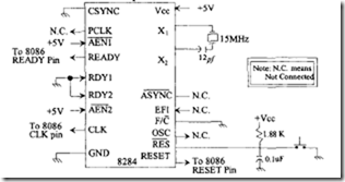
imageinterface to the 8086. Typical8284 clock (using a 15-MHz crystal), reset, and ready signal (unused) connections to single 8086-appropriate pins are shown in the above figure.

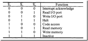
In the maximum mode, some of the 8086 pins in the minimum mode are redefined. For example, pins HOLD, HLDA, WR, M/10, DTJR, DEN, ALE, and INTA in the minimum mode are redefined as RQ/GTO, RQ/GTI, LOCK, Sb s;-, S0, QS0, and QS1 , respectively. In maximum mode, the 8288 bus controller decodes the status information from S0, s;-, and S2 to generate the bus timing and control signals that are required for a bus cycle. S0, S1, and S2 are 8086 outputs and are decoded as follows:
imageThe RQ/GT0 and RQ/GTl request/grant pins are used by other local bus masters to force the processor to release the local bus at the end of the processor’s current bus cycle. Each pin is bidirectional, with RQ/GTO having higher priority than RQ/GTl.These pins have internal pull-up resistors so that they may be left unconnected. The request/grant function of the 8086 works as follows:

  • A pulse (one clock wide) from another local bus master (RQ/GTO or RQ/GTl pin) indicates a local bus request to the 8086.
  • At the end of the current 8086 bus cycle, a pulse (one clock wide) from the 8086 to the requesting master indicates that the 8086 has relinquished the system bus and tristates the outputs. Then the new bus master subsequently relinquishes control of the system bus by sending a LOW on RQ/GTO or RQ/GTl pin. The 8086 then regains bus control.
  • The 8086 outputs LOW on the LOCK pin to prevent other bus masters from gaining control of the system bus.

Note that since the 8086 RESET vector is located at the physical address FFFFOH, there may not be enough locations available to write programs. The following 8086 instructiQn sequence can be used with 8086 assembler (HP 64XXX) to jump to a different code segment upon hardware reset to write programs:

imageThe above instruction sequence will allow the 8086 to jump to the offset START (0200H) in code segment 1000H upon hardware reset where the user can write programs.

9.9.2 Basic 8086 System Concepts

This section describes basic concepts associated with the 8086 bus cycles, address and data bus, in minimum mode.

8086 Bus Cycle

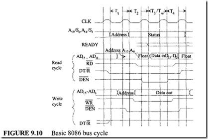
To communicate with external devices via the system for transferring data or fetching instructions, the 8086 executes a bus cycle. The 8086 basic bus cycle timing diagram is shown in Figure 9.10. The minimum bus cycle contains four microprocessor clock periods or four T states. Note that each cycle is called a T state. The bus cycle timing diagram depicted in Figure 9.10 can be described as follows:

1. During the first T state (T1), the 8086 outputs the 20-bit address computed from a segment register and an offset on the multiplexed address/data/status bus.

2. For the second T state (T2), the 8086 removes the address from the bus and either
image

tristates or activates the AD 15-AD0 lines in preparation for reading data via the AD 15-AD0 lines during the T3 cycle. In the case of a write bus cycle, the 8086 outputs data on the AD15-AD0 lines during the T3 cycle. Also, during T2, the upper four multiplexed bus lines switch from address (A19-A16) to bus cycle status (SM S5, S4, S3). The 8086 outputs LOW on RD (for the read cycle) or WR (for the write cycle) during portion ofT2 , all ofT3, and portion ofT4

3. During T3 , the 8086 continues to output status information on the four A 19-A16/ S6-S3 lines and will continue to output write data or input read data to or from the AD 15-AD0 lines.

4. If the selected memory or I/O device is not fast enough to transfer data to the 8086, the memory or I/O device activates the 8086’s READY input line LOW by the start ofT3 • This will force the 8086 to insert additional clock cycles (wait

states TJafter T2 • Bus activity during Tw is the same as that during T3• When the selected device has had sufficient time to complete the transfer, it must activate the 8086 ready pin HIGH. As soon as the Tw clock period ends, the 8086 executes the last bus cycle (T4). The 8086 will latch data on the AD 15-AD0 lines during the last wait state or during T3 if no wait states are requested.

5. During T4 , the 8086 disables the command lines and the selected memory and I/O devices from the bus. Thus, the bus cycle is terminated in T4. The bus cycle appears to devices in the system as an asynchronous event consisting of an address to select the device, a register or memory location within the device, a read strobe, or a write strobe along with data.

6. The DEN and DTIR pins are used by the 8286/8287 transceiver in a minimum system. During the read cycle, the 8086 outputs DEN LOW during part of the T2 and all of the T3 cycles. This signal can be used to enable the 8286/8287 transceiver. The 8086 outputs a LOW on the DT/R pin from the start of the T1 through part of the T4 cycles. The 8086 uses this signal to receive (read) data from the receiver during T3-T4• During a write cycle, the 8086 outputs DEN LOW during part of the T1, all of the T2, and T3, and part of the T4 cycles. The signal can be used to enable the transceiver. The 8086 outputs a HIGH on DT/R throughout the 4 bus cycles to transmit (write) data to the transceiver during T3-T4

image

Address and Data Bus Concepts

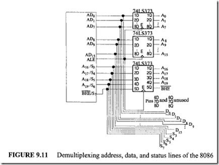
The majority of memory and I/0 chips capable of interfacing to the 8086 require a stable address for the duration of the bus cycle. Therefore, the address on the 8086 multiplexed address/data bus during T1 should be latched. The latched address is then used to select the desired I/0 or memory location. To demultiplex the bus, the 8086 ALE pin can be used along with three 74LS373 latches.

The 74LS373 Output Control (OC) pin can be connected to ground with the 74LS373 pin represented by G or CorLE (shown as E in Figure 9.11) in data book tied to 8086 ALE. This will latch the 8086 address and BHE pins at the falling edge of ALE. Figure 9.11 shows how this can be accomplished.

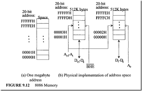
The programmer views the 8086 memory address space as a sequence of one
image

mega bytes in which any byte may contain an 8-bit data element and any two consecutive bytes may contain a 16-bit data element. There is no constraint on byte or word addresses (boundaries). The address space is physically implemented on a 16-bit data bus by dividing the address space into two banks of up to 512K bytes as shown in Figure 9.12. These banks can be selected by BHE and A0 as follows:

imageclip_image003[1]One bank is connected to D7-D0 and contains all even-addressed bytes (A0 = 0). The other bank is connected to D 15-D8 and contains odd-addressed bytes (A0 = 1). A particular byte in each bank is addressed by A 19-A1 • The even-addressed bank is enabled by a LOW on A0, and data bytes are transferred over the DrD0 lines. The 8086 outputs a HIGH on BHE (bus high enable) and thus disables the odd-addressed bank. The 8086 outputs a LOW on BHE to select the odd-addressed bank and a HIGH on A0 to disable the even-addressed bank. This directs the data transfer to the appropriate half of the data bus.

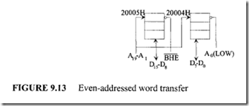
Activation of A0 and BHE is performed by the 8086 depending on odd or even addresses and is transparent to the programmer. As an example, consider execution of the instruction MOV [ BX) ,DH. Suppose the 20-bit address computed by BX and DS is even. The 8086 outputs a LOW on A0 and a HIGH on BHE .This will select the even-addressed bank. The content of DH is placed on the D7-D0 lines by a memory chip. The 8086 writes this data via D7-D0 and automatically places it in the selected memory location. Next, consider writing a 16-bit word by the 8086 with the low byte at an even address as shown in Figure 9.13. For example, suppose that the 8086 executes the instruction MOV [BX), ex. Assume [BX] = 0004H and [DS] = 2000H. The 20-bit physical address for the word is 20004H. The 8086 outputs a LOW on both A0 and BHE, enabling both banks simultaneously. The 8086 outputs [CL] to the D7-D0 lines and [CH] to the D15-D8 lines, with WR =LOW and M/IO =HIGH. The enabled memory banks obtain the 16-bit data and write [CL] to location 20004H and [CH] to location 20005H.

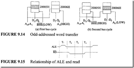
Next, consider writing an odd-addressed 16-bit word by the 8086 using MOV [ BX J ,ex . For example, suppose the 20-bit physical address computed by the 8086 is 20005H. The 8086 accomplishes this transfer in two bus cycles. In the first bus cycle, the 8086 outputs a HIGH on A0 and a LOW on BHE, and thus enables the odd-addressed bank and disables the even-addressed bank. The 8086 also outputs a LOW on the WR and a HIGH on the M/IO pins. In this bus cycle, the 8086 writes data to odd memory bank via D15-D8 lines; the 8086 writes the contents of CL to address 20005H. In the second
image

imagebus cycle, the 8086 outputs a LOW on A0 and a HIGH on BHE and thus enables the even­ addressed bank and disables the odd-addressed bank. The 8086 also outputs a LOW on the WR and a HIGH on the M/10 pins. The 8086 writes data to even memory bank via D7-D0 lines; the 8086 writes the contents of CH to address 20006H. This odd-addressed word write is shown in Figure 9.14.

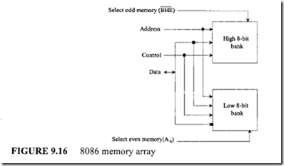
If memory or I/O devices are directly connected to the multiplexed bus, the designer must guarantee that the devices do not corrupt the address on the bus during T1 • To avoid this, the memory or I/O devices should have an output enable controlled by the 8086 read signal. The 8086 timing guarantees that the read is not valid until after the address is latched by ALE as shown in Figure 9.15.

All Intel peripherals, EPROMs, and RAMs for microprocessors provide output enable for read inputs to allow connection to the multiplexed bus. Several techniques are available for interfacing the devices without output enables to the 8086 multiplexed bus. However, these techniques will not be discussed here.


Interfacing with Memories , ROMs and EPROMs , Static RAMs (SRAMs) and Dynamic RAMs (DRAMs)

9.9.3 Interfacing with Memories

In Figure 9.16, the 16-bit word memory in the 8086 is partitioned into odd and even 8- bit banks on the upper and lower halves of the data bus selected by BHE and A0• This is typically used for RAMs. Note that RAMs are needed when subroutines and interrupts requiring stack are desired in an application.

image

imageROMs and EPROMs

ROMs and EPROMs are the simplest memory chips to interface to the 8086. Because ROMs and EPROMs are read-only devices and the 8086 always reads 16-bit data but discards unwanted bytes (if necessary), A0 and BHE are not required to be part of the chip enable/select decoding (chip enable is similar to chip select decoding except that chip enable also provides whether the chip is in active or standby power mode). The 8086 address lines must be connected to the ROM/EPROM chips starting with A 1 and higher to all the address lines of the ROM/EPROM chips. The 8086 unused address lines can be used as chip enable/select decoding. To interface the ROMs/EPROMs directly to the 8086 multiplexed bus, they must have output enable signals. Figure 9.17 shows the 8086 interfaced to two 2732 chips along with the pin diagram of 2732.

The 8086’s interface to 2732 EPROMs in Figure 9.17(b) does not use 8086 BHE and A0 to distinguish between even and odd 2732s. The 8086 RD and inverted M/10 pins are ORed and connected to the 2732 OE pins. The 8086 CE can be connected to either ground or an unused 8086 address pin. Note that both 2732’s are enabled for all data reads; the odd 2732 places data on the demultiplexed 8086 D8-D15 pins while the even 2732 places data on the demultiplexed 8086 D0-D7 pins. The 8086 reads the desired data and discards unwanted data if necessary depending on byte, odd word address or even word address transfers.

image

Static RAMs (SRAMs)

Because static RAMs are read/write memories and data will be written to RAM(s) once selected by the 8086, both A0 and BHE must be included in the chip select logic. For each static RAM, the data lines must be connected to either the upper half (AD15-AD8) or the lower half (AD7-AD0) of the 8086 data lines. Figure 9.18 shows the 8086 interface to two 6116 static RAMs along with the pin diagram of the 6116. Note that the 6116 signals, W (Write Enable), G (Output enable), and E (Chip enable) are decoded as follows: when G = 0 and E = 0, then W = I for read and W = 0 for write.

In Figure 9.18, the 8086 demultiplexed BHE signal is used to select odd 6116 SRAM chips; the data lines of this odd 6116 are connected to the demultiplexed 8086 D8-D15 pins. The 8086 demultiplexed A0 signal, on the other hand, is used to select even 6116 SRAM chip; the data lines of this even 6116 are connected to the demultiplexed 8086

D0-D7 pins. Note that the 6116 has two chip enables E and G along with a single read/write pin (W) .When the 6116 is enabled, W = 1 for read and G = 0 for write.

Dynamic RAMs (DRAMs)

clip_image016Dynamic RAMs store information as charges in capacitors. Because capacitors can hold charges for a few milliseconds, refresh circuitry is necessary in dynamic RAMs for retaining these charges. Therefore, dynamic RAMs are complex devices to use to design a system. To relieve the designer of most of these complicated interfacing tasks, Intel provides dynamic RAM controllers to interface with the 8086 to build a dynamic memory system. Dynamic RAMs are used for microcomputers requiring large memories. DRAMs are typically used when memory requirements are 16k words or larger. DRAM is addressed via row and column addressing. For example, one megabit DRAM requiring 20 address bits is addressed using 10 address lines and two control lines, RAS (Row Address Strobe) and CAS (Column Address Strobe). To provide a 20-bit address into the DRAM, a LOW is applied to RAS and 10 bits of the address are latched. The other 10 bits of the address are applied next and CAS is then held LOW.

The addressing capability of the DRAM can be increased by a factor of 4 by adding one more bit to the address line. This is because one additional address bit results into one additional row bit and one additional column bit. This is why DRAMs can be expanded to larger memory very rapidly with inclusion of additional address bits. External logic is required to generate the RAS and CAS signals, and to output the current address bits to the DRAM.

DRAM controller chips take care of refreshing and timing requirements needed by the DRAMs. DRAMs typically require 4 millisecond refresh time. The DRAM controller performs its task independent of the microprocessor. The DRAM controller sends a wait signal to the microprocessor if the microprocessor tries to access memory during a refresh cycle.

Because oflarge memory, the address lines should be buffered using 74LS244 or 74HC244 (Unidirectional buffer), and data lines should be buffered using 74LS245 or 74HC245 (Bidirectional buffer) to increase the drive capability. Also, typical multiplexers such as 74LS157 or 74HC157 can be used to multiplex the microprocessors address lines into separate row and column addresses.


INTEL 8086 Programming examples Part 1

Example 9.1

(a) Determine the effect of each of the following 8086 instructions:

i). DIV CH            i). CBW            iii). MOVSW Assume the following data prior to execution of each of these instructions independently (assume that all numbers are in hexadecimal): (DS) = 2000H, (ES) = 4000H, (CX) = 0300H, (AX)= 0091H, (20300H) = 05H, (20301H) = 02H, (40200H) = 06H, (40201H) = 07H, (SI) = 0300H, (DI) = 0200H, DF=0.

(b) Write an 8086 assembly language program for each of the following C language program structures:

imageSolution

(a)

i). Before unsigned division, CH contains 0310 and AX contains 14510• Therefore, after DIV CH, (AH) =remainder= OIH and (AL) =quotient= 48 10 = 30H.

ii). CBW sign-extends the AL register into the AH register. Because the content of AL is 91H, the sign bit is 1. Therefore, after CBW, (AX)= FF91H

image

(b)

i). Assume addresses x and y are initialized with the contents of the 8086 memory locations addressed by offsets BX and SI in segment register, DS:

image

Example 9.2

(a) Write an 8086 assembly program to find (X2)/255 where X is an 8-bit signed number stored in CH. Store the 16-bit result onto the stack. Initialize SS and SP to 1000H and 2000H respectively.

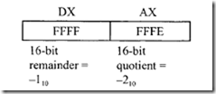
(b) What are the remainder, quotient, and registers containing them after execution of the following 8086 instruction sequence?

image

imageExample 9.3

Write an 8086 assembly language program to add two 16-bit numbers in CX and DX and store the result in location 0500H addressed by DI.

Solution

imageExample 9.4

Write an 8086 assembly language program to add two 64-bit numbers. Assume SI and DI contain the starting offsets of the numbers. Store the result in memory pointed to by DI. Solution

image

imageExample 9.5

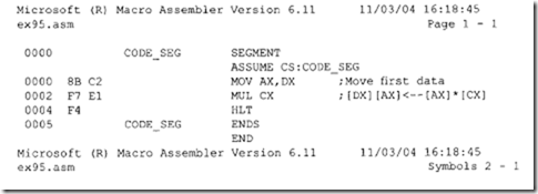
Write an 8086 assembly language program to multiply two 16-bit unsigned numbers to provide a 32-bit result. Assume that the two numbers are stored in CX and DX.

Solution

image

imageExamule 9.6

Write an 8086 assembly language program to clear 5010 consecutive bytes starting at offset 1000H. Assume DS is already initialized.

Solution

imageExamule 9.7

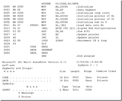
Write an 8086 assembly program to implement the following C language program loop: sum= 0;

for (i = 0; i <=99; i = i + 1)

sum= sum+ x[i] * y[i];

The assembly language program will compute LxJ’; where X; andY; are signed 8-bit numbers stored at offsets 4000H and 5000H respectively. Initialize DS to 2000H. Store 16-bit result in DX. Assume no overflow.

Solution

image

imageExample 9.8

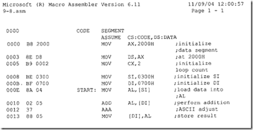
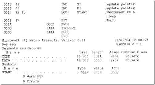
Write an 8086 assembly language program to add two words; each contains two ASCII digits. The first word is stored in two consecutive locations with the low byte pointed to by SI at offset 0300H, while the second word is stored in two consecutive locations with the low byte pointed to by DI at offset 0700H. Store the unpacked BCD result in memory location pointed to by DI. Assume that each unpacked BCD result of addition is less than or equal to 09H.

Solution

image

image

Example 9.9

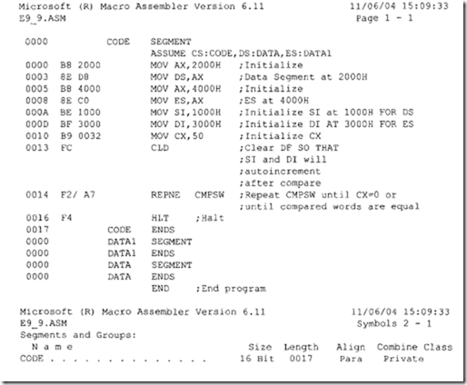
Write an 8086 assembly language program to compare a source string of 5010 words pointed to by an offset 1 OOOH in the data segment at 2000H with a destination string pointed to by an offset 3000H in the extra segment at 4000H. The program should be halted as soon as a match is found or the end of the string is reached.

Solution

image

image

Example 9.10

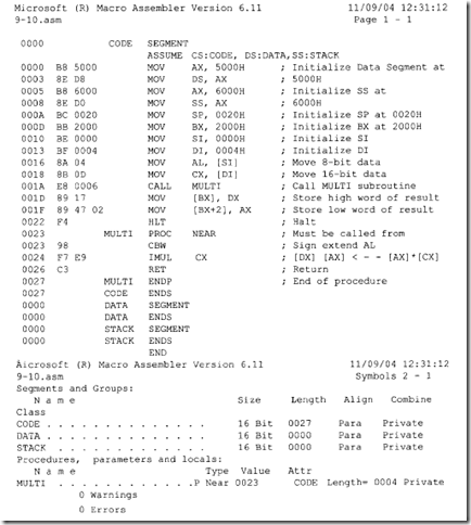
Write a subroutine in 8086 assembly language which can be called by a main program in the same code segment. The subroutine will multiply a signed 16-bit number in CX by a signed 8-bit number in AL. The main program will perform initializations (DS to 5000H, SS to 6000H, SP to 0020H and BX to 2000H), call this subroutine, store the result in two consecutive memory words, and stop. Assume SI and DI contain pointers to the signed 8-bit and 16-bit data respectively. Store 32-bit result in a memory location pointed to by BX.

Solution

image


INTEL 8086 Programming examples Part 2

Example 9.11

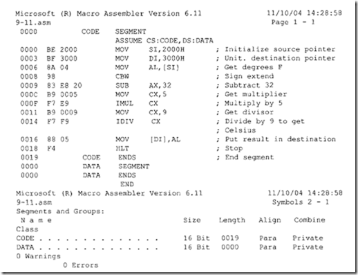
Write an 8086 assembly program that converts a temperature (signed) from Fahrenheit degrees stored at an offset contained in SI to Celsius degrees. The program stores the 8-bit integer part of the result at an offset contained in DI. Assume that the temperature can be represented by one byte and, DS is already initialized. The source byte is assumed to reside at offset 2000H in the data segment, and the destination byte at an offset of 3000H in the same data segment. Use the formula: C = (F-32)/9 x 5

Solution

image

Example 9.12

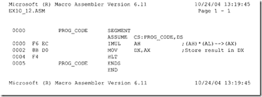
Write an 8086 assembly language program to multiply two 8 bit signed numbers stored in the same register; AH holds one number and AL holds the other number. Store the 16- bit result in DX.

Solution

image

image

Example 9.13

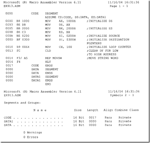
Write an 8086 assembly language program to move a block of 16-bit data oflength 10010 from the source block starting at offset 0200H to the destination block starting at offset 0300H from low to high addresses.

Solution

imageExample 9.14

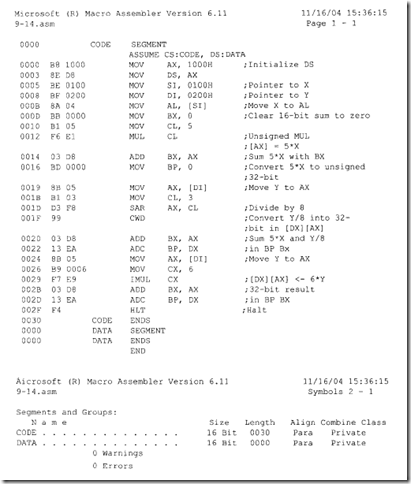
Write an 8086 assembly language program that will perform: 5 x X+ 6 x Y + (Y/8) (BP)(BX) where X is an unsigned 8-bit number stored at offset 01 OOH and Y is a 16-bit signed number stored at offsets 0200H and 0201H. Neglect the remainder of Y/8. Store the result in registers BX and BP. BX holds the low 16-bit of the 32-bit result and BP holds the high 16-bit of the 32-bit result.

Solution

imageExample 9.15

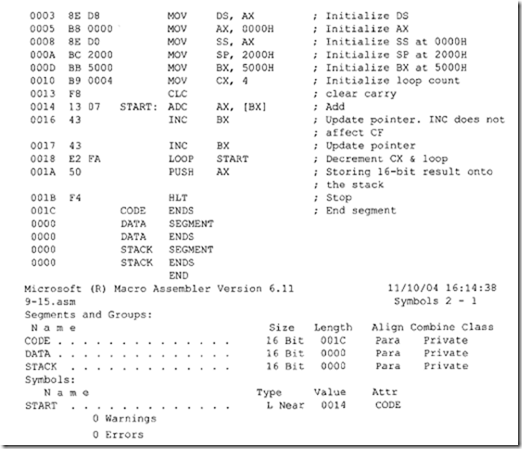
Write an 8086 assembly language program to add four 16-bit numbers stored in consecutive locations starting at offset 5000H. Store the 16-bit result onto the stack. Use ADC instruction for addition.

Solution

image

image

Example 9.16

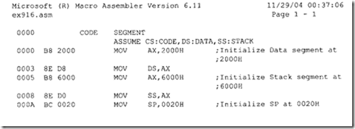
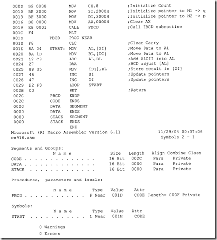
Write a subroutine in 8086 assembly language in the same code segment as the main program to implement the C language assignment statement: p = p + q; where addresses p and q hold two 16-digit (64-bit) packed BCD numbers (Nl and N2). The main program will initialize addresses p and q to DS:2000H and DS:3000H respectively. Address DS:2007H will hold the lowest byte ofNl with the highest byte at address DS:2000H while address DS:3007H will hold the lowest byte of N2 with the highest byte at address DS:3000H. Also, write the main program at offset 7000H which will perform all initializations including DS to 2000H, SS to 6000H, SP to 0020H, SI to 2000H, DI to 3000H, loop count to 8 and, then call the subroutine.

Solution

image

image

Example 9.17

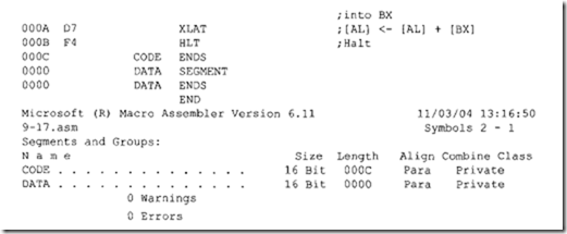
Write an 8086 assembly language program to move the 8-bit contents of a memory location addressed by the contents of AL and BX into AL. Use XLAT instruction. This program will illustrate that XLAT is equivalent to MOV AL, [AL][BX].

Solution

image

imageExample 9.18

Write a subroutine in 8086 assembly language which can be called by a main program in a different code segment. The subroutine will compute IX/ IN. Assume the X/s are 16-bit signed integers, N = 100 and, IX/ is 32-bit wide. The numbers are stored in consecutive locations. Assume SI points to the X/s. The subroutine will start at an offset 7000H, and will initialize SI to 4000H, compute IX/ IN, and store 32-bit result in DX:AX (16-bit remainder in DX and 16-bit quotient in AX). Also, write the main program which will initialize DS to 2000H, SS to 6000H, SP to 0040H, call the subroutine, and stop.

Solution

image

image

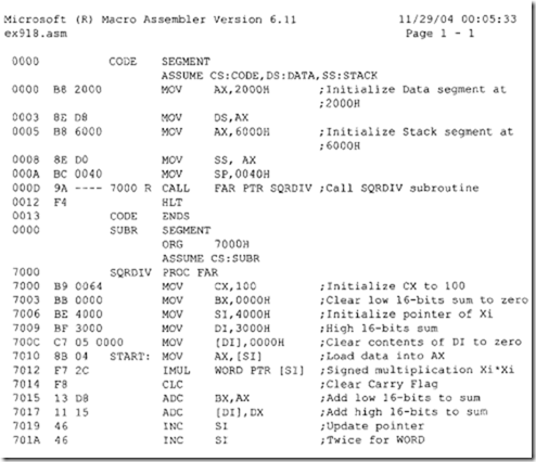
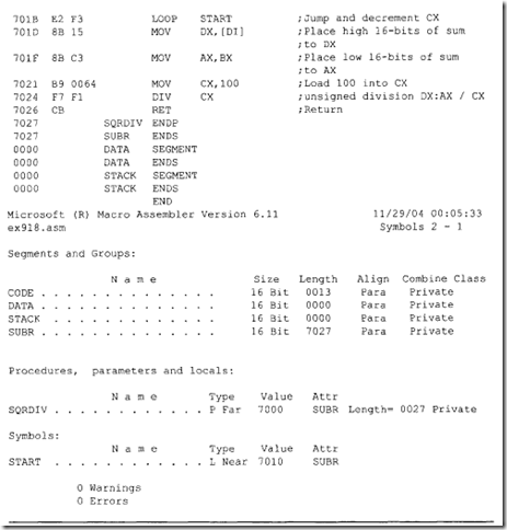
Note: In the above, DIY is used for computing sum (Xi**2)/N since both SUM (Xi**2) and N are unsigned (positive). Also, in order to execute the above program, values for Xi must be stored in memory using 8086 assembler directive, DW.


Processor Control Instructions , 8086 Assembler-Dependent Instructions , Typical8086 Assembler Pseudo-Instructions or Directives , SEGMENT and ENDS Directives , ASSUME Directive , DUP, LABEL, and Other Directives , 8086 Stack and 8086 Delay routine

9.5.8 Processor Control Instructions

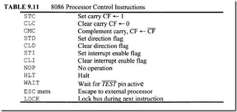
Table 9.11 shows the processor control functions. Let us explain some of the instructions in Table 9.11.

  • ESC mem places the contents of the specified memory location on the data bus at the time when the 8086 ready pin is asserted by the addressed memory device. This instruction is used to pass instructions to a coprocessor such as the 8087 math coprocessor which shares the address and data bus with the 8086.
  • LOCK prefix allows the 8086 to ensure that another processor does not take control of the system bus while it is executing an instruction which uses the system bus. LOCK prefix is placed in front of an instruction so that when the instruction with the LOCK prefix is executed, the 8086 outputs a LOW on the LOCK pin of the 8086 for the duration of the next instruction. This Lock signal is connected to an external bus controller which prevents any other processor from taking over the system bus. Thus the LOCK prefix is used in multiprocessing.
  • WAIT causes the 8086 to enter an idle state if the signal on the TEST input pin is not asserted. This means that the 8086 will remain in the idle state until its TEST pin is asserted. The WAIT instruction can be used to synchronize the 8086 with other external hardware such as the 8087 (Math coprocessor).

9.6 8086 Assembler-Dependent Instructions

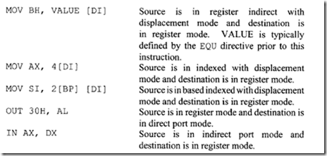
Some 8086 instructions do not define whether an 8-bit or a 16-bit operation is to be executed. Instructions with one of the 8086 registers as an operand typically define the operation as 8-bit or 16-bit based on the register size. An example is MOV CL, [ BX] , which moves an 8-bit number with the offset defined by [BX] in DS into register CL; MOV ex, [BX] , on the other hand, moves a 16-bit number from offsets (BX) and (BX + 1) in DS into CX Instructions with a single-memory operand may define an 8-bit or a 16-bit operation by adding B for byte or W for word with the mnemonic. Typical examples are

image

MULB [BX] and IDIVW [ADDR]. The string instructions may define this in two ways. Typical examples are MOVSB or MOVS BYTE for 8-bit and MOVSW or MOVS WORD for 16-bit. Memory offsets can also be specified by including BYTE PTR for 8-bit and WORD PTR for 16-bit with the instruction. Typical examples are INC BYTE PTR [ BX] and INC WORD PTR [BX].

9.7 Typical8086 Assembler Pseudo-Instructions or Directives

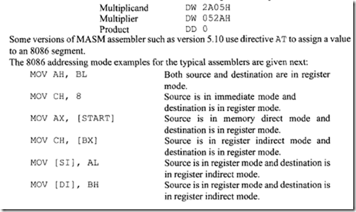
One of the requirements oftypical8086 assemblers such as MASM (discussed later) is that a variable’s type must be declared as a byte (8-bit), word (16-bit), or double word (4 bytes or 2 words) before using the variable in a program. Some examples are as follows:

image

Note that the directive DD is not used by all assemblers. In that case, one should use the directive DW twice to declare a 32-bit offset.

The EQU directive can be used to assign a name to constants. For example, the statement NUMB EQU 21H directs the assembler to assign the value 21H every time it finds NUMB in the program. This means that the assembler reads the statement MOV BH, NUMB as MOV BH, 21H. As mentioned before, DB, DW, and DD are the directives used to assign names and specific data types for variables in a program. For example, after execution of the statement ADDR ow 2050H the assembler assigns SOH to the offset name ADDR and 20H to the offset name ADDR + 1. This means that the program can use the instruction MOV BX, [ADDR] to load the 16-bit contents of memory starting at the offset ADDR in DS into BX. The DW sets aside storage for a word in memory and gives the starting address of this word the name ADDR.

image

imageIn the following paragraphs, more assembler directives such as SEGMENT, ENDS, ASSUME, and DUP will be discussed.

9.7.1 SEGMENT and ENDS Directives

A section of a an 8086 program or a data array can be defined by the SEGMENT and ENDS directives as follows:

imageThe segment name is START (arbitrarily chosen). The assembler will assign a numeric value to START corresponding to the base value of the data segment. The programmer must use the 8086 instructions to load START into DS as follows:

imageNote that all segment registers except CS must be loaded via a 16-bit general purpose register such as BX. A data array or an instruction sequence between the SEGMENT and ENDS directives is called a logical segment. These two directives are used to set up a logical segment with a specific name. A typical assembler allows one to use up to 31 characters for the name without any spaces. An underscore is sometimes used to separate words in a name, for example, PROGRAM_ BEGIN.

9.7.2 ASSUME Directive

As mentioned before, at any time the 8086 can directly address four physical segments, which include a code segment, a data segment, a stack segment, and an extra segment. The 8086 may contain a number of logical segments containing codes, data, and stack. The ASSUME directive assigns a logical segment to a physical segment at any given time. That is, the ASSUME directive tells the assembler what addresses will be in the segment registers at execution time.

For example, the statement ASSUME CS: PROGRAM_1, OS: DATA_1, SS: STACK_1 directs the assembler to use the logical code segment PROGRAM _I as CS, containing the instructions, the logical data segment OATA_I as OS, containing data, and the logical stack segment STACK _I as SS, containing the stack.

9.7.3 DUP, LABEL, and Other Directives

The DUP directive can be used to initialize several locations to zero. For example, the statement START DW 4 DUP ( 0) reserves four words starting at the offset START in DS and initializes them to zero. The DUP directive can also be used to reserve several locations that need not be initialized. A question mark must be used with DUP in this case. For example, the statement BEGIN DB 100 DUP (?) reserves 100 bytes of uninitialized data space to an offset BEGIN in DS. Note that BEG IN should be typed in the label field, DB in the OP code field, and 10 0 DUP (?) in the operand field.

A typical example illustrating the use of these directives is given next:

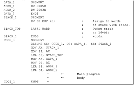
imageNote that LABEL is a directive used to the allocate stack from the next location after the top of the stack. The statement STACK_ TOP LABEL WORD allocates the stack for local variables from the next address after STACK_ TOP. In this example, 60 words are set aside for the stack. The WORD in this statement indicates that PUSH into and POP from the stack are done as words.

Also note that in the above, ASSUME directive tells the assembler to use the logical segment names CODE_I, DATA_I, and STACK_I as the code segment, data segment, and stack segment, respectively. The extra segment can be assigned a name in a similar manner. When the instructions are executed, the displacements in the instructions along with the segment register contents are used by the assembler to generate the 20-bit physical addresses. The segment register, other than the code segment, must be initialized before it is used to access data. The code segment is typically initialized upon hardware reset or by using ORG.

When the assembler translates an assembly language program, it computes the displacement, or offset, of each instruction code byte from the start of a logical segment that contains it. For example, in the preceding program, the CS: CODE_l in the ASSUME statement directs the assembler to compute the offsets or displacements by the following instructions from the start of the logical segment CODE_ I. This means that when the program is run, the CS will contain the 16-bit value where the logical segment CODE_ I is located in memory. The assembler keeps track of the instruction byte displacements, which are loaded into IP. The 20-bit physical address generated from CS and IP are used to fetch each instruction. Some versions of MASM use directive AT to assign a segment value.

Note that typical 8086 assemblers such as Microsoft and Hewlett-Packard HP64000 use the ORG directive to load CS and IP. For example, CS and IP can be initialized with 2000H and 0300H as follows:

image9.7.4 8086 Stack

Each 8086 stack segment is 64K bytes long and is organized as 32K 16-bit words. The lowest byte (valid data) of the stack is pointed to by the 20-bit physical address computed from current SP and SS. This is the lowest memory location in the stack (Top of the Stack) where data is pushed. The 8086 PUSH and POP instructions always utilize 16-bit words. Therefore, stack locations should be configured at even addrsesses in order to minimize the number of memory cycles for efficient stack operations. The 8086 can have several stack segments; however, only one stack segment is active at a time.

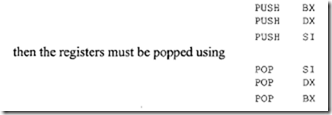
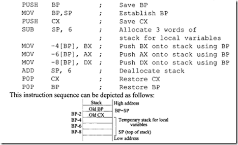
Since the 8086 uses 16-bit data for PUSH and POP operations from the top of the stack, the 8086 PUSH instruction first decrements SP by 2 and then the 16-bit data is written onto the stack. Therefore, the 8086 stack grows from high to low memory addresses of the stack. On the other hand, when a 16-bit data is popped from the top of the stack using the 8086 POP instruction , the 8086 reads 16-bit data from the stack into the specified register or memory, the 8086 then increments the SP by 2. Note that the 20-bit physical address computed from SP and SS always points to the last data pushed onto the stack. One can save and restore flags in the 8086 using PUSHF and POPF instructions. Memory locations can also be saved and restored using PUSH and POP instructions without using any 8086 registers. Finally, One must POP registers in the reverse order in which they are PUSHed. For example, if the registers BX, DX, and SI are PUSHed using

image9.8 8086 Delay routine

Typical 8086 software delay loops can be written using MOV and LOOP instructions. For example, the following instruction sequence can be used for a delay loop of 20 millisecond:

imageautodecrementing CX by 1. However, the 8086 goes to the next instruction and does not branch when CX = 0 after autodecrementing CX by 1, and this requires 5 cycles. This means that the DELAY loop will require 17 cycles for (count – 1) times, and the last iteration will take 5 cycles.

For 2-MHz 8086 clock, each cycle . 500ns. For 20 ms, total cycles=image 40,000. The loop will require 17 cycles for (count – 1) times when CX 1= 0 and 5 cycles will be required when no branch is taken (CX = 0). Thus, totai cycles including the MOV = 4+ 17x(count – 1) + 5= 40,000. Hence, count e 2353 10 = 0931 16• Therefore, CX must be loaded with 2353 10 or 0931 16 •

Now, in order to obtain delay of 20 seconds, the above DELAY loop of 20  millisecond can be used with an external counter. Counter value= (20 sec) I (20 msec) = 1000. The following instruction sequence will provide an approximate delay of 20 seconds:

image

Next, the delay time provided by the above instruction sequence can be calculated. From Appendix F, the cycles required to execute the following 8086 instructions:

imageAs before, assuming 4-MHz 8086 clock, each cycle is 250ns. Total time from the above instruction sequence for 20-second delay = Execution time for MOV DX + 1000 * (20 msec delay)+ 1000 *(Execution time for DEC)+ 999* (Execution time for JNE for Z = 0 when DX 1= 0) +(Execution time for JNE for Z = 1 when DX = 0) = 4 * 250ns + 1000 * 20msec + 1000 * 2 * 250ns + 999 * 16 * 250ns + 4 * 250ns e 20.0045 seconds which is approximately 20 seconds discarding the execution times of MOV DX, DEC, and JNE.


Unconditional Transfer Instructions , Conditional Branch Instructions , Iteration Control Instructions and Interrupt Instructions

9.5.1 Unconditional Transfer Instructions

Unconditional transfer instructions transfer control to a location either in the current executing memory segment (intrasegment) or in a different code segment (intersegment). Table 9.5 lists the unconditional transfer instructions.

The 8086 CALL instructions provide the mechanism to call a subroutine into operation while the RET instruction placed at the end of the subroutine transfers control back to the main program. There are two types of 8086 CALL instruction. These are intrasegment CALL (IP changes, CS is fixed), and intersegment CALL (both IP and CS are changed). Intrasegment or Intersegment CALL is defined by the various operands of the CALL instruction. For example, the three operands NEAR PROC, meml6, and regl6 define intrasegment CALLs to a subroutine. Upon execution of the intrasegment CALL with any of the three operands, the 8086 pushes the current contents of IP onto the stack; the SP is then decremented by 2. The saved IP value is the offset that contains the next instruction to be executed in the main program. The 8086 then places a new I 6-bit value ( Offset of the first instruction in the subroutine) into IP. The three types of operands of the intrasegment CALL will be discussed next.

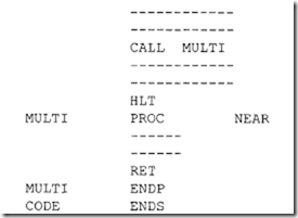
Consider CALL NEAR PROC. The assembler directive NEAR specifies the CALL instruction with relative addressing mode. This means that NEAR determines a I 6- bit displacement, and the offset is computed relative to the address of the CALL instruction. With 16-bit displacement, the range of the CALL instruction is limited to -32766 to+ 32765 (0 being positive). As an example, consider the following 8086 instruction sequence:

image

image

In the above, the main program is located in a segment named CODE. A subroutine called MULTI is also resident in the same code segment named CODE. Since this subroutine is in the same code segment as the main program containing the CALL instruction, the contents of CS are not altered to access it. Use of the assembler directive NEAR in the statement MULTI PROC NEAR tells the 8086 assembler that the main program and the subroutine are located in the same code segment.

The instructions CALL me m 16 and CALL re g 16 specify a memory location or a 16-bit register such as BX to hold the offset to be loaded into IP. Thus, these two CALL instructions use indirect addressing mode. An example of CALL me m 16 is CALL [BX] which loads the 16-bit value stored in the memory location pointed to by BX into IP. The physical address of the offset is calculated from the current DS and the contents of BX. The first instruction of the subroutine is contained in the address computed from new IP value and current CS. Next, typical examples of CALL regl6 are CALL BX and CALL BP; these instructions load the 16-bit contents of BX or BP into IP. The starting address (physical address) of the subroutine is computed from the new value of iP and the current CS contents. Note that intrasegment CALL instructions are used when the main program and the subroutine are located in the same code segment.

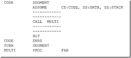
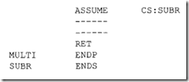
Intersegment CALL instructions are used when the main program and the subroutine are located in two different code segments. The two intersegment CALL instructions are CALL FAR PROC and CALL mem32. These instructions define a new offset for IP and a new value for CS. Upon execution of these two instructions, the 8086 pushes the current contents of IP and CS onto the stack, the new values of IP and CS are then loaded. For example consider CALL FAR PROC which loads the new value of IP from the next two bytes, and the new value of CS from the following two bytes. As an example, consider the following 8086 instruction sequence:

image

image

In the above, the main program is located in a segment named CODE. A subroutine called MULTI is in a segment named SUBR. Since this subroutine is in a different code segment from the CALL instruction, the contents of CS must be altered to access it. Use of the assembler directive FAR in the statement MULTI PROC FAR tells the 8086 assembler that the main program and the subroutine are located in different code segments. When the assembler translates the CALL instruction, it will assign the value of SUBR to CS, and will place the offset of the first instruction of the subroutine in SUBR as the IP value in the instruction.

CALL FAR [SI] stores the pointer for the subroutine as four bytes in data memory. The location of the first byte of the four-byte pointer is specified indirectly by one of the 8086 registers (SI in this case). In this example, the 20-bit physical address of the first byte of the four-byte pointer is computed from DS and Sl. Finally, CALL FAR [BX] pushes CS and IP onto stack and loads IP and CS with the contents of four consecutive bytes pointed to by BX.

RET instruction is usually placed at the end of a subroutine which pops IP (pushed onto the stack by the intrasegment CALL instruction) or both IP and CS (pushed onto the stack by the intersegment CALL instruction), and returns control to the main program. RET disp 16, on the other hand, adds 16-bit value ( disp 16) to SP after placing the return address into IP (for intrasegment CALL) or into IP and CS ((for intersegment CALL). The main objective of inclusion of the 16-bit displacement operand with the RET instruction is to discard the parameters that were saved onto the stack before execution of the subroutine CALL instruction.

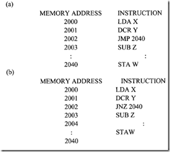
Similar to the CALL instruction, the jump instruction in Table 9.5 can be either intrasegment JMP (Jump within the current code segment; only IP changes) or intersegment JMP (Jump from one code segment to another code segment; both CS and IP contents are modified). Intrasegment Jump can have an operand with a short label, near label, reg16 or meml6. For example, the short label and near label operands use relative addressing mode. This means that the Jump is performed relative to the address of the JMP instruction. For jumps with short label, IP changes and CS is fixed. JMP di sp8 adds the second object code byte (signed 8-bit displacement) to (IP + 2), and (CS) is unchanged. With an 8-bit signed displacement, jump with a short label operand is allowed in the range from -128 to + 127 (0 being positive) from the address of the JMP instruction. Near label operand allows a JMP instruction to have a signed 16-bit displacement with a range -32K to +32K bytes from the address of the JMP instruction. An example of JMP short label or near label is JMP START. The 8086 assembler automatically computes the value of the displacement START at assembly time. The programmer does not have to worry about it. Based upon the displacement size of START (in this case), the assembler determines whether the JMP is to be performed with short or near label.

JMP reg 16 or JMP mem 16 specifies the JUMP address respectively by the I 6- bit contents of of a register or a memory location. The range for this JMP is from -32K to +32K bytes from the address ofthe JMP. An example of JMP reg16 is JMP SI which copies the contents of SI into IP. SI contains the 16-bit displacement. The 8086 computes the physical address from the current CS value and the new IP value. An example of JMP mem16 is JMP [DI] which uses the contents of DI as the address of the memory location containing the offset. This offset is placed into IP. The physical address is computed from this IP value and the current code segment value.

The intersegment JMP instruction includes operands with far label and mem32.

Jump with far label uses a 32-bit immediate operand ; the first 16 bits are loaded into IP while the next 16 bits are loaded into CS. An example of JMP with far label is JMP FAR BEGIN (or some 8086 assemblers use JMP FAR PTR BEGIN) which unconditionally branches to a label BEGIN in a different code segment.

Finally, JMP mem32 indirectly specifies the offset and the code segment values.

IP and CS are loaded from the 32-bit contents of four consecutive memory locations; each memory location contains a byte. As an example, JMP FAR [ S I] loads IP and CS with the contents of four consecutive bytes pointed to by SI in DS.

9.5.2 Conditional Branch Instructions

All 8086 conditional branch instructions use 8-bit signed displacement. That is, the displacement covers a branch range of -128 to +127, with 0 being positive. The structure of a typical conditional branch instruction is as follows:

If condition is true,

then IP +- IP + disp8,

otherwise IP +- IP + 2 and execute next instruction.

There are two types of conditional branch instructions. In one type, the various relationships that exist between two numbers such as equal, above, below, less than, or greater than can be determined by the appropriate conditional branch instruction after a COMPARE instruction. These instructions can be used for both signed and unsigned numbers. When comparing signed numbers, terms such as "less than" and "greater than" are used. On the other hand, when comparing unsigned numbers, terms such as "below zero" or "above zero" are used.

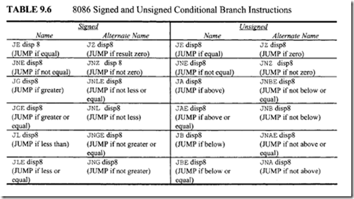
Table 9.6 lists the 8086 signed and unsigned conditional branch instructions. Note that in Table 9.6 the instructions for checking which two numbers are "equal" or

image

image

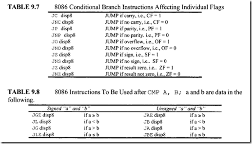
"not equal" are the same for both signed and unsigned numbers. This is because when two numbers are compared for equality, irrespective of whether they are signed or unsigned, they will provide a zero result (ZF = I) if they are equal and a nonzero result (ZF = 0) if they are not equal. Therefore, the same instructions apply for both signed and unsigned numbers for "equal to" or "not equal to" conditions. The second type of conditional branch instructions is concerned with the setting of flags rather than the relationship between two numbers. Table 9.7 lists these instructions.

Now, in order to check whether the result of an arithmetic or logic operation is zero, nonzero, positive or negative, did or did not produce a carry, did or did not produce parity, or did or did not cause overflow, the following instructions should be used: JZ, JNZ, JS, JNS, JC, JNC, JP, JNP, JO, JNO. However, in order to compare two signed or unsigned numbers (a in address A orb in address B) for various conditions, we use CMP A, B, which will form a- b. and then one of the instructions in Table 9.8.

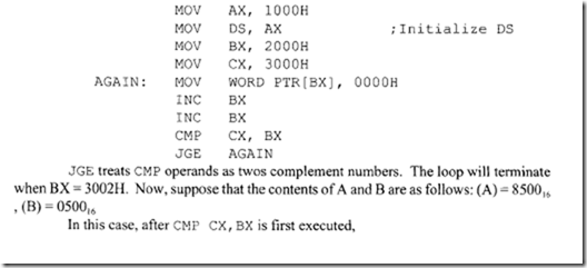
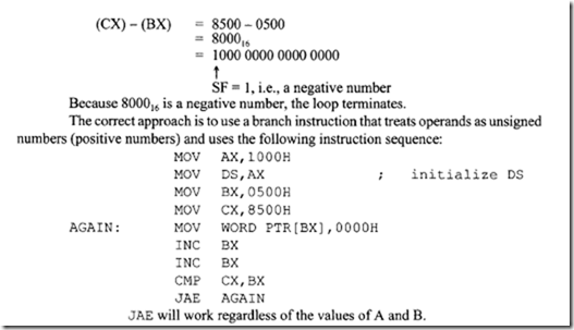
Now let us illustrate the concept of using the preceding signed or unsigned instructions by an example. Consider clearing a section of memory word starting at B up to and including A, where (A)= 3000 16 and (B)= 2000 16 in DS = 100016, using the following instruction sequence:

image

image

Also, note that addresses are always positive numbers (unsigned). Hence, unsigned conditional jump instruction must be used to obtain the correct answer. The above examples are shown for illustrative purposes.

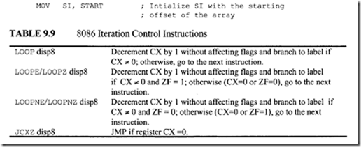
9.5.7 Iteration Control Instructions

Table 9.9 lists iteration control instructions. All these instructions have relative addressing modes.

LOOP disp8 decrements the CX register by 1 without affecting the flags and then acts in the same way as the JMP dsp8 instruction except that if CX ;o< 0, then the JMP is performed: otherwise, the next instruction is executed.

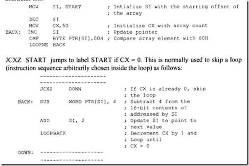
LOOPE (Loop while equal) I LOOPZ (Loop while zero), on the other hand, decrements CX by 1 without affecting the flags. The contents of CX are then checked for zero, and also the zero flag (ZF), that results from execution of previous instruction, is checked for one. If CX ;o! 0 and ZF = 1, the loop continues. If either CX = 0 or ZF = 0, the next instruction after the LOOPE or LOOPZ is executed. The following 8086 instruction sequence compares an array of 50 bytes with data byte OOH. As soon as a match is not found or end of array is reached, the loop exits. LOOPE instruction can be used for this purpose. The following 8086 instruction sequence illustrates this:

image

image

LOOPNE (LOOP while not equal) I LOOPNZ (Loop while not zero) is similar to LOOPE I LOOPZ except that the loop continues if ex ;o0 0 and ZF = 0. On the other hand, If ex = 0 or ZF = 1, the next instruction is executed. The following 8086 instruction sequence compares an array of 50 bytes with data byte 00H for a match. As soon as a match is found or end of array is reached, the loop exits. LOOPNE instruction can be used for this purpose. CX=0 and ZF=0 upon execution of the CMP instruction 50 times in the following would imply that data byte 00H was not found in the array. The following 8086 instruction illustrates this:

image

9.5.8 Interrupt Instructions

Table 9.10 shows the interrupt instructions. INT n is a software interrupt instruction. Execution of INT n causes the 8086 to push current es, IP, and Flags onto the stack, and loads CS and IP with new values based on interrupt type n; an interrupt service routine is written at this new address. IRET at the end of the service routine transfers control to the main program by popping old es, IP, and flags from the stack.

The interrupt on overflow is a type 4 (n = 4) interrupt. This interrupt occurs if the overflow flag (OF) is set and the INTO instruction is executed. The overflow flag

imageis affected, for example, after execution of a signed arithmetic (such as IMUL, signed multiplication) instruction. The user can execute an INTO instruction after the IMUL. If there is an overflow, an error service routine written by the user at the type 4 interrupt address vector is executed.
Interrupt instructions are discussed in detail later in this Chapter.


Intel 8086 : 8086 Instruction Set , Data Transfer Instructions , Arithmetic Instructions , Bit Manipulation Instructions and String Instructions

9.5 8086 Instruction Set

The 8086 has approximately 117 different instructions with about 300 op-codes. The 8086 instruction set contains no-operand, single-operand, and two-operand instructions. Except for string instructions that involve array operations, 8086 instructions do not permit memory-to-memory operations. Appendices F and H provide 8086 instruction reference data and the instruction set (alphabetical order), respectively. The 8086 instructions can be classified into eight groups:

1. Data Transfer Instructions

2. Arithmetic Instructions

3. Bit Manipulation Instructions

4. String Instructions

5. Unconditional Transfer Instructions

6. Conditional Branch Instructions

7. Interrupt Instructions

8. Processor Control Instructions

Let us now explain some of the 8086 instructions with numerical examples. Note that

image

in the following examples , symbol ( ) is used to indicate the contents of a register or a memory location.

9.5.1 Data Transfer Instructions

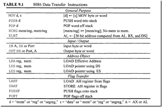
Table 9.1 lists the data transfer instructions. Note that LEA is used to load 16-bit offset to a specified register; LDS and LES are similar to LEA except that they load specified register as well as DS or ES. As an example, LEA BX, 3000H has the same meaning as MOV BX,3000H. On the other hand, if (SI)=2000H, then LEA BX,4[Sl] will load 2004H into BX while MOV BX,4[SI] will initialize BX with the contents of memory locations computed from 2004H and DS. The LEA instruction can be useful when memory computation is desirable.

In Table 9.1, there are 14 data transfer instructions. These instructions move single bytes and words between a register, a memory location, or an I/0 port. Let us explain some of the instructions in Table 9.1.

  • MOV CX, DX copies the 16-bit contents ofDX into ex. MOV AX, 2025H moves immediate data 2025H into the 16-bit register AX. MOV eH, [ BX] moves the 8-bit contents of a memory location addressed by BX in segment register DS into eH. If (BX) = 0050H, (DS) = 2000H, and (20050H) = 08H, then, after MOV eH, [ BX], the contents ofeH will be 08H. MOV START [BP], ex moves the 16-bit (eL to first location and then eH) contents of ex into two memory locations addressed by the sum of the displacement START and BP in segment register SS. For example, if (eX) = 5009H, (BP)=0030H, (SS) = 3000H, and START= 06H, then, after MOV START [ BP l , ex, (30036H) = 09H and (30037H) =SOH.

LDS s I, [ 0 01OH] loads SI and DS from memory. For example, if (DS) = 2000H, (20010) = 0200H, and (20012) = 0100H, then, after LOS SI, [0010], Sl and DS will contain 0200H and 0100H, respectively.

In the 8086, the SP is decremented by 2 for PUSH and incremented by 2 for POP. For example, consider PUSH [BX]. If (DS) = 2000 16, (BX) = 020016, (SP) = 300016, (SS) = 4000 16, and (20200) = 012016, then, after execution of PUSH [BX], memory locations 42FFF and 42FFE will contain 01 16 and 20 16,respectively, and the contents of SP will be 2FFE 16• XCHG has three variations: XCHG reg, reg and XCHG mem, reg or XCHG reg, mem.

For example, XCHG AX, BX exchanges the contents of 16-bit register BX with the contents of AX. XCHG mem, reg exchanges 8- or 16-bit data in mem with 8-or 16-bit reg.

XLAT can be used to employ an index in a table or for code conversion. This instruction utilizes BX to hold the starting address of the table in memory consisting of 8-bit data elements. The index in the table is assumed to be in the AL register. For example, if (BX) = 0200 16, (AL) = 0416, and (DS) = 300016, then, after XLAT, the contents of location 30204 16 will be loaded into AL. Note that the XLAT instruction is the same as MOV AL, [AL] [ BX] . As mentioned before, XLAT instruction can be used to convert from one code to another. For example, consider an 8086-based microcomputer with an ASCII keyboard connected to Port A and an EBCDIC printer connected to Port B. Suppose that it is desired to enter numerical data via the ASCII keyboard, and then print them on the EBCDIC printer. Note that numerical data entered into this computer via the keyboard will be in ASCII code. Since the printer only understands EBCDIC code, an ASCII to EBCDIC code conversion program is required. The ASCII codes for numbers 0 through 9 are 30H through 39H while the EBCDIC codes for numbers 0 to 9 are FOH to F9H (Table 2.6). The EBCDIC codes for the numbers 0 to 9 can be stored in a table starting at an offset 2030H , data can be input from the keyboard using IN AL, PORTA, convert this ASCII data to EBCDIC using XLAT instruction, and then output to Port Busing OUT PORTB, AL. The instruction sequence for the code conversion program is provided below:

imageConsider fixed port addressing, in which the 8-bit port address is directly specified as part of the instruction. IN AL, 38H inputs 8-bit data from port 38H into AL. IN AX, 38 H inputs 16-bit data from ports 38H and 39H into AX. OUT 3 8H, AL outputs the contents of ALto port 38H. OUT 3 8H, AX, on the other hand, outputs the 16-bit contents of AX to ports 38H and 39H.
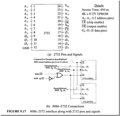
For variable port addressing, the port address is 16-bit and is specified in the DX register. Assume (DX) = 312416 in all the following examples.

IN AL, DX inputs 8-bit data from 8-bit port 312416 into AL.

IN AX, DX inputs 16-bit data from ports 312416 and 312516 into AX.

OUT DX, AL outputs 8-bit data from AL into port 312416• OUT DX, AX outputs 16-bit data from AX into ports 312416 and 3125 16• Variable port addressing allows up to 65,536 ports with addresses from 0000H to FFFFH. The port addresses in variable port addressing can be calculated dynamically in a program. For example, assume that an 8086-based microcomputer is connected to three printers via three separate ports. Now, in order to output to each one of the printers, separate programs are required if fixed port addressing is used. However, with variable port addressing, one can write a general subroutine to output to the printers and then supply the address of the port for a particular printer in which data output is desired to register DX in the subroutine.

9.5.2 Arithmetic Instructions

Table 9.2 shows the 8086 arithmetic instructions. These operations can be performed on four types of numbers: unsigned binary, signed binary, unsigned packed decimal, and signed packed decimal numbers. Binary numbers can be 8 or 16 bits wide. Decimal numbers are stored in bytes; two digits per byte for packed decimal and one digit per byte for unpacked decimal with the high 4 bits filled with zeros.

Let us explain some of the instructions in Table 9.2.

  • Consider ADC mem/reg , mem/reg. This instruction adds source and destination data along with the carry flag, and stores the result in destination. There is no ADC mem , mem instruction. All flags in the low byte of the Flag register are affected. For example, if (AX) = 0020 16, (BX) = 0300 16> CF = I, (DS) = 2020 16, and (20500) = 0 I 0016, then, after ADC AX, [BX] , the contents of register AX = 0020 + 0 I 00 + I = OI21 16; CF = 0, PF = 0 (Result with odd Parity), AF = 0, ZF = 0 (Nonzero Result), SF = 0 (Most Significant bit of the result is zero), and OF = 0.
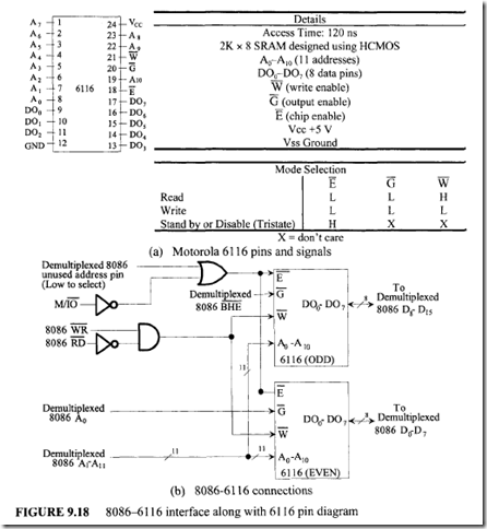
  • Consider SBB mem/reg , mem/reg. This instruction subtracts source data and the carry flag from destination data, and stores the result in destination. There is no SBB mem, mem instruction. All flags in the low byte of the Flag register are affected. For example, if(CH) = 0316, (DL) = 0216, and CF =I, then, after SBB CH,DL, the contents of register CH = 03- 02- I= 0016
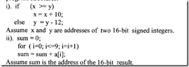
imageFinal carry is one’s complemented after subtraction to reflect the correct borrow. Hence, CF = 0. Also, PF = 1 (Even parity; number of I ‘sin the result is 0 and 0 is an even number), AF =I, ZF = 1 (Zero Result), SF= 0 (Most Significant bit of the result is zero), and OF= cf EB CP =I EB I= 0.

  • The Compare (CMP) instruction subtracts source from destination providing no result of subtraction; all status flags are affected based on the result. Note that the SUBTRACT instruction provides the result and also affects the status flags. Consider CMP DH, BL. If prior to execution of the instruction, (DH) = 40H and (BL) = 30H then after execution of CMP DH, BL, the flags are: CF = 0, PF = 0, AF = 0, ZF = 0, SF = 0, and OF= 0; result 1OH is not provided. Suppose it is desired to find the number of matches for an 8-bit number in an 8086 register such as DL in a data array of 50 bytes in memory pointed to by BX in DS. The following instruction sequence with CMP DL, [ BX] rather than SUB DL, [ BX] can be used :

image

image

In the above, ifSUB DL, [BX) wereused instead of CMP DL, [BX), then the number to be matched needed to be loaded after each subtraction because the contents of DL would have been lost after each SUB. Since we are only interested in the match rather than the result, CMP DL, [BX) instead of SUB DL, [BX) should be used in the above. Numerical data received by an 8086-based microcomputer from a terminal is usually in ASCII code. The ASCII codes for numbers 0 to 9 are 30H through 39H. Two 8-bit data items can be entered into an 8086-based microcomputer via a keyboard. The ASCII codes for these data items (with 3 as the upper nibble for each type) can be added. AAA instruction can then be used to provide the correct unpacked BCD. Suppose that ASCII codes for 2 (3216) and 5 (3516) are entered into an 8086-based microcomputer via a keyboard. These ASCII codes can be added and then the result can be adjusted to provide the correct unpacked BCD using the AAA instruction as follows:

image

Note that, in order to print the unpacked BCD result 0716 on an ASCII printer, (AL) = 07 can be ORed with 30H to provide 37H, the ASCII code for 7.

In case of an invalid BCD digit after addition, AAA instruction can be used to obtain correct unpacked BCD as follows:


image

  • DAA is used to adjust the result of adding two packed BCD numbers in AL to provide a valid BCD number. If, after the addition, the low 4 bits of the result in AL is greater than 9 (or if AF = I), then the DAA adds 6 to the low 4 bits of AL. On the other hand. if the high 4 bits of the result in AL are greater than 9 (or if CF = 1), then DAA adds 60H to AL.
  • DAS may be used to adjust the result of subtraction in AL of two packed BCD numbers to provide the correct packed BCD. While performing these subtractions, any borrows from low and high nibbles are ignored, For example, consider subtracting packed BCD 55 in DL from packed BCD 94 in AL:

image

The invalid BCD digit (F) in the low 4 bits of the result can be corrected by subtracting 6 from F:

image

  • For 8-bit by 8-bit signed or unsigned multiplication between the contents of a memory location and AL, assembler directive BYTE PTR can be used. Example: IMUL BYTE PTR[BX]. On the other hand, for 16-bit by 16-bit signed or unsigned multiplication between the 16-bit contents of a memory location and register AX, assembler directive WORD PTR can be used. Example: MUL WORD PTR[SI].
  • Consider 16 x 16 unsigned multiplication, MUL WORD PTR [BX]. If(BX) = 0050H, (DS) = 3000H, (30050H) = 0002H, and (AX) = 0006H, then, after MUL WORD PTR [BX], (DX) = 0000H and (AX)= 000CH.
  • MUL mem/reg provides unsigned 8 x 8 or unsigned 16 x 16 multiplication. Consider MUL BL. If (AL) = 20 16 and (BL) = 02 16, then, after MUL BL, register AX will contain 004016·
  • IMUL mem/reg provides signed 8 x 8 or signed 16 x 16 multiplication. As an example, if (CL) = FDH = -310 and (AL) = FEH = -210, then, after IMUL CL, register AX contains 0006H.
  • ConsideriMUL DH. If(AL)=FF 16 =-1 10 and(DH)=02 16,then,afteriMUL DH, register AX will contain FFFE 16 (-210) .
  • DIV mem/reg performs unsigned division and divides (AX) or (DX:AX) registers by reg or mem. For example, if(AX) = 0005 16 and (CL) = 0216, then, after DIV CL, (AH) = 01 16 =Remainder and (AL) = 0216 Quotient.
  • Consider DIV BL. If(AX) = 0009H and (BL) = 02H, then, after DIV BL,

(AH) = remainder = 0 I H

(AL) =quotient= 04H

  • IDIV mem/reg performs signed division and divides 16-bit contents of AX by an 8-bit number in a register or a memory location, or 32-bit contents of DX:AX registers by a 16-bit number in a register or a memory location. Consider IDIV CX. If (CX) = 2 and (DXAX) = -510 = FFFFFFFB 16, then, after this IDIV, registers DX and AX will contain:

image

Note that in the 8086, after IDIV, the sign of remainder is always the same as the dividend unless the remainder is equal to zero. Therefore, in this example, because the dividend is negative (-510), the remainder is negative (-1 10).

  • For 16-bit by 8-bit signed or unsigned division of the 16-bit contents of AX by 8-bit contents of a memory location, assembler directive BYTE PTR can be used. Example: IDIV BYTE PTR[BX]. On the other hand, for 32-bit by 16-bit signed or unsigned division of the 32-bit contents of DXAX by 16-bit contents of a memory location, assembler directive WORD PTR can be used. Example: MUL WORD PTR[SI].
  • Consider IDIV WORD PTR [BX]. lf(BX) = 0020H, (DS) = 2000H, (20020H) = 0004H, and (DX) (AX)= 00000011H, then, after IDIV WORD PTR [BX], (DX) =remainder= OOOIH (AX)= quotient= 0004H
  • Consider CBW. This instruction extends the sign from the AL register to the AH register. For example, if AL = Fl 16, then, after execution of CBW, register AH will contain FF16 because the most significant bit ofFl 16 is 1. Note that the sign extension is very useful when one wants to perform an arithmetic operation on two signed numbers of different lengths. For example. the 16-bit signed number 002016 can be added with the 8-bit signed number El 16 by sign-extending El as follows:

image

  • Another example of sign extension is that, to multiply a signed 8-bit number by a signed 16-bit number, one must first sign-extend the signed 8-bit into a signed I6-bit number and then the instruction IMUL can be used for 16 x 16 signed multiplication. For unsigned multiplication of a 16-bit number by an 8-bit number, the 8-bit number must be zero extended to 16 bits using logical instruction such as AND before using the MUL instruction.
  • CWO sign-extends the AX register into the DX register. That is, if the most significant bit of AX is I, then FFFF16 is stored into DX.
  • AAD converts two unpacked BCD digits in AH and ALto an equivalent binary number in AL after converting them to packed BCD. AAD must be used before dividing two unpacked BCD digits in AX by an unpacked BCD byte. For example, consider dividing (AX) =unpacked BCD 0508 (58 Packed BCD) by (DH) = 07H. (AX) must first be converted to binary by using AAD. The register AX will then contain 003AH =58 Packed BCD. After DIV DH, (AL) =quotient= 08 (unpacked BCD), and (AH) =remainder 02 (unpacked BCD).
  • AAM adjusts the product of two unpacked BCD digits in AX. If(AL) = 03H (unpacked BCD for 3) = 0000001I 2 and (CH) = 08H (unpacked BCD for 8) = 0000 10002, then, after MUL CH, {AX) = 00000000000 li 0002 = 00 ISH, and, after using AAM, (AX) = 0000001000000 I 002 = unpacked 0204. The following instruction sequence accomplishes this:

MUL CH

AAM

Note that the 8086 does not allow multiplication of two ASCII codes. Therefore, before multiplying two ASCII bytes received from a terminal, one must make the upper 4 bits of each one of these bytes zero, multiply them as two unpacked BCD digits, and then use AAM for adjustment to convert the unpacked BCD product back to ASCII by ORing the product with 3030H. The result in decimal can then be printed on an ASCII printer.

9.5.3 Bit Manipulation Instructions

The 8086 provides three groups of bit manipulation instructions. These are logicals, shifts, and rotates, as shown in Table 9.3. The operand to be shifted or rotated can be either 8- or 16-bit. Let us explain some of the instructions in Table 9.3

Consider AND BH, 8FH. If prior to execution of this instruction, (BH) = 72H, then after execution of AND BH, 8FH, the following result is obtained:

imageZF = 0 (Result is nonzero), SF = 0 (Most Significant Bit of the result is 0), PF = 0 (Result has odd parity). CF, AF, and OF are always cleared to 0 after logic operation. The status flags are similarly affected after execution of other logic instructions such as OR, XOR, NOT, and TEST.

The AND instruction can be used to perform a masking operation. If the bit value in a particular bit position is desired in a word, the word can be logically ANDed with appropriate data to accomplish this. For example, the bit value at bit 2 of an 8- bit number 0100 1Y10 (where unknown bit value of Y is to be determined) can be obtained as follows:

image

If the bit value Y at bit 2 is 1, then the result is nonzero (Flag Z=O); otherwise, the result is zero (Flag Z= 1) . The Z flag can be tested using typical conditional JUMP instructions such as JZ (Jump if Z= 1) or JNZ (Jump if Z=O) to determine whether Y

TABLE9.3image

is 0 or 1. This is called masking operation. The AND instruction can also be used to determine whether a binary number is ODD or EVEN by checking the Least Significant bit (LSB) of the number (LSB=O for even and LSB=l for odd).

  • Consider OR DL, AH. If prior to execution of this instruction, [DL] = A2H and [AH] = 5DH, then after exection of OR DL, AH, the contents of DL are FFH. The flags are affected similar to the AND instruction. The OR instruction can typically be used to insert a 1 in a particular bit position of a binary number without changing the values of the other bits. For example, a 1 can be inserted using the OR instruction at bit number 3 of the 8-bit binary number 0 I I 1 0 0 1 1 without changing the values of the other bits as follows:
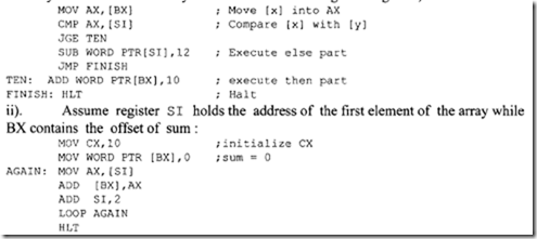
image

  • Consider XOR ex, 2 . If prior to execution of this instruction, (ex) = 2342H, then after execution of XOR ex, 2, the 16-bit contents of CX will be 2340H. All flags are affected in the same manner as the AND instruction. The Exclusive-OR instruction can be used to find the ones complement of a binary number by XORing the number with all 1’s as follows:
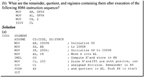
image

  • TEST eL, 05H logically ANDs (CL) with 00000101 2 but does not store the result in CL. All flags are affected.
  • Consider SHR mem/reg, eNT or SHL mem/reg, eNT. These instructions are logical right or left shifts, respectively. The CL register contains the number of shifts if the shift is greater than 1. If eNT = 1, the shift count is immediate data. In both cases, the last bit shifted out goes to CF (carry flag) and 0 is the last bit shifted in. For example, SHL BL, 1 logically shifts the contents of BL one bit to the left. Note that the shift count ‘1’ is immediate data. Now prior to execution of this instruction, if (BL) = A 1 16 and CF = 0, then after SHL Bl, 1, the contents of BL are 4216 and CF = 1.
  • Consider the 8086 instruction sequence,

image

Prior to execution of the above instruction sequence, if (DX) = 9716 and CF = 0, then after execution

of the above instruction sequence, (DX)= 25 16 and CF = I.

  • Figure 9.5 shows SAR mem/reg, eNT or SAL mem/reg, eNT. Note that a true arithmetic left shift does not exist in 8086 because the sign bit is not retained after execution of SAL. Also, SAL and SHL perform the same operation except that SAL sets OF to I if the sign bit of the number shifted changes during or after shifting. This will allow one to multiply a signed number by 2" by shifting the number n times to left; the result is correct if OF = 0 while the result is incorrect if OF = I. Since the execution time of the multiplication instruction is longer, multiplication by shifting may be more efficient when multiplication of a signed number by 2" is desired.
  • image

  • ROL mem/reg, CNT rotates [mem/reg] left by the specified number of bits (Figure 9.6). The number of bits to be rotated is either I or contained inCL. For example, ifCF = 0, (BX) = 0010 16, and (CL) = 03 16 then, after ROL BX, CL, register BX will contain 008016 and CF = 0. On the other hand, ROL BL, 1rotates the 8-bit contents of BL I bit to the left. ROR mem/reg, CNT is similar to ROL except that the rotation is to the right (Figure 9.6).
  • Figure 9.7 shows RCL mem/reg, CNT and RCR mem/reg, CNT.

9.5.4 String Instructions

The word "string" means that an array of data bytes or words is stored in consecutive memory locations. String instructions are available to MOVE, COMPARE, or SCAN for a value as well as to move string elements to and from AL or AX. The instructions, listed in Table 9.4, contain "repeat" prefixes that cause these instructions to be repeated in hardware, allowing long strings to be processed much faster than if done in a software loop.

Let us explain some of the instructions in Table 9.4.

  • MOVS WORD or BYTE moves 8- or 16-bit data from the memory location addressed by SI in DS to the memory location addressed by DI in ES. SI and DI are incremented or decremented depending on the DF flag. For example, if (DF) = 0, (DS) = 100016, (ES) = 300016, (SI) = 000216, (DI) = 0004 16,and (10002) = 123416, then, after MOVS WORD, (30004) = 123416, (SI) = 0004 16> and (DI) =

image0006,16. Assuming (1000216) = 123416, the following 8086 instruction sequence will accomplish the above:

image

Note that DS (source segment) in the MOVS instruction can be overridden while the destination segment, ES is fixed, cannot be overridden. For example, the instruction ES: MOVS WORD will override the source segment, DS byES while the destination segment remains at ES so that data will be moved in the same extra segment, ES.

  • REP repeats the instruction that follows until the CX register is decremented to 0. For example, the following instruction sequence uses LOOP instruction for moving 50 bytes from source to destination:.

image

  • A REPE/REPZ or REPNE/REPNZ prefix can be used with CMPS or SCAS to cause one of these instructions to continue executing until ZF = 0 (for the RE PNE/ REPNZ prefix) or CX = 0. REPE and REPZ also provide a similar purpose. If CMPS is prefixed with REPE or REPZ, the operation is interpreted as "compare while not end-of-string (CX "’ 0) or strings are equal (ZF = 1)." If CMPS is preceded by REPNE or REPNZ, the operation is interpreted as "compare while not end-of-string (CX"’ 0) or strings not equal (ZF = 0)." Thus, repeated CMPS instructions can be used to find matching or differing string elements.
  • If SCAS is prefixed with REPE or REPZ, the operation is interpreted as "scan while not end-of-string (CX "’ 0) or string-element = scan-value (ZF = I)" This form may be used to scan for departure from a given value. If SCAS is prefixed with REPNE or REPNZ, the operation is interpreted as "scan while not end-of­ string (CX "’0) or string-element is not equal to scan-value (ZF = 0)." This form may be used to locate a value in a string.
  • Consider SCAS WORD or BYTE. This compares the memory withAL or AX. If (DI) = 0000 16, (ES) = 2000 16, (DF) = 0, (20000) = 05 16, and (AL) = 03 16, then, after SCAS BYTE, DI will contain 0001 16 because (DF) = 0 and all flags are affected based on the operation (AL)- (20000).
  • CMPS WORD or BYTE subtracts without any result (affects flags accordingly) 8- or 16-bit data in the source memory location addressed by SI in DS from the destination memory location addressed by DI in ES. SI and DI are incremented or decremented depending on the DF flag. For example, if (DF) = 0, (DS) = 100016, (ES) = 300016, (SI) = 0002 16, (DI) = 000416,(10002) = 123416, and (30004) = 123416 then, after CMPS WORD, CF = 0, PF = 1, AF = 1, ZF = 1, SF= 0, OF= 0, (10002) = 123416, and (30004) = 123416 , (SI) = 0004 16, and (DI) = 0006 16• LODS BYTE or WORD loads a byte into AL or a word into AX respectively from a string in memory addressed by SI in DS ; SI is then automatically incremented or decremented by 1for a byte or by 2 for a word based on DF. For example, prior to execution of LODS BYTE, if (SI )= 0020H, (DS) = 3000H, (30020H) = 05H, DF = 0, then after execution of LODS BYTE, 05H is loaded into AL; SI is then automatically incremented to 0021H since DF = 0. STOS BYTE or WORD, on the other hand, stores a byte in AL or a word in AX respectively into a string addressed by DI in ES. DI is then automatically incremented or decremented by 1 for a byte or by 2 for a word based on DF.
 

Questions and problems

QUESTIONS AND PROBLEMS

8.1 What is the basic difference between main memory and secondary memory?

8.2 Compare the basic features of hard disk, floppy disk and Zip disk.

8.3 What are the main differences between CD and DVD memories?

8.4 Name the methods used in main memory array design. What are the advantages and disadvantages of each.

8.5 The block diagram of a 512 x 8 RAM chip is shown in Figure P8.5. In this arrangement, the memory chip is enabled only when CS 1 = L and CS2 = H. Design a 1K x 8 RAM system using this chip as the building block. Draw a neat logic diagram of your implementation. Assume that the microprocessor can directly address 64K with a RIW and 8 data pins. Using linear decoding and don’t­ care conditions as 1’s, determine the memory map in hex.

image

image8.6 Consider the hardware schematic shown in Figure P8.6.

(a) Determine the address map of this system. Note: MEMR=O for read, MEMR=l for write and, M/10=0 for I/O and MI/O=l for memory.

(b) Is there any possibility of bus conflict in this organization? Clearly justify your answer.

8.7 Interface a microprocessor with 16-bit address pins and 8-bit data pins and a RIW pin to a lK x 8 EPROM chip and two lK x 8 RAM chips such that the following memory map is obtained:

image8.9 What is meant by "foldback" in linear decoding?

8.10 Comment on the importance of the following features in an operating system implementation:

(a) Address translation

(b) Protection

8.11 Explain briefly the differences between segmentation and paging.

8.12 Draw a block diagram showing the address and data lines for the 2716, 2732, and 2764 EPROM chips.

8.13 How many address and data lines are required for a 1M x 16 memory chip.

8.14 A microprocessor with 24 address pins and 8 data pins is connected to a 1K x 8 memory chip with one-chip enable. How many unused address bits of the microprocessor are available for interfacing other lK x 8 memory chips. What is the maximum directly addressable memory available with this microprocessor?

8.15 Design a direct mapped virtual memory system with the following specifications:

  • Size of the virtual address space= 64K
  • Size of the physical address space = 8K
  • Page size = 512 words
  • Total length of a page table entry = 24 bits

8.16 A virtual memory system has the following specifications:

  • Size of the virtual address space= 64K
  • Size of the physical address space= 4K
  • Page size= 512

From the page table the following mapping is recognized:

image(a) Find all virtual addresses that will generate a page fault.

(b) Compute the main memory address for the following virtual addresses:

24, 3784, 10250, 30780

8.17 Assume a computer has a segmented memory with paged segments. (Fig. P8.17) The instruction format of this machine is as shown:

imageThis format has the following fields:

  • Op-code field
  • 2-bit base register field BR
  • 2-bit index register field IR
  • 4-bit displacement field

The contents of the specified base and index registers are added with the displacement to produce a virtual address whose format is shown next:

image

The virtual address is translated into a physical address by means of segment and page tables, which are stored in the main memory. The segment table entry contains the starting address of its page table and the page table entry contains the address of the location which holds the page frame number. The segment table base address register contains the start address of the segment table. The final physical address is the sum of the page table entry and the offset from the virtual address. Consider the following situation:

(a) Compute the physical address needed by the given situation

(b) Howmany two-operand summations are required to compute one physical address?

image

8.18 Assume a main memory has 4 page frames and initially all page frames are empty.

Consider the following stream of references;

1, 2, 3, 4, 5, 1, 2, 6, 1, 2, 3, 4, 5, 6, 5

Calculate the hit ratio if the replacement policy used is as follows.

(a) FIFO

(b) LRU

8.19 Repeat Problem 8.18 when the main memory has 5 page frames instead of 4. Comment on your results.

8.20 Consider the stream of references given in Problem 8.18. Plot a graph between the hit ratio and the number of frames (f) in the main memory after computing the hit ratio for all valuesfin the range of 1 to 8. Assume LRU policy is used. (Hint: Use the stack algorithm.)

8.21 What is the size of a decoder with one chip enable (CE) to obtain a 64K x 32 memory from the 4K x 8 chips? Where are the inputs and outputs of the decoder connected?

8.22 What is the advantage of having a cache memory? Name a 32-bit microprocessor that does not contain an on-chip cache.

8.23 Discuss the various cache-mapping techniques.

8.24 A microprocessor has a main memory of 8K x 32 and a cache memory of 4K x 32. Using direct mapping, determine the sizes of the tag field, index field, and each word of the cache.

8.25 A microprocessor has a main memory of 4K x 32. Using a cache memory address of 8 bits and set-associative mapping with a set size of 2, determine the size of the cache memory.

8.26 A microprocessor can directly address one megabyte of memory with a 16- bit word size. Determine the size of each cache memory word for associative mapping.

8.27 A typical computer system has a 32K main memory and a 4K fully associative cache memory. The cache block size is 8 words. The access time for the main memory is 10 times that of the cache memory.

(a) How many hardware comparators are needed?

(b) What is the size of the tag field?

(c) If a direct mapping scheme were used instead, what would be the size of the tag field?

(d) Suppose the access efficiency is defined as the ratio of the average access time with a cache to the average access time without a cache, determine the access efficiency assuming a cache hit ratio h of0.9.

(e) If the cache access time is 200 nanoseconds, what hit ratio would be required to achieve an average access time equal to 500 nanoseconds?

8.28 A set associative cache has a total of 64 blocks divided into sets of 4 blocks each.

(a) Main memory has 1024 blocks with 16 words per block. How many bits are

needed in each of the tag, set, and word fields of the main memory address?

(b) A computer system has 32K words of main memory and a set associative cache. The block size is 16 words and the TAG field of the main memory address is 5-bit wide. If the same cache were direct mapped, the main memory will have a 3-bit TAG field. How many words are there in the cache? How many blocks are there in a cache set?

8.29 Under what condition does the set associative mapping method become one of the following?

(a) Direct mapping

(b) Fully associative mapping

8.30 Discuss the main features of Motorola 68020 on-chip cache.

8.31 What is the basic difference between:

(a) Standard I/O and memory-mapped I/O?

(b) Programmed I/O and virtual I/O?

(c) Polled I/O and interrupt I/O?

(d) A subroutine and interrupt I/O?

(e) Cycle-stealing, block transfer, and interleaved DMA?

(f) Maskable and nonmaskable interrupts?

(g) Internal and external interrupts?

(h) Memory mapping in a microprocessor and memory-mapped I/O?

8.32 Explain the significance of interleaved memory organization in pipelined computers.

8.33 Discuss the basic differences between SISD and SIMD.

8.34 The Cray- I computer has one CPU, and 12 functional units. Up to a maximum of 8 functional units can be cascaded to form a chain. Each functional unit is pipelined and the number of pipeline segments vary from l to 14. Each functional unit is capable of manipulating 64-bit data. Is it possible to describe this machine using Flynn’s approach? Explain.

8.35 Consider a processor array with 4 floating-point processors (FPP). Suppose that each FPP takes 4 time units to produce one result, how long it would take to carry out 100 floating point operations? Is there any performance improvement if the same 100 floating-point operations are carried out using a 4-segment pipelined processor in which each segment takes 1 time unit to produce the result (Ignore latch delay)?

8.36 Explain the significance of masking in array processors.

8.37 Consider the floating-point pipeline discussed in section 8.4.2. Assume:

  • T1 = 40 ns
  • T3 = 180 ns
  • T1 = 20 ns
  • T2 =100ns
  • T4 = 60 ns

(a) Determine the pipeline clock rate.

(b) Find the time taken to add 1000 pairs of floating-point numbers using this pipeline.

(c) What is the efficiency of the pipeline when 2000 pairs of floating-point

numbers are added?

8.38 Design a pipeline multiplier using carry/save adders (CSA) and carry-look-ahead adders to multiply a stream of input numbers X0, X1, X2, by a fixed number Y. Assume all Xs and Ys are 6-bit numbers. The output should be a stream of 12-bit products YX0, YX1, YX2. Draw a neat schematic diagram ofyour design.

8.39 Consider the execution of 1000 instructions using a 6-segment pipeline.

(a) What is the average number of instructions executed per instruction cycle when C = 0.2?

(b) What must be the value of C so execution of at least 4 instructions per

instruction cycle is always allowed.

8.40 Describe the methods used to handle branches in a pipeline instruction execution unit.

8.41 Modify each of the following programs so the data flow in the 2-segment pipeline (Figure 8.52) is properly regularized:

image


Intel 8086 : 8086 Addressine Modes , Register and Immediate Modes , Memory Addressing Modes , Port Addressing and Relative Addressing Mode

8086 Addressine Modes

The 8086 provides various addressing modes to access instruction operands. Operands may be contained in registers, within the instruction op-code, in memory, or in I/0 ports. The 8086 has 12 addressing modes, which can be classified into five groups:

1. Register and immediate modes (two modes)

2. Memory addressing modes (six modes) 3.. Port addressing mode (two modes)

4. Relative addressing mode (one mode)

5. Implied addressing mode (one mode)

Note that in the following, symbol ( ) is used to indicate the contents of an 8086 register or a memory location.

9.4.1 Register and Immediate Modes

Register mode. The addressing modes are illustrated utilizing 8086 instructions with directives of a typical assembler. In register mode, source operands, destination operands, or both may be contained in registers. For example, MOV AX, BX moves the 16-bit contents ofBX into AX. On the other hand, MOV AH, BL moves the 8-bit contents ofBL into AH.

Immediate mode. In immediate mode, 8- or 16 bit data can be specified as part of the instruction. For example, MOV ex, 5062H moves the 16-bit data 506216 into register CX.
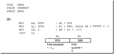
9.4.2 Memory Addressing Modes

The EU has direct access to all registers and data for register and immediate modes. However, the EU cannot directly access the memory operands. It must use the BIU to access memory operands. For example, when the EU needs a memory operand, it sends an offset value to the BIU. As mentioned before, this offset is added to the contents of a segment register after shifting it four times to the left, generating a 20-bit physical address. For example, suppose that the contents of a segment register is 2052 16 and the offset is 002016• Now, in order to generate the 20-bit physical address, the EU passes this offset to the BIU. The BIU then shifts the segment register four times to the left, obtains 20520 16 and then adds the 0020 16 offset to provide the 20-bit physical address 20540 16• Note that the 8086 must use a segment register whenever it accesses the memory.

Also, every memory addressing mode has a standard default segment register. However, a segment override instruction can be placed before most of the memory operand instructions whose default segment register is to be overridden. For example, INC BYTE PTR [START] will increment the 8-bit contents of a memory location in DS with offset START by 1. However, segment DS can be overridden byES as follows: INC ES: BYTE PTR [START ] . Segments cannot be overridden for stack reference instructions (such as PUSH and POP). The destination segment of a string segment, which must beES (if a prefix is used with a string instruction, only the source segment DS can be overridden) cannot be overridden. The code segment (eS) register used in program memory addressing cannot be overridden. The EU calculates an offset from the instruction for a memory operand. This offset is called the operand’s effective address, or EA. It is a 16-bit number that represents the operand’s distance in bytes from the start of the segment in which it resides.

The various memory addressing modes will now be described.

1. Memory Direct Addressing. In this mode, the effective address is taken directly from the displacement field of the instruction. No registers are involved. For example, MOV BX, [START], or MOV BX, OFFSET START moves the contents of the 20-bit address computed from DS and START to BX. Some assemblers use square brackets around START to indicate that the contents of the memory location(s) are at a displacement START from the segment DS. If square brackets are not used, then the programmer may define START as a 16-bit offset by using the assembler directive,
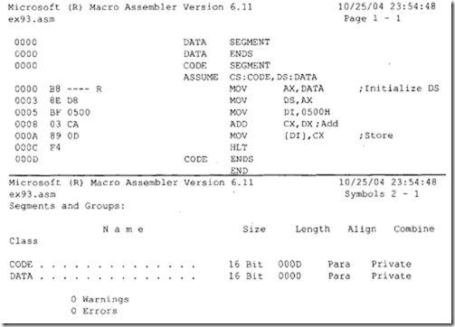
OFFSET.

2. Register Indirect Addressing. The effective address of a memory operand may be taken directly from one of the base or index registers (BX, BP, SI, DI). For example, consider MOV ex, [ BX l . If (DS) = 200016, (BX) = 0004 16, and (20004 16) = 022416, then, after MOV CX, [ BX], the contents of ex are 0224 16• Note that the segment register used in MOV ex, [ BX] can be overridden, such as MOV ex, ES: [ BX] . Now, the MOV instruction will use ES instead ofDS. If(ES) = 100016 and (10004 16) = 0002 16, then, after MOV ex,ES: [BX],the register CX will contain 0002 16• Note that in the above, symbol ( ) is used to indicate the contents of an 8086 register or a memory location.

3. Based Addressing. In this mode, the effective address is the sum of a displacement value (signed 8-bit or unsigned 16-bit) and the contents of register BX or BP. For example, MOV AX, 4 [BX]moves the contents ofthe 20-bit address computed from a segment register and BX + 4 into AX. The segment register is DS or SS. The content ofBX is unchanged. The displacement (4 in this case) can be unsigned 16-bit or signed 8-bit. This means that if the displacement is 8-bit, then the 8086 sign extends this to 16-bit. Segment register SS is used when the stack is accessed; otherwise, this mode uses segment register DS. When memory is accessed, the 20-bit physical address is computed from BX and DS. On the other hand, when the stack is accessed, the 20-bit physical address is computed from BP and SS. Note that BP may be considered as the user stack pointer while SP is the system stack pointer. This is because SP is used by some 8086 instructions (such as CALL subroutine) automatically. The based addressing mode with BP is a very convenient way to access stack data. BP can be used as a stack pointer in SS to access local variables. Consider the following instruction sequence (arbitrarily chosen to illustrate the use ofBP for stack):

image

4. Indexed Addressing. In this mode, the effective address is calculated from the sum of a displacement value and the contents of register SI or DI. For example, MOV AX, VALUE [SI] moves the contents of the 20-bit address computed from VALUE, SI and the segment register into AX. The segment register is DS. The content of SI is unchanged. The displacement (VALUE in this case) can be unsigned 16-bit or signed 8-bit. The indexed mode can be used to access a table.

5. Based Indexed Addressing. In this mode, the effective address is computed from the

sum of a base register (BX or BP), an index register (SI or DI), and a displacement. For example, MOV AX, 4 [BX][SI] moves the contents of the 20-bit address computed from the segment register and (BX) + (SI) + 4 into AX. The segment register is DS. The displacement can be unsigned 16-bit or signed 8-bit. This mode can be used to access two-dimensional arrays such as matrices.

6. String Addressing. This mode uses index registers. SI is assumed to point to the first byte or word of the source string, and DI is assumed to point to the first byte or word of the destination when a string instruction is executed. The SI or DI is automatically incremented or decremented to point to the next byte or word depending on DF. The default segment register for source is DS, and it may be overridden; the segment register used for the destination must be ES, and can not be overridden. An example is MOVS WORD. If (DF) = 0, (DS) = 3000 16, (SI) = 002016, (ES) 500016,(DI) = 0040 16,(30020) = 3016, (30021) = 0516,(50040) = 0616,and (50041) = 2016,then, after this MOVS, (50040) = 3016,(50041) = 0516, (SI) = 002216, and (DI) = 0042 16

9.4.3 Port Addressing

Two I/0 port addressing modes can be used: direct port and indirect port. In either case, 8- or 16-bit I/0 transfers must take place via AL or AX respectively .In direct port mode, the port number is an 8-bit immediate operand to access 256 ports. For example. IN AL, 0 2 moves the contents of port 02 to AL. In indirect port mode, the port number is taken from DX, allowing 64K bytes or 32K words of ports. For example, suppose (DX) = 0020, (port 0020) = 02 16, and (port 0021) = 0316• then, after IN AX, DX, register AX contains 0302 16• On the other hand, after IN AL, DX, register AL contains 02 16

9.4.4 Relative Addressing Mode

Instructions using this mode specify the operand as a signed 8-bit displacement relative to IP. An example is JNC sTART. This instruction means that if carry= 0, then IP is loaded with the current IP contents plus the 8-bit signed value of START; otherwise, the next instruction is executed.

An advantage of relative mode is that the destination address is specified relative to the address of the instruction after the conditional Jump instruction. Since the 8086 conditional Jump instructions do not contain an absolute address, the program can be placed anywhere in memory which can still be executed properly by the 8086. A program which can be placed anywhere in memory, and can still run correctly is called a "relocatable" program. It is a good practice to write relocatable programs.
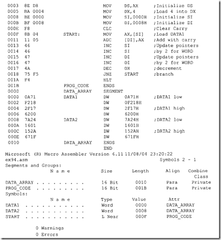
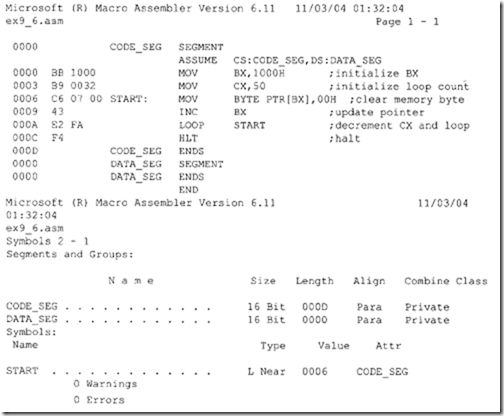
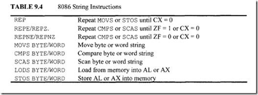
9.4.5 Implied Addressing Mode

Instructions using this mode have no operands. An example is CLC, which clears the carry flag to zero.