Process Transducers , Fluid Flow Transducers (Flowmeters) , Liquid Level Transducers and Temperature Transducers .

18.1.1 Process Transducers

This section discusses transducers used in measuring and controlling the process variables most frequently encountered in industrial processes, namely

Fluid pressure

Fluid flow

Liquid level

Temperature

Fluid Pressure Transducers

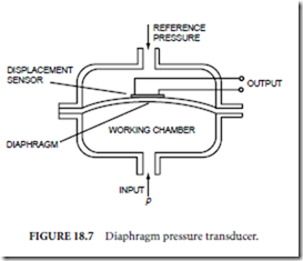
Most fluid pressure transducers are of the elastic type, in which the fluid is confined in a chamber with at least one elastic wall, and the deflection of the elastic wall is taken as an indication of the pressure. The Bourdon tube and the bellows are examples of elastic pressure transducers, which are used in laboratory-grade transducers and in some industrial process control applications. The fluid pressure transducer depicted in Fig. 18.7, which uses an elastic diaphragm to separate two chambers, is the type most frequently encountered in industrial process control. Diaphragms are constructed from one of a variety of elastic materials ranging from thin metal to polymerized fabric.

image

For gross pressure measurements, the displacement of the diaphragm is sensed by a potentiometer or LVDT; for more sensitive pressure measurements, any one of the three sensitive displacement sensors described earlier is used. In the most common configuration for sensitive pressure transducers, a strain gauge resistor with a rosette pattern is bonded to the diaphragm. In another configuration, the outer walls of the pressure sensor serve as capacitor plates and the diaphragm serves as the common plate of a differential capacitor. In a very sensitive and highly integrated configuration, the diaphragm is a silicon wafer with a piezoresistive strain gauge and signal conditioningcircuits integrated into silicon.

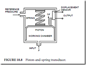
High-vacuum (very low pressure) measurements, usually based on observations of viscosity, thermal conductivity, acoustic properties, or ionization potential of the fluid, will not be included in this discussion. Transducers used in high-pressure hydraulic systems (70 MPa (10,000 psi) or greater) are usually of the piston and spring type (Fig. 18.8).

image

In either of the pressure transducers, the output is actually a measure of the difference in pressure between the working chamber and the reference chamber of the transducer (i.e., pOUT = p pREF). The measurement is called

✁ An absolute pressure if the reference chamber is sealed and evacuated (i.e., pREF = 0 and pOUT = p)

✁ A gauge pressure if the reference chamber is vented to the atmosphere (i.e., pOUT = p pATM)

✁ A differential pressure if any other pressure is applied to the reference chamber

Fluid Flow Transducers (Flowmeters)

Flowmetering, because of the number of variables involved, encompasses a wide range of measurement technology and applications. In industrial processes, the term fluid is applied not only to gases and liquids, but also to flowable mixtures (often called slurries or sludges) such as concrete, sewage, or wood pulp. Control of a fluid flow, and hence the type of measurement required, may involve volumetric flow rate, mass flow rate, or flow direction. Gas flows may be compressible, which also influences the measurement technique. In addition, the condition of the flow—whether or not it is homogenous and clean (free of suspended particles)—has a bearing on flowmeter technology. Another factor to be considered is flow velocity; slow moving laminar flows of viscous material require different measurement techniques than those used for high-velocity turbulent flows. Still another consideration is confinement of the flow. Whereas most fluid flow measurements are concerned with full flow through closed channels such as ducts and pipes, some applications require measurements of partial flow through open channels such as troughs and flumes. Only the most widely used flowmeters are considered here.

The major categories of flowmeters are

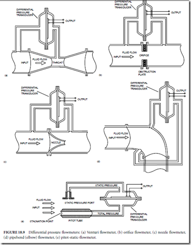
Differential pressure, constriction-type (venturi, orifice, flow nozzle, elbow (or pipe bend), and pitot static) (Fig. 18.9)

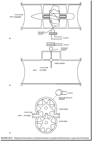
Fluid-power (gear motors, turbines and paddle wheels) (Fig. 18.10)

Ultrasound (Fig. 18.11)

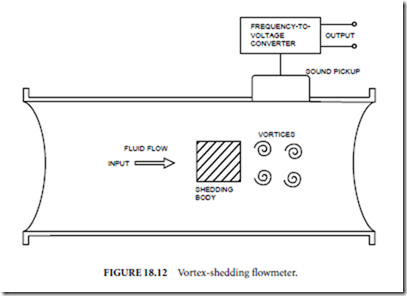
Vortex shedding (Fig. 18.12)

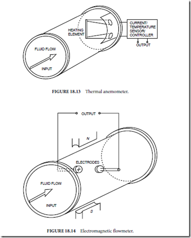
Thermal anemometer (Fig. 18.13)

Electromagnetic (Fig. 18.14)

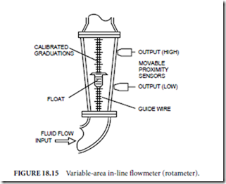
Rotameter (variable-area in-line flowmeter) (Fig. 18.15)

Differential pressure flowmeters are suited to high- and moderate-velocity flow of gas and clean, low- viscosity liquids. Venturi flowmeters (Fig. 18.9(a)) are the most accurate, but they are large and expensive. Orifice flowmeters (Fig. 18.9(b)) are smaller, less expensive, and much less accurate than venturi flowmeters. Nozzle flowmeters (Fig. 18.9(c)) are a compromise between venturi and orifice flowmeters. Pipe-bend flowmeters (Fig. 18.9(d)), which can essentially be installed in any bend in an existing piping system, are used primarily for gross flow rate measurements. Pitot-static flowmeters (Fig. 18.9(e)) are used in flows which have a large cross-sectional area, such as in wind tunnels. Pitot-static flowmeters are also used in freestream applications such as airspeed indicators for aircraft.

Fluid-power flowmeters are used in low-velocity, moderately viscous flows. In addition to industrial control applications, turbine flowmeters (Fig. 18.10(a)) are sometime used as speed indicators for ships or boats. Paddle wheel flowmeters (Fig. 18.10(b)) are used both in closed- and open-flow applications such as liquid flow in flumes. Since a fluid-power gear motor (Fig. 18.10(c)) is a constant volume device, motor shaft speed is always a direct indication of fluid flow rate.

Ultrasound flowmeters of the transmission type (Fig. 18.11(a)), which are based on the principle that the sound transmission speed will be increased by the flow rate of the fluid, are used in all types of clean, subsonic flows. Doppler flowmeters (Fig. 18.11(b)) rely on echoes from within the fluid, and are thus only useful in dirty flows that carry suspended particles or turbulent flows that produce bubbles. Ultrasound flowmeters are nonintrusive devices, which can often be retrofitted to existing duct or pipe systems.

Vortex shedding flowmeters (Fig. 18.12) introduce a shedding body into the flow to cause production (shedding) of vortices. The sound accompanying the production and collapse of the vortices is monitored and analyzed. The dominant frequency of the sound is indicative of the rate of vortex production and collapse, and hence an indication of flow rate. Vortex shedding flowmeters are useful in low-velocity, nonturbulent flows.

Thermal anemometers (Fig. 18.13) are used in low-velocity gas flows with large cross-sectional area, such as in heating, ventilation, and air conditioning (HVAC) ducts. Convection cooling of the heating element is related to flow rate. The flow rate measurement is based either on the current required to maintain a constant temperature in the heating element, or alternatively on the change in temperature when the current is held constant.

Electromagnetic flowmeters (Fig. 18.14) are useful for slow moving flows of liquids, sludges, or slurries. The flow material must support electrical conduction between the electrodes, and so in some cases it is necessary to ionize the flow upstream from the measurement point in order to use an electromagnetic flowmeter.

Variable-area in-line flowmeters (Fig. 18.15), or rotameters, are sometimes referred to as sight gauges because they provide a visible indication of flow rate. These devices, when fitted with proximity sensors (such as capacitive pickups), which sense the presence of the float, can be used in on-off control applications.

image

Liquid Level Transducers

Liquid-level measurements are relatively straightforward, and the transducers fall into the categories of contact or noncontact. Measurements may be continuous, in which the liquid level is monitored continuously throughout its operating range, or point, in which the liquid level is determined to be above or below some predetermined level.

image

image

image

image

image

image

The contact transducers encountered most frequently are

Float

Hydrostatic pressure

Electrical capacitance

Ultrasound

The noncontact transducers encountered most frequently are

Capacitive proximity sensors

Ultrasound

Radio frequency

Electro-optical

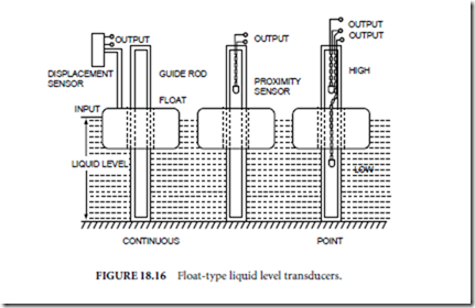
Float-type liquid level transducers are available in a wide variety of configurations for both continuous and point measurements. One possible configuration is depicted in Fig. 18.16 for continuous measurement and for both single- and dual-point measurements.

Hydrostatic pressure liquid level transducers may be used in either vented or pressurized applications (Fig. 18.17). In either case the differential pressure is directly proportional to the weight of the liquid column, since the differential pressure transducer accounts for surface pressure.

Capacitance probes (Fig. 18.18(a)) are widely used in liquid level measurements. It is possible, when the tank walls are metal, to use a single bare or insulated metal rod as one capacitor plate and the tank walls as the other. More frequently, capacitance probes consist of a metal rod within a concentric cylinder open at the ends, which makes the transducer independent of the tank construction. An interesting application of this type of capacitance probe is in aircraft fuel quantity indicators. Capacitance switches can be utilized as depicted in Fig. 18.18(b) to provide noncontact point measurements of liquid level.

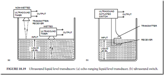
Ultrasound echo ranging transducers can be used in either wetted (contact) or nonwetted (noncontact) configurations for continuous measurement of liquid level (Fig. 18.19(a)). An interesting application of wetted transducers is as depth finders and fish finders for ships and boats. Nonwetted transducers can also be used with bulk materials such as grains and powders. Radio-frequency and electro-optic liquid level transducers are usually noncontact, echo ranging devices, which are similar in principle and application to the nonwetted ultrasound transducer.

Ultrasonic transducers can also be adapted to point measurements by locating the transmitter and the receiver opposite one another across a gap (Fig. 18.19(b)). When liquid fills the gap, attenuation of the

image

image

image

ultrasound energy is markedly less than when air fills the gap. The signal conditioning circuits utilize this sharp increase in the level of ultrasound energy detected by the receiver to activate a switch.

Temperature Transducers

Temperature measurement is generally based on one of the following physical principles:

Thermal expansion

Thermoelectric phenomena

Thermal effect on electrical resistance

Thermal effect on conductance of semiconductor junctions

Thermal radiation

(Strictly speaking, any device used to measure temperature may be called a thermometer, but more descriptive terms are applied to devices used in temperature control.)

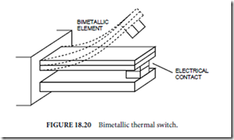
Bimetallic switches (Fig. 18.20) are widely used in on-off temperature control systems. If two metal strips with different coefficients of thermal expansion are bonded together while both strips are at the same temperature, the bimetallic structure will bend when the temperature is changed. Although these devices are often called thermal cutouts, implying that they are used in normally closed switches, they can be fabricated in either normally closed or normally open configurations. The bimetallic elements can also be fabricated in coil or helical configurations to extend the range of motion due to thermal expansion.

Thermocouples are rugged and versatile temperature sensors frequently found in industrial control systems. A thermocouple consists of a pair of dissimilar metal wires twisted or otherwise bonded at one end. The Seebeck effect is the physical phenomena which accounts for thermocouple operation, so thermocouples are known alternatively as Seebeck junctions. The potential difference (Seebeck voltage) between the free ends of the wire is proportional to the difference between the temperature at the junction and the temperature at the free ends. Thermocouples are available for measurement of temperature as low as −270◦C and as high as 2300◦C, although no single thermocouple covers this entire range. Thermocouples are identified as type B, C, D, E, G, J, K, N, R, S, or T, according to the metals used in the wire.

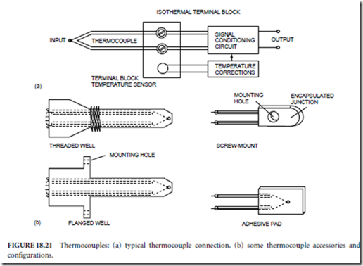
Signal conditioning and amplification of the relatively small Seebeck voltage dictates that the thermocouple wires must be connected to the terminals of a signal conditioning circuit. These connections create two additional Seebeck junctions, each of which generates its own Seebeck voltage, which must be canceled in the signal conditioning circuit. To implement cancellation to the corrections the following are necessary (Fig. 18.21(a)):

✁ The input terminals of the signal conditioning circuit must be made of the same metal.

✁ The two terminals must be on an isothermal terminal block so that each Seebeck junction created

by the connection is at the same temperature.

✁ The temperature of the terminal block must be known.

image

The first two requirements are met by appropriate construction of the signal conditioning circuit. The third requirement is met by using a reference temperature sensor, probably an IC temperature transducer of the type described later.

Thermocouple and thermocouple accessories are fabricated for a variety of applications (Fig. 18.21(b)). Protective shields are used to protect thermocouple junctions in corrosive environments or where con- ducting liquids can short circuit the thermocouple voltage; however, exposed (bare) junctions are used wherever possible, particularly when fast response is essential.

Resistance temperature detectors (RTDs) are based on the principle that the electrical resistivity of most metals increases predictably with temperature. Platinum is the preferred metal for RTDs, although other less expensive metals are used in some applications. The resistivity of platinum is one of the standards by which temperature is measured. The relatively good linearity of the resistivity of platinum over a wide temperature range (−200–800◦C) makes platinum RTDs suitable for stable, accurate temperature transducers, which are easily adapted to control systems applications.

The disadvantage of the RTD is that the temperature-sensitive element is a rather fragile metal filament wound on a ceramic bobbin or a thin metal film deposited on a ceramic substrate. RTD elements are usually encapsulated and are rarely used as bare elements. The accessories and application packages used with RTDs are similar to those used with thermocouples (Fig. 18.21(b)).

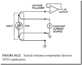
Most platinum RTDs are fabricated to have a nominal resistance of 100 Φ at 0◦C. The resistance temperature coefficient of platinum is approximately 3–4 mΦ/ Φ/◦C, so resolution of temperature to within 1◦C for a nominal 100-Φ RTD element requires resolution of the absolute resistance within 0.3–0.4 Φ. These resistance resolution requirements dictate use of special signal conditioning techniques to cancel the lead and contact resistance of the RTD element (Fig. 18.22). The circuit depicted in Fig. 18.22 is a variation of a 4-wire ohmmeter. Most RTDs are manufactured with four leads to be compatible with such circuits.

Thermistors are specially prepared metal oxide semiconductors that exhibit a strong negative temperature coefficient, in sharp contrast to the weak positive temperature coefficient of RTDs. Nominal thermistor resistance, usually specified for 25◦C, ranges from less than 1000 Φ to more than 1 MΦ, with sensitivities greater than 100 Φ/◦C. Thus, the thermistor is the basis for temperature sensors that are much more sensitive and require less special signal conditioning than either thermocouples or RTDs.

The tradeoff is the marked nonlinearity of the resistance-temperature characteristic. To minimize this problem, manufacturers provide packages in which the thermistor has been connected into a resistor network chosen to provide a relatively linear resistance-temperature characteristic over a nominal temperature range.

image


The development of thermistor technology has lead to the IC temperature sensor in which the temperature-sensitive junction(s) and the required signal conditioning circuits are provided in a monolithic package. The user is only required to provide a supply voltage (typically 5 V DC) to the IC in order to obtain an analog output voltage proportional to temperature. Thermistors and IC temperature sensors can be produced in very small packages, which permit highly localized temperature measurements.

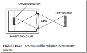
Some thermistors designed for biological research are mounted in the tip of a hypodermic needle. The shortcomings of both thermistor and IC temperature sensors are that they are not rugged, cannot be used in caustic environments, and are limited to temperatures below approximately 200◦C. Radiation thermometers are used for remote (non- contact) sensing of temperature in situations where the contact sensors cannot be used. Operation is based on the principles of heat transfer through thermal radiation. Radiation thermometers focus the infrared energy from a heat source onto a black body (target) within the radiation thermometer enclosure (Fig. 18.23). One of the contact temperature sensors described previously is incorporated into the target to measure the target temperature.

The rise in temperature at the target is related to the source temperature. Typical radiation thermometers have standoff ranges (focal lengths) of 0.5–1.5 m, but instruments with focal length as short as 1 cm or as long as 10 m are available. Radiation thermometers are available for broadband, monochromatic, or two-color thermometry.
image


Measurement Techniques: Sensors and Transducers , Introduction , Motion and Force Transducers , Displacement (Position) Transducers , Velocity Transducers and Acceleration Transducers

18.1 Measurement Techniques: Sensors and Transducers

18.1.1 Introduction

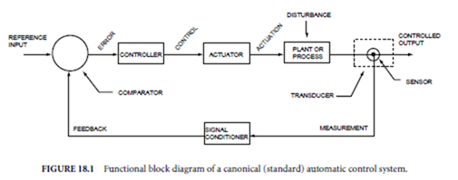
An automatic control system is said to be error actuated because the forward path components (comparator, controller, actuator, and plant or process) respond to the error signal (Fig. 18.1). The error signal is developed by comparing the measured value of the controlled output to some reference input, and so the accuracy and precision of the controlled output are largely dependent on the accuracy and precision with which the controlled output is measured. It follows then that measurement of the controlled output, accomplished by a system component called the transducer, is arguably the single most important function in an automatic control system.

image

A transducer senses the magnitude or intensity of the controlled output and produces a proportional signal in an energy form suitable for transmission along the feedback path to the comparator. (The term proportional is used loosely here because the output of the transducer may not always be directly proportional to the controlled output; that is, the transducer may not be a linear component. In linear systems, if the output of the transducer (the measurement) is not linear, it is linearized by the signal conditioner.) The element of the transducer which senses the controlled output is called the sensor; the remaining elements of a transducer serve to convert the sensor output to the energy form required by the feedback path. Possible configurations of the feedback path include

✁ Mechanical linkage

✁ Fluid power (pneumatic or hydraulic)

✁ Electrical, including optical coupling, RF propagation, magnetic coupling, or acoustic propagation

Electrical signals suitable for representing measurement results include

✁ DC voltage or current amplitude

✁ AC voltage or current amplitude, frequency, or phase (CW modulated)

✁ Voltage or current pulses (digital)

In some cases, representation may change (e.g., from a DC amplitude to digital pulses) along the feedback path.

The remainder of this discussion pertains to a large number of automatic control systems in which the feedback signal is electrical and the feedback path consists of wire or cable connections between the feedback path components. The transducers considered hereafter sense the controlled output and produce an electrical signal representative of the magnitude, intensity, or direction of the controlled output.

The signal conditioner accepts the electrical output of the transducer and transmits the signal to the comparator in a form compatible with the reference input. The functions of the signal conditioner include

• Amplification/attenuation (scaling)

• Buffering

• Isolation

• Digitizing

• Sampling

• Filtering

• Noise elimination

• Impedance matching

• Linearization

• Wave shaping

• Span and reference shifting

• Phase shifting

• Mathematical manipulation (e.g., differentiation, division, integration, multiplication, root finding, squaring, subtraction, or summation)

• Signal conversion (e.g., DC–AC, AC–DC, frequency–voltage, voltage–frequency, digital–analog, analog–digital, etc.)

In cases in which part or all of the required signal conditioning is accomplished within the transducer, the transducer output may be connected directly to the comparator. (Connection of the transducer output directly to the comparator should not be confused with unity feedback. Unity feedback occurs when the cascaded components of the feedback path (transducer and signal conditioner) have a combined transfer function equal to 1 (unity).) In a digital control system, many of the signal conditioning functions listed here can also be accomplished by software.

Transducers are usually considered in two groups:

Motion and force transducers, which are mainly associated with servomechanisms

Process transducers, which are mainly associated with process control systems

As will be seen, most process transducers incorporate some sort of motion transducer.

18.1.2 Motion and Force Transducers

This section discusses those transducers used in systems that control motion (i.e., displacement, velocity, and acceleration). Force is closely associated with motion, because motion is the result of unbalanced forces, and so force transducers are discussed concurrently. The discussion is limited to those transducers that measure rectilinear motion (straight-line motion within a stationary frame of reference) or angular motion (circular motion about a fixed axis). Rectilinear motion is sometimes called linear motion, but this leads to confusion in situations where the motion, though along a straight line, really represents a mathematically nonlinear response to input forces. Angular motion is also called rotation or rotary motion without ambiguity.

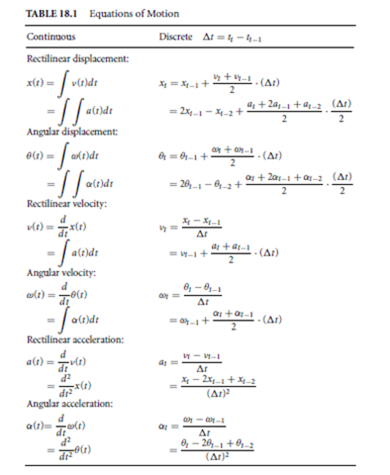
The primary theoretical basis for motion transducers is found in rigid-body mechanics. From the equations of motion for rigid-bodies (Table 18.1), it is clear that if any one of displacement, velocity, or

image

acceleration is measured, the other two can be derived by mathematical manipulation of the signal within an analog signal conditioner or within the controller software of a digital control system.

Position is simply a location within a frame of reference; thus, any measurement of displacement relative to the frame is a measurement of position, and any displacement transducer whose input is referenced to the frame can be used as a position transducer.

image

image

Displacement (Position) Transducers

Displacement transducers may be considered according to application as gross (large) displacement transducers or sensitive (small) displacement transducers. The demarcation between gross and sensitive dis- placement is somewhat arbitrary, but may be conveniently taken as approximately 1 mm for rectilinear

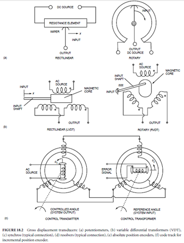
displacement and approximately 10 arc (1/6) for angular displacement. The predominant types of gross displacement transducers (Fig. 18.2) are

Potentiometers (Fig. 18.2(a))

Variable differential transformers (VDT) (Fig. 18.2(b))

Synchros (Fig. 18.2(c))

Resolvers (Fig. 18.2(d))

Position encoders (Fig. 18.2(e))

Potentiometer-based transducers are simple to implement and require the least signal conditioning, but potentiometers are subject to wear due to sliding contact between the wiper and the resistance element and may produce noise due to wiper bounce (Fig. 18.2(a)). Potentiometers are available with strokes ranging from less than 1 cm to more than 50 cm (rectilinear) and from a few degrees to more 50 turns (rotary).

VDTs are not as subject to wear as potentiometers, but the maximum length of the stroke is small, approximately 25 cm or less for a linear VDT (LVDT) and approximately 60◦ or less for a rotary VDT (RVDT). VDTs require extensive signal conditioning in the form of phase-sensitive demodulation of the AC signal; however, the availability of dedicated VDT demodulators in integrated circuit (IC) packages mitigates this disadvantage of the VDT.

Synchros are rather complex and expensive three-phase AC machines, which are constructed to be precise and rugged. Synchros are capable of measuring angular differences in the positions (up to ±180◦) of two continuously rotating shafts. In addition, synchros may function simultaneously as reference input, output measurement device, feedback path, and comparator (Fig. 18.2(c)).

Resolvers are simpler and less expensive than synchros, and they have an advantage over RVDTs in their ability to measure angular displacement throughout 360◦ of rotation. In Fig. 18.2(d), which represents one of several possibilities for utilizing a resolver, the signal amplitude is proportional to the cosine of the measured angle at one output coil and the sine of the measured angle at the other. Dedicated ICs are available for signal conditioning and for conversion of resolver output to digital format. The same IC, when used with a Scott-T transformer can be used to convert synchro output to digital format.

Position encoders are highly adaptable to digital control schemes because they eliminate the requirement for digital-to-analog conversion (DAC) of the feedback signal. The code tracks are read by track sensors, usually wipers or electro-optical devices (typically infrared or laser). Position encoders are available for both rectilinear and rotary applications, but are probably more commonly found as shaft encoders in rotary applications. Signal conditioning is straightforward for absolute encoders (Fig. 18.2(e)), requiring only a decoder, but position resolution depends on the number of tracks, and increasing the number of tracks increases the complexity of the decoder. Incremental encoders require more complex signal conditioning, in the form of counters and a processor for computing position. The number of tracks, however, is fixed at three (Fig. 18.2(f)). Position resolution is limited only by the ability to render finer divisions of the code track on the moving surface.

Although gross displacement transducers are designed specifically for either rectilinear or rotary motion, a rack and pinion, or a similar motion converter, is often used to adapt transducers designed for rectilinear motion to the measurement of rotary motion, and vice versa.

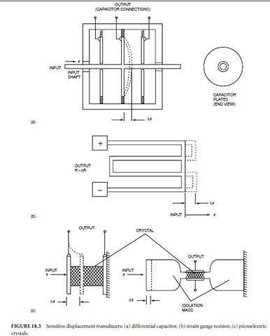
The predominant types of sensitive (small) displacement transducers (Fig. 18.3) are

Differential capacitors

Strain gauge resistors

Piezoelectric crystals

Figure 18.3(a) provides a simplified depiction of a differential capacitor used for sensitive displacement measurements. The motion of the input rod flexes the common plate, which increases the capacitance of one capacitor and decreases the capacitance of the other. In one measurement technique, the two capacitors are made part of an impedance bridge (such as a Schering bridge), and the change in the bridge output is an indication of displacement of the common plate. In another technique, each capacitor is allowed to serve as tuning capacitor for an oscillator, and the difference in frequency between the two oscillators is an indication of displacement.

A strain gauge resistor is used to measure elastic deformation (strain) of materials by bonding the resistor to the material (Fig. 18.3(b)) so that it undergoes the same strain as the material. The resistor is usually incorporated into one of several bridge circuits, and the output of the bridge is taken as an indication of strain.

image

The piezoelectric effect is used in several techniques for sensitive displacement measurements (Fig. 18.3(c)). In one technique, the input motion deforms the crystal by acting directly on one electrode. In another technique, the crystal is fabricated as part of a larger structure, which is oriented so that input motion bends the structure and deforms the crystal. Deformation of the crystal produces a small output voltage and also alters the resonant frequency of the crystal. In a few situations, the output voltage is taken directly as an indication of motion, but more frequently the crystal is used to control an oscillator, and the oscillator frequency is taken as the indication of strain.

image

Velocity Transducers

As stated previously, signal conditioning techniques make it possible to derive all motion measurements— displacement, velocity, or acceleration—from a measurement of any one of the three. Nevertheless, it is sometimes advantageous to measure velocity directly, particularly in the cases of short-stroke recti- linear motion or high-speed shaft rotation. The analog transducers frequently used to meet these two requirements are

Magnet-and-coil velocity transducers (Fig. 18.4(a))

Tachometer generators

A third category of velocity transducers, Counter-type velocity transducers (Fig. 18.4(b)), is simple to implement and is directly compatible with digital controllers.

The operation of magnet-and-coil velocity transducers is based on Faraday’s law of induction. For a solenoidal coil with a high length-to-diameter ratio made of closely spaced turns of fine wire, the voltage induced into the coil is proportional to the velocity of the magnet. Magnet-and-coil velocity transducers are available with strokes ranging from less than 10 mm to approximately 0.5 m.

A tachometer generator is, as the name implies, a small AC or DC generator whose output voltage is directly proportional to the angular velocity of its rotor, which is driven by the controlled output shaft. Tachometer generators are available for shaft speeds of 5000 r/min, or greater, but the output may be nonlinear and there may be an unacceptable output voltage ripple at low speeds.

AC tachometer generators are less expensive and easier to maintain than DC tachometer generators, but DC tachometer generators are directly compatible with analog controllers and the polarity of the output is a direct indication of the direction of rotation. The output of an AC tachometer generator must be demodulated (i.e., rectified and filtered), and the demodulator must be phase sensitive in order to indicate direction of rotation.

Counter-type velocity transducers operate on the principle of counting electrical pulses for a fixed amount of time, then converting the count per unit time to velocity. Counter-type velocity transducers rely on the use of a proximity sensor (pickup) or an incremental encoder (Fig. 18.2(f)). Proximity sensors may be one of the following types:

Electro-optic

Variable reluctance

Hall effect

Inductance

Capacitance

Two typical applications of counter-type velocity transducers are shown in Fig. 18.4(b).

Since a digital controller necessarily includes a very accurate electronic clock, both pulse counting and conversion to velocity can be implemented in software (i.e., made a part of the controller program).

Hardware implementation of pulse counting may be necessary if time-intensive counting would divert the controller from other necessary control functions. A special-purpose IC, known as a quadrature decoder/counter interface, can perform the decoding and counting functions and transmit the count to the controller as a data word.

Acceleration Transducers

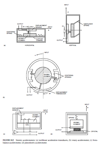
As with velocity measurements, it is sometimes preferable to measure acceleration directly, rather than derive acceleration from a displacement or velocity measurement. The majority of acceleration transducers may be categorized as seismic accelerometers because the measurement of acceleration is based on measuring the displacement of a mass called the seismic element (Fig. 18.5). The configurations shown in Fig. 18.5(a) and Fig. 18.5(b) require a rather precise arrangement of springs for suspension and centering of the seismic mass. One of the disadvantages of a seismic accelerometer is that the seismic mass is dis- placed during acceleration, and this displacement introduces nonlinearity and bias into the measurement. The force-balance configuration shown in Fig. 18.5(c) uses the core of an electromagnet as the seismic element. A sensitive displacement sensor detects displacement of the core and uses the displacement signal in a negative feedback arrangement to drive the coil, which returns the core to its center position. The output of the force-balance accelerometer is the feedback required to prevent displacement rather than displacement per se.

A simpler seismic accelerometer utilizes one electrode of a piezoelectric crystal as the seismic element (Fig. 18.5(d)). Similarly, another simple accelerometer utilizes the common plate of a differential capacitor (Fig. 18.3(a)) as the seismic element.

Force Transducers

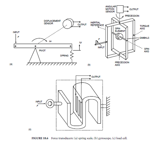
Force measurements are usually based on a measurement of the motion which results from the applied force. If the applied force results in gross motion of the controlled output, and the mass of the output element is known, then any appropriate accelerometer attached to the controlled output produces an output proportional to the applied force (F = Ma). A simple spring-balance scale (Fig. 18.6(a)) relies on measurement of displacement, which results from the applied force (weight) extending the spring.

Highly precise force measurements in high-value servomechanisms, such as those used in pointing and tracking devices, frequently rely on gyroscope precession as an indication of the applied force. The scheme is shown in Fig. 18.6(b) for a gyroscope with gimbals and a spin element. A motion transducer (either displacement or velocity) on the precession axis provides an output proportional to the applied force.

Other types of gyroscopes and precession sensors are also used to implement this force measurement technique.

Static force measurements (in which there is no apparent motion) usually rely on measurement of strain due to the applied force. Figure 18.6(c) illustrates the typical construction of a common force transducer called a load cell. The applied force produces a proportional strain in the S-shaped structural member, which is measured with a sensitive displacement transducer, usually a strain gauge resistor or a piezoelectric crystal.

image

image


QUESTIONS AND PROBLEMS

QUESTIONS AND PROBLEMS

11.1 Discuss the typical features of 32-bit and 64-bit microprocessors.

11.2

(a) What is the basic difference between the 80386 and 80386SX?

(b) What is the basic difference between the 80386 and 80486?

11.3 What is the difference between the 80386 protected, real-address, and virtual 8086 modes?

11.4 Discuss the basic features of the 80486.

11.5 Assume the following 80386 register contents

(EBX) = 00001000H

(ECX)=04000002H

(EDX) = 20005000H

prior to execution of each of the following 80386 instructions. Determine the contents of the affected registers and/or memory locations after execution of each of the following instructions and identify the addressing modes:

(a) MOV        [EBX * 4]        [ECX],         EDX

(b) MOV       [EBX * 2]        [ECX + 2020H],       EDX

11.6 Determine the effect of each of the following 80386 instructions:

(a) MOVZX      EAX,        CH

Prior to execution of this MOVZX instruction, assume

(EAX) = 80001234H

(ECX) = 00008080H

(b) MOVSX EDX, BL

Prior to execution of this MOVSX assume

(EDX) = FFFFFFFFH

(EBX) = 05218888H

11.7 Write an 80386 assembly program to add a 64-bit number in ECX: EDX with another 64-bit number in EAX: EBX. Store the result in EAX: EBX.

11.8 Write an 80386 assembly program to divide a signed 32-bit number in DX:AX by an 8-bit signed number in BH. Store the 16-bit quotient and 16-bit remainder in AX and DX respectively.

11.9 Write an 80386 assembly program to compute

image

where N = I 000 and the X;’s are signed 32-bit numbers.

Assume that LX? can be stored as a 32-bit number.

11.10 Discuss 80386 I/O.

11.11 Compare the on-chip hardware features of the 80486 and Pentium micro­ processors.

11.12 What are the sizes of the address and data buses of the 80486 and the Pentium?

11.13 Identify the main differences between the 80486 and the Pentium.

11.14 What are the clock speed, pipeline model, number of on-chip transistors, and number of pins on the 80486 and Pentium processors?

11.15 Discuss typical applications of Pentium.

11.16 Identify the main differences between the Intel80386 and 80486.

11.17 What is meant by the 80486 BUS BACKOFF feature?

11.18 How many pipeline stages are in Pentium and Pentium Pro?

11.19 How many new instructions are added to the 80486 beyond those of the 80386?

11.20 Given the following register contents,

(EBX) = 7F271 08AH

(ECX) = 2A157241H

what is the content of ECX after execution of the following 80486 instruction sequence:

MOV            EBX,ECX

BSWAP        ECX

BSWAP       ECX

BSWAP       ECX

BSWAP      ECX

11.21 If (EBX) = 0123A212H and (EDX) = 46B12310H, then what are the contents of EBX and EDX after execution of the 80486 instruction XADD EBX, EDX?

11.22 If (BX) = 271AH, (AX)= 712EH, and (CX) = 1234H, what are the contents of AX after execution of the 80486 instruction CMPXCHG ex, BX?

11.23 What are three modes of the Pentium processor? Discuss them briefly.

11.24 What is meant by the statement, "The Pentium processor is based on a superscalar design"?

11.25 What are the purposes of the U pipe and V pipe of the Pentium processor?

11.26 What are the sizes of the data and instruction caches in the Pentium?

11.27 Summarize the basic differences among Pentium, Pentium Pro, and Pentium II, Ce1eron, Pentium II Xeon, Pentium III, and Pentium III Xeon processors.

11.28 Why are the Pentium Pro’s complete capabilities not used by the Windows 95 operating system?

11.29 Summarize the basic features of the Intel/Hewlett-Packard "Merced" microprocessor.

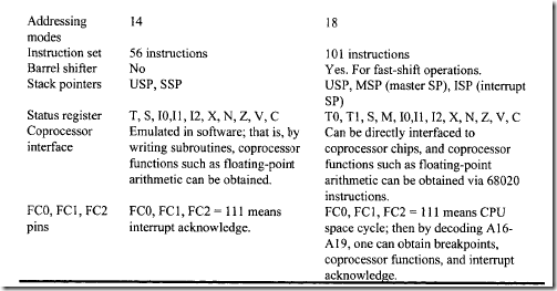
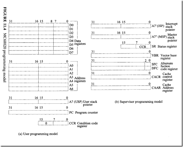
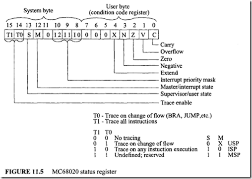
11.30 Summarize the basic differences between the 68000, 68020, 68030, 68040 and 68060.

11.31 What is the unique feature of the Power PC microprocessor family?

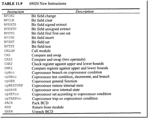
11.32 Name three new 68020 instructions that are not provided with the 68000.

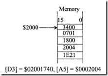
11.33 Find the contents of the affected registers and memory locations after execution of the 68020 instruction MOVE ( $10 0 0 , AS , D 3 .w * 4 ) , D 1.Assume the following data prior to execution of this MOVE:

[AS]= $0000F210, [$ 00014218] = $4567

[D3] = $00001002, [$ 0001421A] = $2345

[Dl] = $F125012A

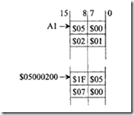
11.34 Assume the following 68020 memory configuration:

image

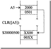
Find the contents of the affected memory locations after execution of MOVE .W #$1234, ( [Al]).

11.35 Find the 68020 compare instruction with the appropriate addressing mode to replace the following 68000 instruction sequence:

ASL.     L     #l,        D5

CMP. L  0  (AO I D5. L)  I  D0

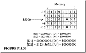
11.36 Find the contents of D I, D2, A4, and CCR and the memory locations after execution of each of the following 68020 instructions:

image

11.37 Identify the following 68020 instructions as valid or invalid. Justify your answers.

(a) DIVS A0, Dl

(b) CHK.B D0, (A0)

(c) MOVE.L D0, (A0)

It is given that [A0] = $1025671A prior to execution of the MOVE.

11.38 Determine the values of the Z and C flags after execution of each of the following 68020 instructions:

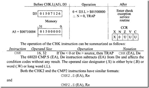
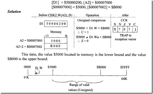
(a) CHK2. W (A5), D3

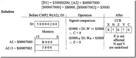
(b) CMP2. L $2001 I A5

Assume the following data prior to execution of each of these instructions:

image

11.39 Write a 68020 assembly program to add two 64-bit numbers in D1D0 with another 64-bit number in D2D3. Store the result in D1D0.

11.40 Write a 68020 assembly program to multiply a 32-bit signed number in D5 by another 16-bit signed number in D 1. Store the 64-bit result in D5B 1.

11.41 Write a subroutine in 68020 assembly language to compute image 

Assume the X1 ‘s are signed 32-bit numbers and the array starts at $50000021. Neglect overflow.

11.42 Write a program in 68020 assembly language to find the first one in a bit field which is greater than or equal to 16 bits and less than or equal to 512 bits. Assume that the number of bits to be checked is divisible by 16. If no ones are found, store zero in D3; otherwise store the offset of the first set bit in D3, and then stop. Assume A2 contains the starting address of the array, and D2 contains the number of bits in the array.

11.43 Write a program in 68020 assembly language to multiply a signed byte by a 32-bit signed number to obtain a 64-bit result. Assume that the numbers are respectively pointed to by the addresses that are passed on to the user stack by a subroutine pointed to by (A7+6) and (A7+8). Store the 64-bit result in D2:Dl.

11.44 What is meant by 68020 dynamic bus sizing?

11.45 Consider the 68020 instruction MOVE .B D 1,$ 0 0 0 0 0 0 16. Find the 68020 data pins over which data will be transferred if DSACK 1 DSACKO = 00. What are the 68020 data pins if DSACK l DSACKO = 10?

11.46 If a 32-bit data is transferred using 68020 MOVE. L DO, $50 6 0 7 011 instruction to a 32-bit memory with [DO]= $81F2756l, how many bus cycles are needed to perform the transfer? What are A 1A0 equal to during each cycle? What is the SIZ 1 SIZO code during each cycle? What bytes of data are transferred during each bus cycle?

11.47 Discuss 68020 I/O.

11.48 What do you mean by the unified cache of the 601? What is its size?

11.49 List the user-level and general-purpose registers of the 601.

11.50 Name one supervisor-level register in the 601. What is its purpose?

11.51 How does the 601 MSR indicate the following:

(a) The 601 executes both the user- and supervisor- level instructions.

(b) The 601 executes only the user-level instructions.

11.52 Explain the operation performed by each of the following 601 instructions:

(a) add.    r1,r2,r3

(b) divwu    r2,r3,r4

(c) extsb    r1,r2

11.53 Discuss briefly the exceptions included in the PowerPC 601.

11.54 Compare the basic features of the 601 with the 620. Discuss PowerPC 64-bit MP’s.

11.55 Summarize the basic features of Motorola’s state-of-the-art microprocessors.


Motorola’s State-of-the-art Microprocessors

11.7.2 Motorola’s State-of-the-art Microprocessors

As part of their plans to carry the PowerPC architecture into the future, Motorola /IBM/ Apple already announced AltiVec extensions for the PowerPC family. The result is the MPC7400 PowerPC microprocessor. This microprocessor is available in 400 MHz, 450 MHz and 500 MHz clock speeds. Motorola’s AltiVec technology is the foundation for the Velocity Engine of Apple Computer’s next generation desktop computers. For example, Apple rececently announced Power Mac G5 which uses Motorola’s 64-bit microprocessor, G5. AltiVec extensions are somewhat comparable to the MMX extensions in Intel’s Pentium family. AltiVec has independent processing units while Intel tied MMX to the floating-point unit. Both utilize SIMD (Chapter 8). A comparison of some of the features

of AltiVec vs. MMX is provided below:

image

In AltiVec, each processing unit can work independent of the others. This provides more parallelism by separate units. Since Intel tied MMX to floating-point unit, Pentiums can perform either floating-point math or switch over to MMX, but not both simultaneously. The switch requires a mode change that can cost hundreds of cycles, both going into and coming out ofMMX mode. It may be very tricky with Pentiums to write good and efficient codes when mixing of modes are required in some computing algorithms.

AltiVec can vetorize the floating-point operations. This means that one can use AltiVec to work on some data in the Floating-point Unit, then load the data in the AltiVec side (Vector Unit) without any significant mode switch. This may save hundreds of cycles . Also, this allows programmers to do more with the Vector Unit since they can go back and forth to mix and match.

The biggest drawback with MMX or AltiVec is getting programmers to use them. Programmers are required to use assembly language for MMX. Therefore, a few programmers used MMX for dedicated applications. For example, Intel hand tuned some photoshop filters for Adobe. Programmers can use C language with AltiVec. Therefore, it is highly likely that more programmers will use AltiVec than MMX.

In the future, Motorola and IBM plan to introduce the PowerPC series 2K. It is expected that the chip will contain 100 million transistors and have clock speeds greater than 1 GHz.


Motorola MC68030 , Motorola MC68040 I MC68060 , PowerPC Microprocessor , IBM/Motorola/Apple PowerPC 601 , PowerPC 601 Registers , PowerPC 601 Addressing Modes , Typical PowerPC 601 Instructions , Integer Instructions , Floating-Point Instructions , Load/Store Instructions , PowerPC 601 Exception Model , Summary of PowerPC 601 Features and PowerPC 64-Bit Microprocessors.

11.7.2 Motorola MC68030

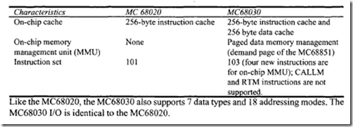
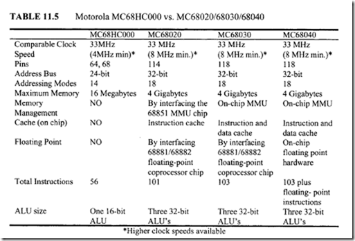
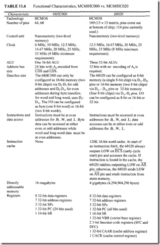
The MC68030 is a virtual memory microprocessor based on the MC68020 with additional features. The MC68030 is designed by using HCMOS technology and can be operated at clock rates of 16.67 and 33 MHz. The MC68030 contains all features of the MC68020, plus some additional ones. The basic differences between the MC68020 and MC68030 are as follows:

image

11.7.3 Motorola MC68040 I MC68060

This section presents an overview of the Motorola MC68040 and MC 68060 32-bit microprocessors. The MC68040 is Motorola’s enhanced 68030, 32-bit microprocessor, implemented in HCMOS technology. Providing balance between speed, power, and physical device size, the MC68040 integrates on-chip MC68030-compatible integer unit, an MC68881/ MC68882-compatible floating-point unit (FPU), dual independent demand­ paged memory management units (MMUs) for instruction and data stream accesses, and an independent 4 KB instruction and data cache. A high degree of instruction execution parallelism is achieved through the use of multiple independent execution pipelines, multiple internal buses, and separate physical caches for both instruction and data accesses. The MC68040 also includes 32-bit nonmultiplexed external address and data buses.

The MC68060 is a superscalar ( two instructions per cycle) 32-bit microprocessor. The 68060, like the Pentium, is designed using a combination of RISC and CISC architectures to obtain high performance. For some reason, Motorola does not offer MC68050 microprocessor. The 68060 is fully compatible with the 68040 in the user mode. The 68060 can operate at 50- and 66-MHz clocks with performance much faster than the 68040. An striking feature of the 68060 is the power consumption control. The 68060 is designed using static HCMOS to reduce power during normal operation.

11.7.4 PowerPC Microprocessor

This section provides an overview of the hardware, software, and interfacing features associated with the RISC microprocessor called the PowerPC. Finally, the basic features of both 32-bit and 64-bit PowerPC microprocessors are discussed

Basics of RISC

RISC is an acronym for Reduced Instruction Set Computer. This type of microprocessor emphasizes simplicity and efficiency. RISC designs start with a necessary and sufficient instruction set. The purpose of using RISC architecture is to maximize speed by reducing clock cycles per instruction. Almost all computations can be obtained from a few simple operations. The goal of RISC architecture is to maximize the effective speed of a design by performing infrequent operations in software and frequent functions in hardware, thus obtaining a net performance gain. The following summarizes the typical features of a RISC microprocessor:

1. The RISC microprocessor is designed using hardwired control with little or no microcode. Note that variable-length instruction formats generally require microcode design. All RISC instructions have fixed formats, so microcode design is not necessary.

2. A RISC microprocessor executes most instructions in a single cycle.

3. The instruction set of a RISC microprocessor typically includes only register, load, and store instructions. All instructions involving arithmetic operations use registers, and load and store operations are utilized to access memory.

4. The instructions have a simple fixed format with few addressing modes.

5. A RISC microprocessor has several general-purpose registers and large cache memones.

6. A RISC microprocessor processes several instructions simultaneously and thus includes pipelining.

7. Software can take advantage of more concurrency. For example, Jumps occur after execution of the instruction that follows. This allows fetching of the next instruction during execution of the current instruction.

RISC microprocessors are suitable for embedded applications. Embedded microprocessors or controllers are embedded in the host system. This means that the presence and operation of these controllers are basically hidden from the host system. Typical embedded control applications include office automation systems such as laser printers. Since a laser printer requires a high performance microprocessor with on-chip floating-point hardware, RISC microprocessors such as PowerPC are ideal for these types of applications.

RJSC microprocessors are well suited for applications such as image processing, robotics, graphics, and instrumentation. The key features of the RJSC microprocessors that make them ideal for these applications are their relatively low level of integration in the chip and instruction pipeline architecture. These characteristics result in low power consumption, fast instruction execution, and fast recognition of interrupts. Typical 32- and 64-bit RJSC microprocessors include PowerPC microprocessors.

IBM/Motorola/Apple PowerPC 601

This section provides an overview of the basic features of PowerPC microprocessors. The PowerPC 601 was jointly developed by Apple, IBM, and Motorola. It is available from IBM as PP 601 and from Motorola as MPC 601. The PowerPC 601 is the first implementation of the PowerPC family of Reduced Instruction Set Computer (RJSC) microprocessors. There are two types of PowerPC implementations: 32-bit and 64-bit. The PowerPC 601 implements the 32-bit portion of the IBM PowerPC architectures and Motorola 88100 bus control logic. It includes 32-bit effective (logical) addresses, integer data types of 8, 16, and 32 bits, and floating-point data types of 32 and 64 bits. For 64-bit PowerPC implementations, the PowerPC architecture provides 64-bit integer data types, 64-bit addressing, and other features necessary to complete the 64-bit architecture.

The 60 I is a pipelined superscalar processor and is capable of executing three instructions per clock cycle. A pipelined processor is one in which the processing of an instruction is broken down into discrete stages, such as decode, execute, and write-back (the result of the operation is written back in the register file).

Because the tasks required to process an instruction are broken into a series of tasks, an instruction does not require the entire resources of an execution unit. For example, after an instruction completes the decode stage, it can pass on to the next stage, and the subsequent instruction can advance into the decode stage. This improves the throughput of the instruction flow. For example, it may take three cycles for an integer instruction to complete, but if there are no stalls in the integer pipeline, a series of integer instructions can have a throughput of one instruction per cycle. Each unit is kept busy in each cycle.

A superscalarprocessor is one in which multiple pipelines are provided to allow instructions to execute in parallel. The PowerPC 60 I includes three execution units: a 32-bit integer unit (IU), a branch processing unit (BPU), and a pipelined floating-point unit (FPU).

The PowerPC 60 I contains an on-chip, 32 KB unified cache (combined instruction and data cache) and an on-chip memory management unit (MMU). It has a 64-bit data bus and a 32-bit address bus. The 601 supports single-beat and four-beat burst data transfer for memory accesses. Note that a single-beat transaction indicates data transfer of up to 64 bits. The PowerPC 601 uses memory-mapped I/O. Input/output devices can also be interfaced to the PowerPC 601 by using the I/O controller. The 60 I is designed by using an advanced, CMOS process technology and maintains full compatibility with TTL devices.

The PowerPC 601 contains an on-chip real-time clock (RTC). The RTC was normally an I/O device completely outside the CPU in earlier microcomputers. Although the RTC appearing inside the microcomputer chip is common on single-chip microcomputers, this is the first time the RTC is implemented inside a top-of-the-line microprocessor such as the PowerPC. This implication is that modem multitasking operating systems require time keeping for task switching as well as keeping the calendar date. The 601 real-time clock (RTC) on-chip hardware provides a measure of real time in terms of time of day and date, with a calendar range of 136.19 years.

To specify the ordering of four bytes (ABCD) within 32 bits, the 601 can use either the ABCD (big-endian) or DCBA (little-endian) ordering. The 601 big- or little­ endian modes can be selected by setting the LM bit (bit 28) in the HIDO register. Note that big-endian ordering (ABCD) assigns the lowest address to the highest-order eight bits of the multibyte data. On the other hand, little-endian byte ordering (DCBA) assigns the lowest address to the lowest order (rightmost) 8 bits of the multibyte data.

Note that Motorola 68XXX microprocessors support big-endian byte ordering whereas Intel 80XXX microprocessors support little-endian byte ordering.

PowerPC 601 Registers

PowerPC 601 registers can be accessed depending on the program’s access privilege level (supervisor or user mode). The privilege level is determined by the privilege level (PR) bit in the machine status register (MSR). The supervisor mode of operation is typically used by the operating system, and user mode is used by the application software. The PowerPC 601 programming model contains user- and supervisor-level registers. Some of these are

  •  The user-level register can be accessed by all software with either user or supervisor privileges.
  • The 32-bit GPRs (general-purpose registers, GPRO-GPR31) can be used as the data source or destination for all integer instructions. They can also provide data for generating addresses.
  • The 32-bit FPRs (floating-point registers, FPRO-FPR31) can be used as data sources and destinations for all floating-point instructions.
  • The floating-point status and control register (FPCSR) is a user control register in the floating-point unit (FPU). It contains floating-point status and control bits such as floating-point exception signal bits, exception summary bits, and exception enable bits.
  • The condition register (CR) is a 32-bit register, divided into eight 4-bit fields, CRO-CR7. These fields reflect the results of certain arithmetic operations and provide mechanisms for testing and branching.
  • The remaining user-level registers are 32-bit special purpose registers-SPR0, SPR1, SPR4, SPR5, SPR8, and SPR9.
  • SPRO is known as the MQ register and is used as a register extension to hold the product for the multiplication instructions and the dividend for the divide instructions. The MQ register is also used as an operand of long shift and rotate instructions.
  • SPRl is called the integer exception register (XER). The XER is a 32-bit register that indicates carries and overflow bits for integer operations. It also contains two fields for load string and compare byte indexed instructions.
  • SPR4 and SPR5 respectively represent two 32-bit read only registers and hold the upper (RTCU) and lower (RTCL) portions of the real-time clock (RTC). The RTCU register maintains the number of seconds from a time specified by software. The RTCL register maintains the fraction of the current second in nanoseconds. SPR8 is the 32-bit link register (LR). The link register can be used to provide the branch target address and to hold the return address after branch and link instructions.
  • SPR9 represents the 32-bit count register (CTR). The CTR can be used to hold a loop count that can be decremented during execution of certain branch instructions. The CTR can also be used to hold the target address for the branch conditional to count register instruction.

PowerPC 601 Addressing Modes

The effective address (EA) is the 32-bit address computed by the processor when executing a memory access or branch instruction or when fetching the next sequential instruction. Since the PowerPC is based on the RISC architecture, arithmetic and logical instructions do not read or modify memory.

Load and store operations have two types of effective address generation:

i) Register Indirect with Immediate Index Mode

Instructions using this mode contain a signed 16-bit index (d operand in the 32- bit instruction) which is sign extended to 32-bits, and added to the contents of a general­ purpose register specified by five bits in the 32-bit instruction (rA operand) to generate the effective address. A zero in the rA operand causes a zero to be added to the immediate index (d operand). The option to specify rA or 0 is shown in the instruction descriptions of the 601 user’s manual as the notation (rAIO).

An example is lbz rD,d (rA) where rA specifies a general-purpose register (GPR) containing an address, d is the the 16-bit immediate index and rD specifies a general­ purpose register as destination. Consider lb z r 1, 2 0 ( r 3) . The effective address (EA) is the sum r3+20. The byte in memory addressed by the EA is loaded into bits 31 through 24 of register rl. The remaining bits in rl are cleared to zero. Note that the registers r I and r3 represent GPR1 and GPR3 respectively.

ii) Register Indirect with Index Mode

Instructions using this addressing mode add the contents of two general-purpose registers (one GPR holds an address and another holds the index). An example is lbzx rD, rA, rB where rD specifies a GPR as destination, rA specifies a GPR as the index, and rB specifies a GPR holding an address. Consider lbzx rl, r4, r6. The effective address (EA) is the sum (r4IO)+(r6). The byte in memory adressed by the EA is loaded into register r 1 (24-31). The remaining bits in register rD are cleared to zero.

PowerPC 601 conditional and unconditional branch instructions compute the effective address (EA) or the next instruction address using various addressing modes A few of them are described below:

  • Branch Relative Branch instructions (32-bit wide) using the relative mode generate the address of the next instruction by adding an offset and the current program counter contents. An example of this mode is an instruction be start unconditionally jumps to the address PC + start.
  • Branch Absolute Branch instructions using this mode include the address of the next instruction to be executed. For example, the instruction ba begin unconditionally branches to the absolute address "begin" specified in the instruction.
  • Branch to Link Register Branch instructions using this mode branch to the address computed as the sum of the immediate offset and the address of the current instruction. The instruction address following the instruction is placed into the link register. For example, the instruction bl, start unconditionally jumps to the address computed from current PC contents plus start. The return address is placed in the link register.
  • Branch to Count Register Instructions using this mode branch to the address contained in the current register. Consider bet tr B0, BI means branch conditional to count register. This instruction branches conditionally to the address specified in the count register.

The BI operand specifies the bit in the condition register to be used as the condition of the branch. The B0 operand specifies how the branch is affected by or affects condition or count registers. Numerical values specifying BI and BO can be obtained from the 60 I manual.

Note that some instructions combine the link register and count register modes. An example is b cct r BO, B I .This instruction first performs the same operation as the bcttr and then places the instruction address following the instruction into the link register. This instruction is a form of "conditional call" because the return address is saved in the link register.

Typical PowerPC 601 Instructions

The 601 instructions are divided into the following categories:

1. Integer Instructions

2. Floating-point Instructions

3. Load/store Instructions

4. Flow Control Instructions

5. Processor Control Instructions

Integer instructions operate on byte (8-bit), half-word (16-bit), and word (32-bit) operands. Floating-point instructions operate on single-precision and double-precision floating-point operands.

Integer Instructions

The integer instructions include integer arithmetic, integer compare, integer rotate and shift, and integer logical instructions. The integer arithmetic instructions always set the integer exception register bit, CA, to reflect the carry out of bit 7. Integer instructions with the overflow enable (OE) bit set will cause the XER bits SO (summary overflow -overflow bit set due to exception) and OV (overflow bit set due to instruction execution) to be set to reflect overflow of the 32-bit result. Some examples of integer instructions are provided in the following. Note that rS, rD, rA, and rB in the following examples are 32-bit general purpose registers (GPRs) of the 601 and SIMM is 16-bit signed immediate number.

  • add rD, rA, SIMM performs the following immediate operation: rD +- (rAIO) + SIMM; rAIO) can be either (rA) or 0. An example is add rD, rA, SIMM or add rD, 0, SIMM.
  • add rD, rA, rB performs rD +- rA + rB.
  • add. rD, rA, rB adds with CR update as follows: rD +- rA + rB. The dot suffix enables the update of the condition register.
  • subf rD, rA, rB performs rD +- rB- rA.
  • sub r D, rA, r B performs the same operation as subf but updates the condition code register.
  • addme rD, rA performs the (add to minus one extended) operation: rD +- (rA) + FFFF FFFFH + CA bit in XER.
  • subfme rD, rA performs the (subtract from minus one extended) operation: rD +- (rA) + FFFF FFFFH + CA bit in XER, where (rA) represents the ones complement of the contents of rA.
  • mulhwu rD, rA, rB performs an unsigned multiplication of two 32-bit numbers in rA and rB. The high-order 32 bits of the 64-bit product are placed in rD.
  • mulhw rD, rA, rB performs the same operation as the mulhwu except that the multiplication is for signed numbers.
  • mullw rD, rA, rB places the low order 32-bits of the 64-bit product (rA)*(rB) into rD. The low-order 32-bit products are independent whether the operands are treated as signed or unsigned integers.
  • mulli rD, rA, SIMMplaces the low-order 32 bits of the 48-bitproduct(rA)*SIMM 16 into rD. The low-order bits of the 32-bit product are independent whether the operands are treated as signed or unsigned integers.
  • divw rD, rA, rB divides the 32-bit signed dividend in rA by the 32-bit signed divisor in rB. The 32-bit quotient is placed in rD and the remainder is discarded.
  • divwu rD, rA, rB is the same as the divw instruction except that the division is for unsigned numbers.
  • cmpi crfD, L, rA, SIMM compares 32 bits in rA with immediate SIMM treating operands as signed integer. The result of comparison is placed in crfd field (0 for CRO, I for CR 1, and so on) of the condition register. L=0 indicates 32-bit operands while L=l represents the 64-bit operands. For example, cmpi 0, 0, rA, 2 0 0 compares 32 bits in register rA with immediate value 200 and CRO is affected according to the comparison.
  • xor rA, rS, rB performs exclusive-or operation between the contents ofrS and rB. The result is placed into register rA.
  • extsb rA, rS places bits 24-31 ofrS into bits 24-31 ofrA. Bit 24 ofrS is then sign extended through bits 0-23 of rA.
  • slw rA, rS, rB shifts the contents ofrS left by the shift count specified by rB [27- 31]. Bits shifted out of position 0 are lost. Zeros are placed in the vacated positions on the right. The 32-bit result is placed into rA.
  • s rw rA, r S , r B is similar to s 1w r A, r S, r B except that the operation is for right shift.

Floating-Point Instructions

Some of the 601 floating-point instructions are provided below:

  • fadd frD, frA, frB adds the contents of the floating-point register, fr A to the contents of the floating-point register frB. If the most significant bit of the resultant significand is not a one, then the result is normalized. The result is rounded to the specified position under control of the FPSCR register. The result is rounded to the specified precision under control of the FPSCR register. The result is then placed in frD.

Note that this fadd instruction requires one cycle in execute stage, assuming normal operations; however, there is an execute stage delay of three cycles if the next instruction is dependent.

The 601 floating point addition is based on "exponent comparison and add by one" for each bit shifted, until the two exponents are equal. The two significands are then added algebraically to form an intermediate sum. If a carry occurs, the sum’s significand is shifted right one bit position and the exponent is increased by one.

  • f sub f r D, f rA, f r B performs frA – frB, normalization, and rounding of the result are performed in the same way as the f add instruction.
  • fmul frD1 frA 1 frC performs frD– frA * frC.Normalization and rounding of the result are performed in the same way as the fadd. Floating-point multiplication is based on exponent addition and multiplication of the significands.
  • fdiv frD , frA , frB performs the floating-point division frD — frNfrB. No remainder is provided. Normalization and rounding of the result are performed in the same way as the fadd instruction.
  • fmsub frDI frA1 FrC 1 frB performs frD <— frA * frC- frB. Normalization and rounding of the result are performed in the same way as the fadd instruction.

Load/Store Instructions

Some examples of the 60 I load and store instructions are

  • lhzx rD 1 rA 1 rB loads the half word (16 bits) in memory addressed by the sum (rAfO) + (rB) into bits 16 through 31 of rD. The remaining bits of rD are cleared to zero.
  • sthux rS 1 rA 1 rB stores the 16-bit halfword from bits 16-31 of register rS in memory addressed by the sum (rAfO) + (rB). The value (rAfO) + rB is placed into register rA.
  • lmw rD , d ( rA) loads n (where n = 32- D and D = 0 through 31) consecutive words starting at memory location addressed by the sum (r/0) + d into the general-purpose register specified by rD through r31.
  • stmu rS 1 d ( rA) is similar to lmw except that stmw stores n consecutive words.

Flow Control Instructions

Flow control instructions include conditional and unconditional branch instructions. An example of one of these instructions is

  • be (branch conditional) BO 1 BI 1 target branch with offset target if the condition bit in CR specified by bit number BI is true (The condition "true" is specified by a value inBO).

For example, be 12 1 0 1 target means that branch with offset target if the condition specified by bit 0 in CR (BI = 0 indicates the result is negative) is true (specified by the value BO = 12 according to Motorola PowerPC 601 manual).

Processor Control Instructions

Processor control instructions are used to read from and write to the machine state register (MSR), condition register (CR), and special status register (SPRs). Some examples of these instructions are

  • mfer rD places the contents of the condition register into rD.
  • mtmsr rS places the contents of rS into the MSR. This is a supervisor-level instruction.
  • mfimsr rD places the contents of MSR into rD. This is a supervisor-level instruction.

PowerPC 601 Exception Model

All 601 exceptions can be described as either precise or imprecise and either synchronous or asynchronous. Asynchronous exceptions are caused by events external to the processor’s execution. Synchronous exceptions, on the other hand, are handled precisely by the 601 and are caused by instructions; precise exception means that the machine state at the time the exception occurs is known and can be completely restored. That is, the instructions that invoke trap and system call exceptions complete execution before the exception is taken. When exception processing completes, execution resumes at the address of the next instruction.

An example of a maskable asynchronous, precise exception is the external interrupt. When an asynchronous, precise exception such as the external interrupt occurs, the 601 postpones its handling until all instructions and any exceptions associated with those instructions complete execution. System reset and machine check exceptions are two nonrnaskable exceptions that are asynchronous and imprecise. These exceptions may not be recoverable or may provide a limited degree of recoverability for diagnostic purpose.

Asynchronous, imprecise exceptions have the highest priority with the synchronous, precise exceptions having the next priority and the asynchronous, precise exceptions the lowest priority.

The 601 exception mechanism allows the processor to change automatically to supervisor state as a result of exceptions. When exceptions occur, information about the state of the processor is saved to certain registers rather than in memory as is usually done with other processors in order to achieve high speeds. The processor then begins execution at an address (exception vector) predetermined for each exception. The exception handler at the specified vector is then processed with processor in supervisor mode.

601 System Interface

The pins and signals of the PowerPC 601 include a 32-bit address bus and 52 control and information signals. Memory access allows transfer sizes of 8, 16, 24, 32, 40, 48, 56, or 64 bits in one bus clock cycle. Data transfer occurs in either single-beat transactions or four-beat burst transactions. Both memory and I/O accesses can use the same bus transfer protocols. The 601 also has the ability to define memory areas as I/O controller interface areas. The 601 uses the TS pin for memory-mapped accesses and the XATS pin for I/O controller interface accesses.

Summary of PowerPC 601 Features

The PowerPC 601 is a RlSC-based superscalar microprocessor. That is, it can execute two or more instructions per cycle. The PowerPC 601 is based on load/store architectures. This means that all instructions that access memory are either loads or stores, and all operate instructions are from register to register. Both load and store instructions have 32-bit fixed­ length instructions along with 32-bit integer and 32-bit floating-point registers.

The PowerPC 601 includes two primary addressing modes: register plus

displacement and register plus register. In addition, the 601 load and store instructions perform the load or store operation and also modify the index register by placing the effective address just computed. In the PowerPC 60 I, Branch target addresses are normally determined by using program counter relative mode. That is, the branch target address is determined by adding a displacement to the program counter. However, as mentioned before, conditional branches in the 601 may test fields in the condition code register and the contents of a special register called the count register (CTR). A single 601 branch instruction can implement a loop-closing branch by decrementing the CTR, testing its value, and branching if it is nonzero.

The PowerPC 601 saves the return address for certain control transfer instructions such as subroutine call in a general-purpose register. The 601 does this in any branch by setting the link (LK) bit to one. The return address is saved in the link register. The PowerPC 601 utilizes sophisticated pipelines. The 601 uses relatively short independent

image

pipelines with more buffering. The 601 does a lot of computation in each pipe stage. The 601 has a unified (combined) 32 KB cache. That is, instructions and data reside in the same cache in the 60 l. Finally, the 601 offers high performance by utilizing sophisticated design tricks. For example, the 601 includes powerful instructions such as floating-point multiply­ add and update load/store that perform more tasks with fewer instructions.

PowerPC 64-Bit Microprocessors

PowerPC 64-bit microprocessors include the PowerPC 620, 603e, 750/740, and 604e. These microprocessors are 64-bit superscalar processors. This means that they can execute more than one instruction in a cycle. Table 11.14 compares the basic features of the 32-bit PowerPC 601 with the 64-bit PowerPC 620.

There are a few versions of the 64-bit PowerPC available: PowerPC 603e, PowerPC 750/740, and PowerPC 604e. The PowerPC 603e microprocessor is available at speeds of 250, 275, and 300 MHz. The 603e has high performance and low power consumption, which makes it suited for applications found in the embedded system market. The PowerPC 603e is used in the Power Macintosh C500 series, which offers features such as accelerated multimedia, advanced video capture, and publishing. The PowerPC 750/740 is available at speeds up to 266 MHz and uses only 5 watts of power. The unique features offered by this microprocessor are built-in power-saving modes, an on-chip thermal sensor to regulate processor temperature, and a choice of packaging configurations. The PowerPC 604e microprocessor, another member of the PowerPC family, provides speeds of 350 MHz and using 8.0 watts of power. Like Intel, Motorola used the 0.25 micron process technology to achieve this speed. The PowerPC 604e is intended for high-end Macintosh and Mac-compatible systems.

Apple Computer’s original G3 (Marketing name used by Apple) utilized PowerPC 750 for Apple’s iMac and Power Macintosh personal computers. Apple’s G3 (later version) used Motorola’s copper-based PowerPC microprocessor, providing speed of up to 400 MHz.


MC68HC000 Enhanced Instructions and M68020 Pins and Signals

Example 11.8

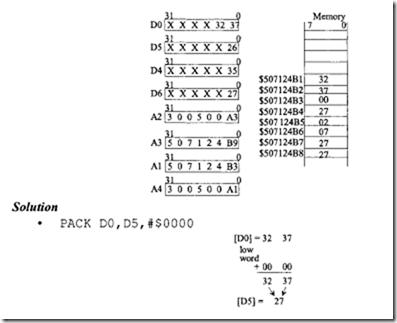
Determine the effect of execution of each of the following

PACK and UNPK instructions:

image

Assume the following data prior to execution of each of the above instructions:

image

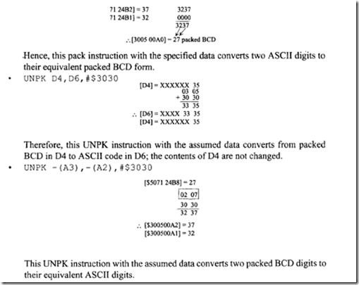
Note that ASCII code for 2 is $32 and for 7 is $37. Hence, this pack·instruction converts ASCII code to packed BCD.

PACK -(Al),-(A4),$0000

image

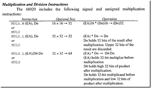
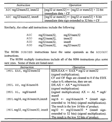
image(EA) can use all modes except An. The condition codes N: Z. and V are affected; C is always cleared to 0, and X is unaffected for both MULS and MULU. For signed multiplication, overflow (V = I) can only occur for 32 x 32 multiplication, producing a 32-bit result if the high-order 32 bits of the 64-bit product are not the sign extension of the low-order 32 bits. In the case of unsigned multiplication, overflow (V = I) can occur for 32 x 32 multiplication, producing a 32-bit result if the high-order 32 bits of the 64-bit product are not zero.

Both MULS and MULU have a word form and a long word form. For the word form ( 16 x 16), the multiplier and multiplicand are both 16 bits and the result is 32 bits. The result is saved in the destination data register. For the long word form (32 x 32), the multiplier and multiplicand are both 32 bits and the result is either 32 bits or 64 bits. When the result is 32 bits for a 32-bit x 32-bit operation, the low-order 32 bits of the 64-bit product are provided.

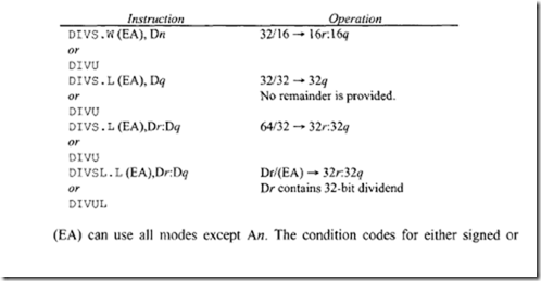
The signed and unsigned division instructions of the 68020 include the following, in which the source is the divisor, the destination is the dividend.

image

unsigned division are affected as follows: N = 1 if the quotient is negative; N = 0 otherwise. N is undefined for overflow or divide by zero. Z = 1 if the quotient is zero; Z = 0 otherwise. Z is undefined for overflow or divide by zero. V = 1 for division overflow; V = 0 otherwise. X is unaffected. Division by zero causes a trap. If overflow is detected before completion of the instruction, V is set to 1, but the operands are unaffected.

Both signed and unsigned division instructions have a word form and three long word forms. For the word form, the destination operand is 32 bits and the source operand is 16 bits. The 32-bit result in Dn contains the 16-bit quotient in the low word and the 16- bit remainder in the high word. The sign of the remainder is the same as the sign of the dividend.

For the instruction

imagethe destination is 64 bits contained in any two data registers and the source is 32 bits. The 32-bit register Dr (D0-D7) contains the 32-bit remainder and the 32-bit register Dq (D0-D7) contains the 32-bit quotient.

For the instruction

imagethe 32-bit register Dr (D0-D7) contains the 32-bit dividend and the source is also 32 bits. After division, Dr contains the 32-bit remainder and Dq contains the 32-bit quotient.

Example 11.9

Determine the effect of execution of each of the following multiplication and division instructions:

  • MULU. L # $2, D5 if [D5] = $FFFFFFFF
  • MULS. L  #$2,D5 if [D5] = $FFFFFFFF
  • MULU. L # $2,D5: D2 if [D5] = $2ABC 1800 and [D2] = $FFFFFFFF
  • DIVS.L     #$2,D5 if[D5]=$FFFFFFFC
  • DIVS. L    #$2, 02: D0 if [D2] = $FFFFFFFF and [D0]= $FFFFFFFC
  • DIVSL. L #$2, D6: D1 if [D1] = $00041234 and [D6] = $FFFFFFFD

Solution

  • MULU.L #$2,D5if[D5]=$FFFFFFFF

image

Therefore, [D5] = $FFFFFFFE, N = 0 since the most significant bit of the result is 0, Z = 0 because the result is nonzero, V = 1 because the high 32 bits of the 64-bit product are not zero, C = 0 (always), and X is not affected.

  • MULS.L #$2,D5 if[D5]=$FFFFFFFF

image

MC68HC000 Enhanced Instructions

The MC68020 includes the enhanced version of the instructions as listed next:

image

Note that Scan be B, W, or L. In addition to 8- and 16-bit signed displacements for BRA, Bee, and BSR like the 68HC000, the 68020 also allows signed 32-bit displacements. LINK is unsized in the 68HC000. (EA) in CMPI and TST supports all 68HC000 modes plus PC relative. An example is CMPI.W #$2000, (START, PC). In addition to EXT.W Dn and EXT.L Dn like the 68HC000, the 68020 also provides an EXTB.L instruction.

Example 11.10

Write a program in 68020 assembly language to multiply a 32-bit signed number in D2 by a 32-bit signed number in D3 by storing the multiplication result in the following manner:

(a) Store the 32-bit result in D2.

(b) Store the high 32 bits of the result in D3 and the low 32 bits of the result in D2.

Solution

image

Example 11.11

Write a program in 68020 assembly language to convert 10 packed BCD bytes (20 BCD digits) stored in memory starting at address $00002000 and above, to their ASCII equivalents and, store the result in memory locations starting at $FFFF8000.

Solution

image

M68020 Pins and Signals

The 68020 is arranged in a 13 x 13 matrix array ( 114 pins defined) and fabricated in a pin grid array (PGA) or other packages such as RC suffix package. Both the 32-bit address (A0-A31) and data (D0-D31) pins of the 68020 are nonmultiplexed. The 68020 transfers data

image

with an 8-bit device via D31-D24,with a 16-bit device via D16-D31,and with a 32-bit device via D31-D0• Figure 11.6 shows the MC68020 functional signal group. Table 11.11 lists these signals along with a description of each. There are 10 Vcc (+5 V) and 13 ground pins to distribute power in order to reduce noise.

Like the MC68HC000, the three function code signals FC2, FC 1, and FCO identify the processor state (supervisor or user) and the address space of the bus cycle currently being executed except that the 68020 defines the CPU space cycle as follows:

image

Note that in the 68HC000, FC2, FCl, FC0 = 111 indicates the interrupt acknowledge cycle. In the MC68020, it indicates the CPU space cycle. In this cycle, by decoding the address Jines A 19-A16, the MC68020 can perform various types of functions such as coprocessor communication, breakpoint acknowledge, interrupt acknowledge, and module operations as follows:

image

image

At the start of a bus cycle, the 68020 always transfers data to lines D0-D31, taking into consideration that the memory or I/O device may be 8, 16, or 32 bits wide. After the first bus cycle, the 68020 knows the device size by checking the DSACK0 and DSACKI pins and generates additional bus cycles if needed to complete the transfer.

Unlike the 68HC000, the 68020 permits word and long word operands to start at an odd address. However, if the starting address is odd, additional bus cycles are required to complete the transfer. For example, for a 16-bit device, the 68020 requires 2 bus cycles for a write to an even address such as MOVE . L D 1, $ 4 0 0 0 2 0 50 to complete the operation. On the other hand, the 68020 requires 3 bus cycles for MOVE . L D 1, $4 0 0 0 2 0 51 for a 16-bit device to complete the transfer. Note that, as in the 68HC000, instructions in the 68020 must start at even addresses.

Next, consider an example of dynamic bus sizing. The four bytes of a 32-bit data can be defined as follows:

image

If this data is held in a data register Dn and is to be written to a memory or I/O location, then the address lines A 1 and A0 define the byte position of data. For a 32-bit device, A 1A0 = 00 (addresses 0, 4, 8, ……), A 1A0 = 01 (addresses 1, 5, 9, …), A 1A0 = 10 (addresses 2, 6, 10, …),and A 1A0 =II (addresses 3, 7, II, …) will store OPO, OPI, OP2, and OP3, respectively. This data is written via the 68020 D31-D0 pins. However, if the device is 16-bit, data is always transferred as follows:

All even-addressed bytes via pins D31-D24 .

All odd-addressed bytes via pins D23-D16.

Finally, for an 8-bit device, both even- and odd-addressed bytes are transferred via pins D31-D24·

The 68020 always starts transferring data with the most significant byte first. As an example, consider MOVE . L D 1, $ 2 0 10 7 4 2 0. In the first bus cycle, the 68020 does not know the size of the device and, hence, outputs all combinations of data on pins D31-D0, taking into consideration that the device may be 8, 16, or 32 bits wide. Assume that the content of Dl is $02Al0512 (OPO = $02, OPI =$AI, OP2 = $05, and OP3 = $12). In the first bus cycle, the 68020 sends SIZl SIZO = 00, indicating a 32-bit transfer, and then outputs data on its D31-D0 pins as follows:

image

If the device is 8-bit, it will take data $02 from pins D31-D24 in the first cycle and will then assert DSACKI and DSACKO as 10, indicating an 8-bit device. The 68020 then transfers the remaining 24 bits ($A 1 first, $05 next, and $12 last) via pins D31-D24 in three consecutive cycles, with a total of four cycles being necessary to complete the transfer.

However, if the device is 16-bit, in the first cycle the device will take the 16-bit data $02Al via pins D31-D16 and will then assert DSACKI and DSACKO as 01, indicating a 16-bit device. The 68020 then transfers the remaining 16 bits ($0512) via pins D31-D16 in the next cycle, requiring a total of two cycles for the transfer.

Finally, if the device is 32-bit, the device receives all 32-bit data $02A 10512 via pins D31-D0 and asserts DSACKI DSACKO = 00 to indicate completion of the transfer. Aligned data transfers for various devices are as follows :

For 8-bit device:

image

Let us explain some of the other 68020 pins.

The ECS (external cycle start) pin is an MC68020 output pin. The MC68020 asserts this pin during the first one half clock of every bus cycle to provide the earliest indication of the start of a bus cycle. The use of ECS must be validated later with AS, because the MC68020 may start an instruction fetch cycle and then abort it if the instruction is found in the cache. In the case of a cache hit, the MC68020 does not assert AS, but provides A31-A0, SIZl, SIZO, and FC2-FCO outputs.

The MC68020 AVEC input is activated by an external device to service an autovector interrupt. The AVEC has the same function as VPA on the 68HC000. The functions of the other signals, such as AS, RJW, IPL2- IPLO, BR, BG, and BGACK, are similar to those of the MC68HC000.

The MC68020 system control pins are functionally similar to those of the MC68HC000. However, there are some minor differences. For example, for hardware reset, RESET and HALT pins need not be asserted simultaneously. Therefore, unlike the 68HC000, the RESET and HALT pins are not required to be tied together in the MC68020 system.

The RESET and HALT pins are bidirectional and open drain (external pull-up resistances are required), and their functions are independent. The RESET signal is a bidirectional signal. The RESET pin, when asserted by an external circuit for a minimum of 520 clock periods, the RESET pin resets the entire system including the MC68020. Upon hardware reset, the MC68020 completes any active bus cycle in an orderly manner and then performs the following:

  • Reads the 32-bit content of address $00000000 and loads it into the ISP (the contents of $00000000 are loaded to the most significant byte of the ISP and so on).
  • Reads the 32-bit contents of address $00000004 into the PC (contents of $00000004 to most significant byte of the PC and so on).
  • Sets the 12 11 10 bits of the SR to 1 1 1, sets the S bit in the SR to 1, and clears the T1 , T0, and M bits in the SR.
  • Clears the VBR to $00000000.
  • Clears the cache enable bit in the CACR.
  • All other registers are unaffected by hardware reset.

When the RESET instruction is executed, the MC68020 asserts the RESET pin for 512 clock cycles and the processor resets all the external devices connected to the RESET pin. Software reset does not affect any internal register.

As mentioned earlier while describing dynamic bus sizing, the 68020 always drives all data lines during a write operation. Furthermore, for all inputs there is a sample window of at least 20 ns during which the 68020 latches the input level. To guarantee the recognition of a certain level on a particular falling edge of the clock, the input level must be held stable throughout this sample window, 20 ns; otherwise, the level recognized by the MC68020 is unknown or legal.

During data transfer operations, the 68020 can use either synchronous or asynchronous operation. In synchronous operation, the 68020 clock is used to generate DSACK1, DSACK0, and other asynchronous inputs. Also, in synchronous operation, if the DSACKl and DSACK0 are asserted for the required window of at least 20 ns (at least 5 ns before and at leastl5 ns after the falling edge of S2) on the falling edge S2, the 68020 latches valid data on the falling edge of S4 on a read cycle. The 68020 does not generate any wait states if DSACK1 and DSACK0 are asserted at the falling edge ofS2; otherwise the 68020 inserts wait cycles like the 68HC000 and latches data at the falling edge of the following cycle as soon as DSACK1 and DSACK0 are asserted. A minimum of three clock cycles are required for a read operation.

In asynchronous operation, clock frequency independence at a system level is achieved and the 68020 is used in an asynchronous manner. This typically requires using the bus signals such as AS, DS, DSACKI, and DSACKO to control data transfer. Using asynchronous operation, AS starts the bus cycle and DS is used as a condition of valid data on a write cycle. Decoding of SIZ 1, SIZO, A 1, and A0 provides enable signals, which indicate the portion of the data bus that is used in data transfer. The memory or I/O chip then responds by placing the requested data on the correct portion of the data bus for a read cycle or latching the data on a write cycle and asserting DSACK1, and DSACKO, corresponding to the memory or I/O port size (8-bit, 16-bit, or 32-bit), to terminate the bus cycle. If no memory or I/O device responds or the address is invalid, the external control logic asserts the BERR or BERR and HALT signal(s) to abort or retry the bus cycle or retries the bus cycle.

In asynchronous operation, the DSACKI, and DSACKO signals are allowed to be asserted before the data from memory or an I/O device is valid on a read cycle. The 68020 latches data according to Parameter #31 provided in Motorola manuals. (Parameter #31 is a maximum of 60 ns for the 12.5-MHz 68020, a maximum of 50 ns for the 16.67-MHz 68020, and a maximum of 43 ns for the 20-Mhz 68020, and maximum time is specified from the assertion of AS to the assertion ofDSACK1, and DSACKO. This is because the 68020 will insert wait cycles in one-clock-cycle increments until DSACKI, and DSACKO are recognized as asserted.)


MC68020 System Design and MC68020 I/O

MC68020 System Design

The following 8-MHz 68020 system design will use a 128 KB 32-bit wide supervisor data memory. Four 27C256’s (32K x 8 HCMOS EPROM with 120-ns access time) are used for this purpose. Because the memory is 32 KB, the 68020 address lines A2-A16 are used for addressing the 27C256′ s. The 68020 SIZ1, SIZ0, A 1, A0, DSACK 1, and DSACK0 pins are utilized for selecting the memory chips.

Table 11.12 shows the table for designing the enable logic for the four 27C256 chips. The 68020 A 17 pin is used to distinguish between memory and I/O. A 17 = 0 is used to select the memory chips; A 17 = 1 is used to select I/O chips (not shown in the design). Table 11.13 shows the K-maps for the enable logic. A logic diagram can be drawn for generating the memory byte enable signals DBBE1, DBBE2, DBBE3, and DBBE4.

The 68020 system with 32-bit memory consists offour 27C256’s, each connected to its associated portion of the system data bus (D31-D24 , D23-D16, D15-D8, and D7-D0).

image

image

To manipulate this memory configuration, 32-bit data bus control byte enable logic is incorporated to generate byte enable signals (DBBE1, DBBE2, DBBE3, and DBBE4). These byte enables are generated by using 68020’s SIZ1, SIZ0, A 1, A0, A 17, and DS pins as shown in the individual logic diagrams of the byte enable logic. A PAL can be programmed to implement this logic. A schematic of the 68020-27C256 interface is shown in Figure 11.7.

Because the 68020 clock is used to generate DSACK1, and DSACKO, the 68020 operates in synchronous mode.

A 74HC138 decoder is used for selecting memory banks to enable the appropriate memory chips. The 74HCI38 is enabled by AS= 0. The output line 5 (FC2FC1FC0 = 101 for supervisor data) is used to select the memory chips. Assuming don’t cares to be zeros and also note that A 17 = 0 for memory, the supervisor data memory map is obtained as follows:

image

image

and DBBE4 outputs of the byte enable logic circuit. When one or more EPROM chips are selected, the appropriate enables (DBBE1-DBBE4) will be low, thus asserting DSACK1 = 0 and DSACKO = 0. This will tell the 68020 that the memory is 32 bits wide. Data from the selected memory chip(s) will be placed on the appropriate data pins of the 68020. For example, in response to execution of the instruction MOVE • W $ 0 0 0 0 0 0 0 1,D0 in the supervisor mode, the 68020 will generate appropriate signals to generate DBBEl- 1, DBBE2= 0, DBBE3= 0, DBBE4= 1, RIW = 1, and output 5 of the decoder= 0 This will select EPROM #2 and EPROM #3 chips. Thus, the contents of address $00000001 are transferred to DO (bits 8-15) and the contents of address $00000002 are moved to DO (bits 0-7). The supervisor program, user program, and user data memories can be connected in a similar way (not shown in the figure). For each memory space, four memory chips are required.

Let us discuss the timing requirements of the 68020/27C256 system. Because the 68020 clock is used to generate DSACKl and DSACKO, the 68020 operates in synchronous mode. This means that the 68020 checks DSACK 1 and DSACKO for LOW at the falling edge of S2 (two cycles). From the 68020 timing diagram (Motorola manual), AS, DS, and all other output signals used in memory decoding go to LOW at the end of approximately one clock cycle. For an 8-MHz 68020 clock, each cycle is 125 ns. From byte enable logic diagrams, a maximum of four gate delays (40 ns) are required. Therefore, the selected EPROM(s) will be enabled after 165 ns (125 ns + 40 ns). With 120-ns access time, the EPROM(s) will place data on the output lines after approximately 285 ns (165 ns + 120 ns). With an 8-MHz 68020 clock, DSACKl and DSACKO will be checked for LOW (32-bit memory) after two cycles (250 ns) and if LOW, the 68020 wi111atch data after three cycles (375 ns). Hence, no delay circuit is required for DSACK1 and DSACKO..In case a delay circuit is required, a ring counter can be used. Note that the 20-ns window requirement for DSACK1 and DSACKO inputs (5 ns before and 15 ns after the falling edge of S2) is satisfied.

MC68020 I/O

The 68020 I/O handling features are very similar to those of the 68000. This means that the 68020 uses memory-mapped I/O, and the 68230 I/O chip can be used for programmed I/O. The external interrupts are handled via the 68020 IPL2, IPLI, and IPLO pins using autovectoring and nonautovectoring pins. However, the 68020 uses a new pin called AVEC rather than VPA (68HC000) for autovectoring. Nonautovectoring is handled using DSACKO = 0 and DSACK1 = 0 rather than DTACKO= 0 (as with the 68HC000). Note that the 68020 does not have the VPA pin. Like the 68HC000, the 68020 uses the BR, BG, and BGACK pins for DMA transfer. The 68020 exceptions are similar to those of the 68000 with some variations such as coprocessor exceptions.


MC68020 Addressing Modes and Examples

MC68020 Addressing Modes

Table 11.7 lists the MC68020’s 18 addressing modes. Table 11.8 compares the addressing

TABLE 11.7 68020 Addressing Modes

imagemodes of the 68HC000 with those of the MC68020. Because 68HC000 addressing modes were covered earlier in this chapter in detail with examples, the 68020 modes not available in the 68HC000 will be covered in the following discussion.

ARI (Address Register Indirect) with Index (Scaled) and 8-Bit Displacement

  • Assembler syntax: (d8, An, Xn.size *scale)
  • EA =(An)+ (Xn.size *scale)+ d8
  • Xn can be W or L.

If the index register (An or Dn) is 16 bits, then it is sign-extended to 32 bits and multiplied by 1, 2, 4 or 8 to be used in EA calculations. An example is MOVE • w ( 0 , A2 , D2 • W * 2) ,D1. Suppose that [A2] = $50000000, [D2.W] = $1000, and [$50002000] = $1571; then, after the execution of this MOVE, [D1]1owJ 6 bits = $1571 because EA = $5000000 + $1000 * 2 + 0 = $50002000.

ARI (Address Register Indirect) with Index and Base Displacement

  • Assembler syntax: (bd, An, Xn.size *scale)
  • EA =(An)+ (Xn.size *scale)+ bd
  • Base displacement, bd, has value 0 when present or can be 16 or 32 bits.

The following figure (next page) shows the use of ARI with index, Xn, and base displacement, bd, for accessing tables or arrays:

image

image

An example is MOVE.W ($5000, A2, Dl.W * 4), D5. If [A2] = $30000000, [Dl.W) = $0200, and [$30005800] = $0174, then, after execution of this MOVE, [D5]1ow 16 hits = $0174 because EA = $5000 + $30000000 + $0200 * 4 = $30005800.

Memory Indirect

Memory indirect mode is distinguished from address register indirect mode by the use of square brackets in the assembler notation. The concept of memory indirect mode is depicted in the following figure:

imageHere, register A5 points to the effective address $20000501. Because CLR ( [AS] ) is a 16-bit clear instruction, 2 bytes in location $20000501 and $20000502 are cleared to 0.

Memory indirect mode can be indexed with scaling and displacements. There are two types of memory indirect mode with scaled indexing and displacements: postindexed memory indirect mode and preindexed memory indirect mode. For postindexed memory indirect mode, an indirect memory address is first calculated using the base register (An) and base displacement (bd). This address is used for an indirect memory access of a long word followed by adding a scaled indexed operand and an optional outer displacement (od) to generate the effective address. Note that bd and od can be zero, 16 bits, or 32 bits. In postindexed memory indirect mode, indexing occurs after memory indirection.

  • Assembler syntax: ([bd, An], Xn.size *scale, od)
  • EA = ([bd +An])+ (Xn.size *scale+ od)

AnexampleisMOVE.W ( [$0004, Al], Dl.W * 2, 2), D2.If[Al)=$20000000, [$2000004] = $00003000, [D1.W] = $0002, and [$00003006] = $1A40, then, after execution of this MOVE, intermediate pointer= (4 + $20000000) = $20000004, [$2000004], which is $00003000 used as a pointer. Therefore, EA = $00003000 + $00000004 + 2 = $00003006. Hence, [D2]10w 16 bits= $1A40.

For memory indirect preindexed mode, the scaled index operand is added to the base register (An) and base displacement (bd). This result is then used as an indirect address into the data space. The 32-bit value at this address is read and an optional outer displacement (od) is added to generate the effective address. The indexing, therefore, occurs before indirection.

  • Assembler syntax: ([bd, An, Xn.size * scale], od)
  • EA = (bd, An+ Xn.size *scale)+ od

As an example of the preindexed mode, consider several I/O devices in a system. The addresses of these devices can be held in a table pointed to by An, bd, and Xn. The actual programs for these devices can be stored in memory pointed to by the respective device addresses plus od.

The memory indirect preindexed mode will now be illustrated by a numerical example. Consider

image

MC68020 Instruction Set

The MC68020 instruction set includes all68HC000 instructions plus some new ones. Some of the 68HC000 instructions are enhanced. Over 20 new instructions are added to provide new functionality. A list of these instructions is given in Table 11.9.

Succeeding sections will discuss the 68020 instructions listed next:

  • 68020 new privileged move instructions
  • RTD instruction
  • CHK/CHK2 and CMP/CMP2 instructions
  • TRAPcc instructions
  • Bit field instructions

image

  • PACK and UNPK instructions
  • Multiplication and division instructions
  • 68HC000 enhanced instructions

68020 New Privileged Move Instructions

The 68020 new privileged move instructions can be executed by the 68020 in the supervisor mode. They are listed below:

image

The operand size (.L) indicates that the MOVEC operations are always long word.

Notice that only register to register operations are allowed. A control register (Rc) can be copied to an address or a data register (Rn) or vice versa. When the 3 bit SFC or DFC register is copied into Rn, all 32 bits of the register are overwritten and the upper 29 bits are "0."

The MOVES (move to alternate space) instruction allows the operating system to access any addressed space defined by the function codes. It is typically used when an operating system running in the supervisor mode must pass a pointer or value to a previously defined user program or data space. The operand size (.S) indicates that the MOVES instruction can be byte (.B), word (.W), or long word (.L). The MOVES instruction allows register to memory or memory to register operations. When a memory to register move occurs, this instruction causes the contents of the source function code register to be placed on the external function hardware pins. For a register to memory move, the processor places the destination function code register on the function code pins. The MOVES instruction can be used to move information from one space to another.

Example 11.3

(a) Find the contents of address $70000023 and the function code pins FC2, FC1 , and FC0 after execution of MOVES. B DS, (AS). Assume the following data prior to execution of this MOVES instruction: [SFC] = 0012 , [DFC] = 1012 , [A5] = $70000023, [D5] = $718F2A05, [$70000020] = $01, [$70000021] = $F 1, [$70000022] = $A2, [$70000023] =$2A

Solution

After execution of this MOVES instruction,

FC2 FC1 FC0 = 1012 , [$70000023] = $05

(b) The following 68000 instruction sequence:

MOVEA. L 8 (A7) ,A0

MOVE.W (A0),D3

is used by a subroutine to access a parameter whose address has been passed into AO and then moves the parameter to D3. Find the equivalent 68020 instruction.

Solution   MOVE. W ( [ 8, A 7] ) ,D3

Return and DeIocate Instruction

The return and delocate (RTD) instruction is useful when a subroutine has the responsibility to remove parameters off the stack that were pushed onto the stack by the calling routine. Note that the calling routine’s JSR (jump to subroutine) or BSR (branch to subroutine) instructions do not automatically push parameters onto the stack prior to the call as do the CALLM instructions. Rather, the pushed parameters must be placed there using the MOVE instruction. The format of the RTD instruction is shown next:

image

As an example, consider RTD #8, which, at the end of a subroutine, deallocates 8 bytes of unwanted parameters off the stack by adding 8 to the stack pointer and returns to the main program. The size of the displacement is 16-bit.

CHK/CHK2 and CMP/CMP2 Instructions

The 68020 check instruction (CHK) compares a 32-bit twos complement integer value residing in a data register (Dn) against a lower bound (LB) value of zero and against an upper bound (UB) value of the programmer’s choice. The upper bound value is located at the effective address (EA) specified in the instruction format. The CHK instruction has the following format: CHK. S (EA), Dn where the operand size (.S) designates word (.W) or long word (.L).

If the data register value is less than zero (Dn < 0) or if the data register is greater than the upper bound (Dn > UB), then the processor traps through exception vector 6 (offset $18) in the exception vector table. Of course, the operating system or the programmer must define a check service handler routine at this vector address. The condition codes after execution of the CHK are affected as follows: If Dn < 0 then N = 1; if Dn > UB (upper bound) then N =0. If 0 Dn UB then N is undefined. X is unaffected and all other flags are undefined and program execution continues with the next instruction.

The CHK instruction can be used for maintaining array subscripts because all subscripts can be checked against an upper bound (i.e., UB =array size- 1). If the compared subscript is within the array bounds (i.e., 0 subscript value UB value), then the subscript is valid, and the program continues normal instruction execution. If the subscript value is out of array limits (i.e., 0 > subscript value or subscript value> UB value), then the processor traps through the CHK exception.

Example 11.4

Determine the effects of execution of CHK.L (AS), D3, where AS represents a memory pointer to the array’s upper bound value. Register D3 contains the subscript value to be checked against the array bounds. Assume the following data prior to execution of this CHK instruction:

Solution

[D3] = $01S07126

[AS]= $00710004

[$00710004] = $01S00000

The long word array subscript value $01S07126 contained in data register D3 is compared against the long word UB value $01S00000 pointed to by address register AS. Because the value $01S07126 contained in D3 exceeds the UB value $01S00000 pointed to by AS, the N bit is cleared. (X is unaffected and the remaining CCR bits are undefined.) This out-of­ bounds condition causes the program to trap to a check exception service routine.

image

They compare a value contained in a data or address register (designated by Rn ) against two (2) bounds chosen by the programmer. The size of the data to be compared (.S) may be specified as byte (.B), word (.W), or long word (.L). As shown in the following figure, the lower bound (LB) value must be located in memory at the effective address (EA) specified in the instruction, and the upper bound (UB) value must follow immediately at the next higher memory address. That is, UB addr = LB addr + size, where size= B (+1), W (+2), or L (+4).

imageIf the compared register is a data register (i.e., Rn = Dn) and the operand size (.S) is a byte or word, then only the appropriate low-order part of the data register is checked. If the compared register is an address register (i.e., Rn =An) and the operand size (.S) is a byte or word, then the bound operands are sign-extended to 32 bits and the extended operands are compared against the full 32 bits of the address register. After execution of CHK2 and CMP2, the condition codes are affected as follows:

image

In the case where an upper bound equals the lower bound, the valid range for comparison becomes a single value. The only difference between the CHK2 and CMP2 instructions is that, for comparisons determined to be out of bounds, CHK2 causes exception processing utilizing the same exception vector as the CHK instructions, whereas the CMP2 instruction execution affects only the condition codes.

In both instructions, the compare is performed for either signed or unsigned bounds. The 68020 automatically evaluates the relationship between the two bounds to determine which kind of comparison to employ. If the programmer wishes to have the bounds evaluated as signed values, the arithmetically smaller value should be the lower bound. If the bounds are to be evaluated as unsigned values, the programmer should make the logically smaller value the lower bound.

The following CMP2 and CHK2 instruction examples are identical in that they both utilize the same registers, comparison data, and bound values. The difference is how the upper and lower bounds are arranged.

Example 11.5

Determine the effects of execution of CMP2. W (A2) ,Dl. Assume the following data prior to execution of this CMP2 instruction:

image

In this example, the word value $B000 contained in memory (as pointed to by address register A2) is the lower bound and the word value $5000 immediately following $B000 is the upper bound. Because the lower bound is the arithmetically smaller value, the programmer is indicating to the 68020 to interpret the bounds as signed numbers. The twos complement value $B000 is equivalent to an actual value of -$5000. Therefore,·the instruction evaluates the word contained in data register D 1 ($0200) to determine whether it is greater than or equal to the upper bound, +$5000, or less than or equal to the lower bound, -$5000. Because the compared value $0200 is within bounds, the carry bit (C) is cleared to 0. Also, because $0200 is not equal to either bound, the zero bit (Z) is cleared. The following figure shows the range of valid values that D 1 could contain:

image

A typical application for the CMP2 instruction would be to read in a number of user entries and verify that each entry is valid by comparing it against the valid range bounds. In the preceding CMP2 example, the user-entered value would be in register Dl and register A2 would point to a range for that value. The CMP2 instruction would verify whether the entry is in range by clearing the CCR carry bit if it is in bounds and setting the carry bit if it is out of bounds.

Example 11.6

Determine the effects of execution of CHK2. W (A2) , 01. Assume the following data prior to execution of this CHK2 instruction:

image

Now, because the lower bound contains the logically smaller value, the programmer is indicating to the 68020 to interpret the bounds as unsigned numbers, representing only a magnitude. Therefore, the instruction evaluates the word contained in register Dl ($0200) to determine whether it is greater than or equal so the lower bound, $5000, or less than or equal to the upper bound, $B000. Because the compared value $0200 is less than $5000, the carry bit is set to indicate an out of bounds condition and the program traps to the CHK/ CHK2 exception vector service routine. Also, because $0200 is not equal to either bound, the zero bit (Z) is cleared. The figure above shows the range of valid values that Dl could contain.

A typical application for the CHK2 instruction would be to cause a trap exception to occur if a certain subscript value is not within the bounds of some defined array. Using the CHK2 example format just given, if we define an array of 100 elements with subscripts ranging from 0- 9910, and if the two words located at (A2) and (A2 + 2) contain 50 and 99, respectively, and register Dl contains 10010,then execution of the CHK2 instruction would cause a trap through the CHK/CHK2 exception vector. The operation of the CMP2 and CHK2 instructions are summarized as follows:

imageTrap-on-Condition Instructions

The new trap condition (TRAPcc) instruction allows a conditional trap exception on any of the condition codes shown in Table 11.10. These are the same conditions that are

image

allowed for the set-on-condition (Sec) and the branch-on-condition (Bee) instructions. The TRAPcc instruction evaluates the selected test condition based on the state of the condition code flags, and if the test is true, the 68020 initiates exception processing by trapping through the same exception vector as the TRAPV instruction (vector 7, offset $1C, VBR = VBR +offset). The trap-on-condition instruction format is

TRAPcc or TRAPcc.S #<data>

where the operand size (.S) designates word (.W) or long word (.L).

If either a word or long word operand is specified, a 1-or 2-word immediate operand is placed following the instruction word. The immediate operand(s) consists of argument parameters that are passed to the trap handler to further define requests or services it should perform. If cc is false, the 68020 does not interpret the immediate operand(s) but instead adjusts the program counter to the beginning of the following instruction. The exception handler can access this immediate data as an offset to the stacked PC. The stacked PC is the next instruction to be executed.

A summary of the TRAPcc instruction operation is shown next:

imageBit Field Instructions

The bit field instructions, which allow operations to clear, set, ones complement, input, insert, and test one or more bits in a string of bits (bit field), are listed on the next page. Note that the condition codes are affected according to the value in the field before execution of the instruction. All bit field instructions affect the N and Z bits as shown for BFT ST. That is, for all instructions, Z = 1 if all bits in a field prior to execution of the instruction are zero; Z = 0 otherwise. N = 1 if the most significant bit of the field prior to execution of the instruction is one; N = 0 otherwise. C and V are always cleared. X is always unaffected. Next, consider BFFFO. The offset of the first bit set 1 in a bit field is placed in Dn; if no set bit is found, Dn contains the offset plus the field width.

Immediate offset is from 0 to 31, whereas offset in Dn can be specified from -231 to 231 – 1. All instructions are unsized. They are useful for memory conservation, graphics, and communications. The bit field instructions are listed below:

image

Bit 7 of the base address $5002 has the offset 0. Therefore, bit 3 of$5002 has the offset value of 4. Bit 0 oflocation $5001 has offset value -1, bit 1 of $5001 has offset value -2, and so on. The example BFCLR instruction just given clears 12 bits starting with bit 3 of$5002. Therefore, bits 0-3 of location $5002 and bits 0-7 oflocation $5003 are cleared to 0. Therefore, the memory contents change as follows:

image

The use of bit field instructions may result in memory savings. For example, assume that an input device such as a 12-bit AID converter is interfaced via a 16-bit port of a MC68020 based microcomputer. Now, suppose that I million pieces of data are to be collected from this port. Each 12 bits can be transferred to a 16-bit memory location or bit field instructions can be used.

Using a 16-bit location for each 12 bits:

image

image

Example 11.7

Determine the effect of each of the following bit field instructions:

imageAssume the following data prior to execution of each of the given instructions. Register contents are given in hex, CCR and memory contents in binary, and offset to the left of memory in decimal.

image

image

The UNPK instruction reverses the process and converts two packed BCD digits to two unpacked BCD digits. Immediate data can be added to convert numbers from one code to another. That is, these instructions can be used to translate codes such as ASCII or EBCDIC to a BCD and vice versa.

The PACK and UNPK instructions are useful when I/O devices such as an ASCII keyboard and an ASCII printer are interfaced to an MC68020-based microcomputer. Data can be entered into the microcomputer via the keyboard in ASCII codes. The PACK instruction can be used with appropriate adjustments to convert these ASCII codes into packed BCD. Arithmetic operations can be performed inside the microcomputer, and the result will be in packed BCD. The UNPK instruction can similarly be used with appropriate adjustments to convert packed BCD to ASCII codes for outputting to the ASCII printer.


Merced/ia-64 , overview of motorola 32- and 64-bit microprocessors , motorola mc68020 , mc68020 functional characteristics and mc68020 programmer’s model

11.6 Merced/IA-64

Intel and Hewlett-Packard recently announced a 64-bit microprocessor called "Merced" and also known as "Intel Architecture-64" (IA-64) or ltanium. The microprocessor is not an extension of Intel’s 32-bit 80×86 or Pentium series processors, nor is it an evolution of HP’s 64-bit RISC architecture. IA-64 is a new design that will implement innovative forward-looking features to help improve parallel instruction processing: that is, long instruction words, instruction prediction, branch elimination, and speculative loading. These techniques are not necessarily new concepts, but they are implemented in ways that are much more efficient.

An 80×86 instruction varies in length from 8 to 108 bits, and the microprocessor spends time and work decoding each instruction while scanning for the instruction boundaries during execution. In addition, Pentium processors frantically try to reorder instructions and group them so that two instructions can be fed into two processing pipelines simultaneously. Although improving performance, this approach is still rather ineffective and has a high cost of logic circuitry in the chip.

The IA-64 packs three instructions into a single 128-bit bundle-something Intel calls "explicitly parallel instruction computing" (EPIC). During compilation of a program, the compiler explicitly tells the microprocessor inside the 128-bit packet which of the instructions can be executed in parallel. Hence, the microprocessor does not need to scramble at run-time to discover and reorder instructions for parallel execution because all of this has already been done at compilation. While trying to keep the instruction pipeline full, 80×86 or Pentium family processors try to predict which way branches will take place and speculatively execute instructions along the predicted path. In case of wrong guesses, the microprocessor must discard the speculative results, flush the pipelines, and reload the correct instructions into the pipe. This results in a large loss of microprocessor cycles.

In dealing with branch prediction, the IA-64 puts the burden on the compiler. Wherever practical, the compiler inserts flags into the instruction packets to mark separate paths from a branch instruction. These flags, known as "predicates," allow the microprocessor to funnel instructions for a specific branch into a pipe and execute each branch separately and simultaneously. This effectively lets the microprocessor process different paths of a branch at the same time, then discard the results of the path it does not need.

One drawback of the 80×86 processor series is the fact that data is not fetched from memory until the microprocessor needs it and calls for it. The IA-64 implements speculative loading, which allows the memory and I/O devices to be delivering data to the microprocessor before the processor actually needs it, eliminating some of the delays the 80×86 processor incurs while waiting for data to appear on the bus.

During compilation of a program, the compiler scans the source code and when it sees an upcoming load instruction, removes it and inserts a speculative load instruction a few cycles ahead of it. In this manner, the IA-64 is able to continue executing code while minimizing delay time that the memory or I/O devices inherently incur.

11.7 Overview of Motorola 32- and 64-bit Microprocessors

This section provides an overview of the state-of-the-art in Motorola’s microprocessors. Motorola’s 32-bit microprocessors based on 68HC000 architecture include the MC68020, MC68030, MC68040, and MC68060. Table 11.5 compares the basic features of some of these microprocessors with the 68HC000.

The PowerPC family of microprocessors were jointly developed by Motorola, IBM, and Apple. The PowerPC family contains both 32- and 64-bit microprocessors. One of the noteworthy feature of the PowerPC is that it is the first top-of-the-line microprocessor to include an on-chip real-time clock (RTC). The RTC is common in single-chip microcomputers rather than microprocessors. The PowerPC is the first microprocessor to implement this on-chip feature, which makes it easier to satisfy the requirements of time­ keeping for task switching and calendar date of modem multitasking operating systems. The PowerPC microprocessor supports both the Power Mac and standard PCs. The PowerPC family is designed using RISC architecture

11.7.1 Motorola MC68020

The MC68020 is Motorola’s first 32-bit microprocessor. The design of the 68020 is based on the 68HC000. The 68020 can perform a normal read or write cycle in 3 clock cycles without wait states as compared to the 68HC000, which completes a read or write operation in 4 clock cycles without wait states. As far as the addressing modes are concerned, the 68020 includes new modes beyond those of the 68HC000. Some of these modes are scaled indexing, larger displacements, and memory indirection. Furthermore, several new instructions are added to the 68020 instruction set, including the following:

  • Bit field instructions are provided for manipulating a string of consecutive bits with a variable length from 1 to 32 bits.

image

  • Two new instructions are used to perform conversions between packed BCD and ASCII or EBCDIC digits. Note that a packed BCD is a byte containing two BCD digits.
  • Enhanced 68000 array-range checking (CHK2) and compare (CMP2) instructions are included. CHK2 includes lower and upper bound checking; CMP2 compares a number with lower and upper values and affects flags accordingly.
  • Two advanced instructions, namely, CALLM and RTM, are included to support modular programming.
  • Two compare and swap instructions (CAS and CAS2) are provided to support multiprocessor systems.

A comparison of the differences between the 68020 and 68HCOOO will be provided later in this section.

The 68030 and 68040 are two enhanced versions of the 68020. The 68030 retains most of the 68020 features. It is a virtual memory microprocessor containing an on-chip MMU (memory management unit). The 68040 expands the 68030 on-chip memory management logic to two units: one for instruction fetch and one for data access. This speeds up the 68040’s execution time by performing logical-to-physical-address translation in parallel. The on-chip floating-point capability of the 68040 provides it with both integer and floating-point arithmetic operations at a high speed. All 68HC000 programs written in assembly language in user mode will run on the 68020/68030 or 68040. The 68030 and 68040 support all 68020 instructions except CALLM and RTM. Let us now focus on the 68020 microprocessor in more detail.

MC68020 Functional Characteristics

The MC68020 is designed to execute all user object code written for the 68HC000. Like the 68HCOOO, it is manufactured using HCMOS technology. The 68020 consumes a maximum of 1.75 W. It contains 200,000 transistors on a 3/8" piece of silicon. The chip is packaged in a square ( 1.345" x 1.345") pin grid array (PGA) and other packages. It contains 169 pins (114 pins used) arranged in a 13 x 13 matrix.

The processor speed of the 68020 can be 12.5, 16.67, 20, 25, or 33 MHz. The chip must be operated from a minimum frequency of 8 MHz. Like the 68HC000, it does not have any on-chip clock generation circuitry. The 68020 contains 18 addressing modes and 101 instructions. All addressing modes and instructions ofthe 68HC000 are included in the 68020. The 68020 supports coprocessors such as the MC68881/MC68882 floating-point and MC68851 MMU coprocessors.

These and other functional characteristics of the 68020 are compared with the 68HC000 in Table 11.6. Some of the 68020 characteristics in Table 11.6 will now be explained.

  • Three independent ALUs are provided for data manipulation and address calculations
  • A 32-bit barrel shift register (occupies 7% of silicon) is included in the 68020 for very fast shift operations regardless of the shift count.
  • The 68020 has three SPs. In the supervisor mode (when S = 1), two SPs can be accessed. These are MSP (when M = 1) and ISP (when M = 0). ISP can be used to simplify and speed up task switching for operating systems.
  • The vector base register (VBR) is used in interrupt vector computation. For example, in the 68HC000, the interrupt vector address is obtained by using VBR + 4 x 8-bit vector.

image

image

  • The SFC (source function code) and DFC (destination function code) registers are 3 bits wide. These registers allow the supervisor to move data between address spaces. In supervisor mode, 3-bit addresses can be written into SFC or DFC using such instructions such as MOVEC A2, SFC. The upper 29 bits of SFC are assumed to be zero. The MOVES. W (AO) , DO can then be used to move a word from a location within the address space specified by SFC and [AO] to DO. The 68020 outputs [SFC] to the FC2, FC I, and FCO pins. By decoding these pins via an external decoder, the desired source memory location addressed by [AO] can be accessed.
  • The new addressing modes in the 68020 include scaled indexing, 32-bit displacements, and memory indirection. To illustrate the concept of scaling, consider moving the contents of memory location 5010 to Al. Using the 68000, the following instruction sequence will accomplish this

image

  • The new 68020 instructions include bit field instructions to better support compilers and certain hardware applications such as graphics, 32-bit multiply and divide instructions, pack and unpack instructions for BCD, and coprocessor instructions. Bit field instructions can be used to input AID converters and eliminate wasting main memory space when the AID converter is not 32 bits wide. For example, if the AID is 12 bits wide, then the instruction BFEEXTU $22 32 0 0 0 0 { 2: 13}, DO will input bits 2-13 of memory location $22320000 into DO. Note that $22320000 is the memory-mapped port, where the 12-bit AID is connected at bits 2-13. The next AID can be connected at bits 14-25, and so on.
  • FC2, FC 1, FCO = 111 means CPU space cycle. The 68020 makes CPU space access for breakpoints, coprocessor operations, or interrupt acknowledge cycles. The CPU space classification is generated by the 68020 based upon execution of breakpoint instructions or coprocessor instructions, or during an interrupt acknowledge cycle. The 68020 then decodes A 16-A19 to determine the type of CPU space. For example, FC2, FC1, FCO = 111 and A 19, A, 8 , A 17, A,6 = 0010 mean coprocessor instruction.
  • For performing floating-point operation, the 68HC000 user must write subroutines using the 68HC000 instruction set. The floating-point capability in the 68020 can be obtained by connecting a floating-point coprocessor chip such as the Motorola 68881. The 68020 has two coprocessor chips: the 68881 (floating point) and the 68851 (memory management). The 68020 can have up to eight coprocessor chips. When a coprocessor is connected to the 68020, the coprocessor instructions are added to the 68020 instruction set automatically, and this is transparent to the user. For example, when the 68881 floating-point coprocessor is added to the 68020, instructions such as FADD (floating-point add) are available to the user. The programmer can then execute the instruction FADD FDO, FDl. Note that registers FDO and FD1 are in the 68881. When the 68020 encounters the FADD instruction, it writes a command in the command register in the 68881, indicating that the 68881 has to perform this operation. The 68881 then responds to this by writing in the 68881 response register. Note that all coprocessor registers are memory mapped. Hence, the 68020 can read the response register and obtain the result of the floating-point add from the appropriate locations.
  • The 68HC000 DTACK pin is replaced by two pins on the 68020: DSACK1 and DSACKO. These pins are defined as follows:

image

The 68020 can be configured as a byte, 16-bit, or 32-bit memory system. As a byte memory system, the data pins of a single 8-bit memory containing all addresses in increments of one can be connected to the 68020 D31-D24 pins. All data transfers occur via pins D31-D24. The byte memory chip informs the 68020 of its size by activating DSACK1 = 1 and DSACKO = 0 so that the 68020 transfers data via its D31-D24 pins.

For byte instructions, one byte is transferred via these pins; for word (16-bit) instructions, two consecutive bytes are transferred via these pins; for long word (32-bit) instructions, four consecutive bytes are transferred via these pins.

When the 68020 is configured as a word (16-bit) memory system, two byte memory chips are interfaced to the 68020 via its D31- D16 pins. The data pins of the byte memory chips containing even and odd addresses are connected to the 68020 pins D31- D24 and D23-D16, respectively. The memory chips inform the 68020 of the 16-bit memory configuration by activating DSACK1 = 0 and DSACKO = 1. The 68020 then uses D31-D16 to transfer data for byte, word, or long word instructions. For byte instructions, one byte is transferred via pins D31-D24 or D23-D16 depending on whether the address is even or odd. For word instructions, the contents of both even and odd addresses are transferred via pins D31-D16 with even-address byte via D31 -D24 pins and odd-addressed byte via D23 -D16 pins;  for long word instructions, four consecutive bytes are transferred via pins D31-D16 with the contents of even addresses via pins D31-D16 using additional cycles. Data transfer can be aligned or misaligned. For 16-bit memory systems, a word or long word instruction with data transfer starting at an even address is called an "aligned transfer." For example, the instruction MOVE .w D1, $ 3 0 0 0 0 0 0 0 will store one data byte at the even address $30000000 via pins D31-D24 and one data byte at the odd address $30000001 via pins D23-D16 in one cycle. On the other hand, MOVE. W DO, $3 0 0 0 0 0 01 is a misaligned transfer. The 68020 transfers one byte to $30000001 via pins D23-D16 in the first cycle and another byte to $30000002 via pins D31-D24 in the second cycle. Thus, the misaligned transfer for word instruction takes two cycles in a 16-bit memory configuration. For 32- bit transfers, MOVE .L D1, $ 3 0 0 0 0 0 0 0 is an aligned transfer. During the first cycle, the 68020 transfers 8-bit contents of the highest byte of DO to $30000000 via pins D31- D24, and the next 8-bit contents of DO to $30000001 via pins D23-D16. During the second cycle, the 68020 transfers next byte of DO to $30000002 via pins D31-D24 and the lowest byte of register DO to $30000003 via pins D23-D16. Thus, for aligned transfer with 16-bit memory configuration, the 68020 transfers data in two cycles for 32-bit transfers. Next, consider the instruction, MOVE. L DO, $30000001. This is a misaligned transfer. The 68020 transfers the most significant byte of DO to $30000001 via pins D23-D16 in the first cycle, the next byte of register DO to $30000002 via pins D31-D24, and the next byte of D0 to $30000003 via pins D23-D16 in the second cycle and finally, the lowest byte of D0 to address $30000004 via pins D31-D24 in the third cycle. Thus, for misaligned transfers in a 16- bit memory configuration, the 68020 requires 3 cycles to transfer data for long word instructions.

When the 68020 is configured as a 32-bit memory system, four byte memory chips are connected to D31-D0 • The memory chip with data pins connected to D3 ,-D24 contains addresses 0, 4, 8, …; the,memory chip with data pins connected to D23-D16 contains addresses 1, 5, 9, …; the memory chip with data pins connected to D15-D8 includes addresses 2, 6, 10, …;and the memory chip with data pins connected to D7-D0 contains addresses 3, 7, 11, …. The memory chips inform the 68020 of the 32-bit memory configuration by activating DSACK1 = 0 and DSACKO = 0. The 68020 then uses pins D31-D0 to transfer data for byte, word, or long word instructions. For byte instructions, data is transferred via the appropriate 8 data pins of the 68020 depending on the address in one cycle. For word instructions starting at addresses 0, 4, 8, …,addresses 1, 5, 9, …,and addresses 2, 6, 10, …, data are aligned, and will be transferred in one cycle. For example, consider MOVE .W D1,$2 0 0 0 0 0 0 5. The 68020 transfers the contents of D 1 (bits 15-8) to address $20000005 via pins D23-D16 and contents of register Dl (bits 7-0) to address $20000006 via pins D 15-D8 in one cycle. On the other hand, MOVE • W D1,$2 0 0 0 0 0 0 7 is a misaligned transfer. In this case, the 68020 transfers the contents of register D 1 (bits 15-8) to address $20000007 via pins DrD0 in the first cycle and the contents of D1 (bits 7-0) to address $20000008 via pins D31-D24 in the second cycle.

For long word instructions, data transfers with addresses starting at 0, 4, 8, … are aligned transfers. They will be performed in one cycle. Data with addresses in all other three chips are misaligned and will require additional cycles. For I/O configuration, one to four chips can be connected to the appropriate D31-D0 pins as required by an application.

The addresses in the I/O chips will be memory mapped and connected to the appropriate portions of pins D31-D0 in the same way as the memory chips.

MC68020 Programmer’s Model

image

The MC68020 programmer’s model is based on sequential, nonconcurrent instruction execution. This implies that each instruction is completely executed before the next instruction is executed. Although instructions might operate concurrently in actual hardware, they do not operate concurrently in the programmer’s model.

Figure 11.4 shows the MC68020 user and supervisor programming models. The user model has fifteen 32-bit general-purpose registers (D0-D7 and A0-A6), a 32-bit program counter (PC), and a condition code register (CCR) contained within the supervisor status register (SR). The supervisor model has two 32-bit supervisor stack pointers (ISP and MSP), a 16-bit status register (SR), a 32-bit vector base register (VBR), two 3-bit

image

alternate function code registers (SFC and DFC), and two 32-bit cache-handling (address and control) registers (CAAR and CACR). The user stack pointer (USP) A 7, interrupt stack pointer (ISP) A7′, and master stack pointer (MSP) A7” are system stack pointers.

The status register, as shown in Figure 11.5, consists of a user byte (condition code register, CCR) and a system byte. The system byte contains control bits to indicate that the processor is in the trace mode (T1, T0), supervisor/user state (S), and master/interrupt state (M). The user byte consists of the following condition codes: carry (C), overflow (V), zero (Z), negative (N), and extend (X).

The bits in the 68020 user byte are set or reset in the same way as those of the 68HC000 user byte. Bits 12, Il, IO, and Shave the same meaning as those of the 68HC000. In the 68020, two trace bits (Tl, TO) are included as opposed to one trace bit (T) in the 68HCOOO. These two bits allow the 68020 to trace on both normal instruction execution and jumps. The 68020 M bit is not included in the 68HC000 status register.

The vector base register (VBR) is used to allocate the exception processing vector table in memory. VBR supports multiple vector tables so that each process can properly manage independent exceptions. The 68020 distinguishes address spaces as supervisor/ user and program/data. To support full access privileges in the supervisor mode, the alternate function code registers (SFC and DFC) allow the supervisor to access any address space by preloading the SFC/DFC registers appropriately. The cache registers (CACR and CAAR) allow software manipulation of the instruction code. The CACR provides control and status accesses to the instruction cache; the CAAR holds the address for those cache control functions that require an address.
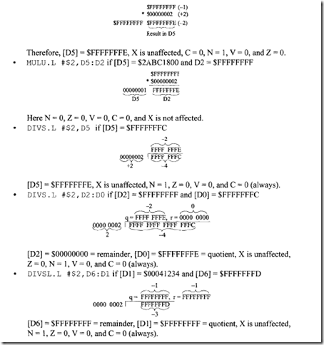
 

80386 Instruction Set

11.3.5 80386 Instruction Set

The 80386 can execute all 16-bit instructions in real and protected modes. This is provided in order to make the 80386 software compatible with the 8086. The 80386 uses either 8- or 32-bit displacements and any register as the base or index register while executing 32-bit code. However, the 80386 uses either 8- or 16-bit displacements with the base and index registers while executing 16-bit code. The base and index registers utilized by the 80386 for 16- and 32-bit addresses are as follows:

image

In the following, the symbol ( ) will indicate the contents of a register or a memory location. A description of some of the new 80386 instructions is given next.

1. Arithmetic Instructions

There are two new sign extension instructions beyond those of the 8086.

CWDE      Sign-extend 16 bit contents of AX to a 32-bit double word in EAX.

CDQ        Sign-extend a double word (32 bits) in EAX to a quadword (64 bits) in EDX:EAX

The 80386 includes all of the 8086 arithmetic instructions plus some new ones. Two of the instructions are as follows:

image

The unsigned multiplication MUL instruction has the same operands as IMUL.

The 80386 divide instructions include all of the 8086 instructions plus some new ones. Some of them are listed next:

image

2. Bit Instructions

image

BSF scans (checks) the 16-bit (word) or 32-bit (double word) number defined by s from right to left (bit 0 to bit 15 or bit 31). The bit number of the first 1 found is stored in d. If the whole 16-bit or 32-bit number is 0, the ZF flag is set to 1; Otherwise, ZF = 0. For example, consider BSF EBX, EDX. If (EDX) = 01241240 16, then after BSF EBX, EDX, (EBX) = 00000006 16 and ZF = 0. The bit number 6 in EDX (contained in the second nibble of EDX) is the first 1 found when (EDX) is scanned from the right.

BSR (bit scan reverse) takes the form

image

BSR scans (checks) the 16-bit or 32-bit number defined by s from the most significant bit (bit 15 or bit 31) to the least significant bit (bit 0). The destination operand d is loaded with the bit index (bit number) of the first set bit. If the bits in the number are all O’s, ZF is set to 1 and operand dis undefined; ZF is reset to 0 if a 1 is found.

BT (bit test) takes the form

image

BT assigns the bit value of operand d (base) specified by operands (bit offset) to the carry flag. Only CF is affected. If operands is an immediate data, only 8 bits are allowed in the instruction. This operand is taken modulo 32 so that the range of immediate bit offset is from 0 to 31. This permits any bit within a register to be selected. If dis a register, the bit value assigned to CF is defined by the value of the bit number defined by s taken modulo the register size (16 or 32). If dis a memory bit string, the desired 16 bits or 32 bits can be determined by adding s (bit index) divided by the operand size (16 or 32) to the memory address of d. The bit within this 16- or 32-bit word is defined by d taken modulo the operand size ( 16 or 32). If d is a memory operand, the 80386 may access 4 bytes in memory starting at effective address plus 4 x [bit offset divided by 32]. As an example, consider BT ex, DX. If (CX) = 081F and (DX) = 0021 16,then after BT ex, DX, because the contents of DX is 3310, the bit number 1 [remainder of33/16 = 1 of CX (value 1)] is reflected in CF and therefore, CF= 1.

BTC (bit test and complement) takes the form

BTC       d,         s

where d and s have the same definitions as for the BT instruction. The bit of d defined by sis reflected in CF. After CF is assigned, the same bit of d defined by sis ones complemented. The 80386 determines the bit number from s (whether s is immediate data or register) and d (whether dis register or memory bit string) in the same way as for the BT instruction.

  • BTR (bit test and reset) takes the form

BTR         d,             s

Where d and s have the same definitions as for the BT instruction. The bit of d defined by s is reflected in CF. After CF is assigned, the same bit of d defined by s is reset to 0. Everything else applicable to the BT instruction also applies to BTR.

  • BTS (bit test and set) takes the form

BTS          d,          s

BTS is the same as BTR except that the specified bit in dis set to 1 after the bit value of d defined by sis reflected in CF. Everything else applicable to the BT instruction also applies to BTS.

3. Set Byte on Condition Instructions

These instructions set a byte to 1 or reset a byte to 0 depending on any of the 16 conditions defined by the status flags. The byte may be located in memory or in a 1-byte general register. These instructions are very useful in implementing Boolean expressions in high-level languages. The general structure of these instructions is SET cc (set byte on condition cc), which sets a byte to 1 if condition cc is true or else resets the byte to 0.

As an example, consider SETB BL (set byte if below; CF = 1). If (BL) = 5216 and CF = I, then, after this instruction is executed, (BL) = 01 16 and eF remains at I ; all other flags (OF, SF, ZF, AF, PF) are undefined. On the other hand, if eF = 0, then, after execution of this instruction, (BL) = 0016, CF = 0, and ZF = 1; all other flags are undefined. The other SET cc instructions can similarly be explained.

4. Conditional Jumps and Loops

JECXZ disp8 jumps if [ECX] = 0; disp8 means a relative address. JECxz tests the contents of the ECX register for zero and not the flags. If [ECX] = 0, then, after execution of the JECXZ instruction, the program branches with a signed 8-bit relative offset(+ 12710 to -128 10 with 0 being positive) defined by disp8. The JECXZ instruction is useful at the beginning of a conditional loop that terminates with a conditional loop instruction such as LOOPNE label. JECXZ prevents entering the loop with [ECX] = 0, which would cause the loop to execute up to 232 times instead of zero times.

The loop instructions are listed next:

image

image

The 80386 loop instructions are similar to those of the 8086 except that if the counter is more than 16 bits, the ECX register is used as the counter.

5. Data Transfer Instructions

a. Move Instructions

The move instructions are described as follows:

imageMOVSX reads the contents of the effective address or register as a byte or a word from the source, sign-extends the value to the operand size of the destination (16 or 32 bits), and stores the result in the destination. No flags are affected. MOVZX, on the other hand, reads the contents of the effective address or register as a byte or a word, zero-extends the value to the operand size of the destination (16 or 32 bits), and stores the result in the destination. No flags are affected. For example, consider MOVSX BX, CL. If (CL) = 8116 and (BX) = 21AF 16, then, after execution of this MOVSX, register BX contains FF81 16 and the contents of CL do not change. Now, consider MOVZX ex, OH. If (CX) = F237 16 and (DH) = 8516, then, after execution of this MOVZX, register CX contains 008516 and DH contents do not change.

b. Push and Pop Instructions

There are new push and pop instructions in the 80386 beyond those of the 8086: PUSHAO and POPAO. PUSHAO saves all 32-bit general registers (the order is EAX, ECX, EDX, EBX, original ESP, EBP, ESI, and EDI) onto the 80386 stack. PUSHAO decrements the stack pointer (ESP) by 3210 to hold the eight 32-bit values. No flags are affected. POPAO reverses a previous PUSHAO. It pops the eight 32-bit registers (the order is EDI, ESI, EBP, ESP, EBX, EDX, ECX, and EAX). The ESP value is discarded instead of loading onto ESP. No flags are affected. Note that ESP is actually popped but thrown away so that (ESP), after popping all the registers, will be incremented by 3210

c. Load Pointer Instructions

There are five instructions in the load pointer instruction category: LOS, LES, LFS, LGS, and LSS. The 80386 can have four versions for each one of these instructions as follows:

image

Note that mem 16:mem 16or mem 16:mem32 defines a memory operand containing the pointers composed of two numbers. The number to the left of the colon corresponds to the pointer’s segment selector; the number to the right corresponds to the offset. These instructions read a full pointer from memory and store it in the selected segment register:specified register. The instruction loads 16 bits into DS (for LOS) or into ES (for LES). The other register loaded is 32 bits for 32-bit operand size and 16 bits for 16-bit operand size. The 16- and 32-bit registers to be loaded are determined by the reg16 or reg32 register specified.

The three instructions LFS, LGS, and LSS are associated with segment registers FS, GS, and SS can similarly be explained.

6. Flag Control Instructions

There are two new flag control instructions in the 80386 beyond those of the 8086: PUSHFD and POPFD. PUSHFD decrements the stack pointer by 4 and saves the 80386 EFLAGS register to the new top of the stack. No flags are affected. POPFD pops the 32 bits (double word) from the top of the stack and stores the value in EFLAGS. All flags except VM and RF are affected.

7. Logical Instructions

There are new logical instructions in the 80386 beyond those of the 8086:

image

For both SHLD and SHRD, the shift count is defined by the low 5 bits, so shifts from 0 to 31 can be obtained.

SHLD shifts the contents of d:s by the specified shift count with the result stored back into d; dis shifted to the left by the shift count with the low-order bits of d filled from the high-order bits of s. The bits ins are not altered after shifting. The carry flag becomes the value of the bit shifted out of the most significant bit of d. If the shift count is zero, this instruction works as an NOP. For the specified shift count, the SF, ZF, and PF flags are set according to the result in d. CF is set to the value of the last bit shifted out. OF and AF are undefined.

SHRD shifts the contents of d:s by the specified shift count to the right with the result stored back into d. The bits in dare shifted right by the shift count, with the high­ order bits filled from the low-order bits of s. The bits ins are not altered after shifting. If the shift count is zero, this instruction operates as an NOP. For the specified shift count, the SF, ZF, and PF flags are set according to the value of the result. CF is set to the value of the last bit shifted out. OF and AF are undefined.

As an example, consider SHLD BX, DX, 2. lf(BX) = 183F16 and (DX) = 0IFI 16, then, after this SHLD, (BX) = 60FC 16, (DX) = 01Fl 16, CF = 0, SF= 0, ZF = 0, and PF = 1. Similarly, the SHRD instruction can be illustrated.

8. String Instructions

a. Compare String Instructions

A new 80386 instruction, CMPS mem32, mem32 (or CMPSD) beyond the compare string instructions available with the 8086 compares 32-bit words ES:EDI (second operand) with DS:ESI and affects the flags. The direction of subtraction of CMPS is (ESI) – (EDI). The left operand (ESI) is the source, and the right operand (EDI) is the destination. This is a reverse of the normal Intel convention in which the left operand is the destination and the right operand is the source. This is true for byte (CMPSB) or word (CMPSW) compare instructions. The result of subtraction is not stored; only the flags are affected. For the first operand (ESI), DS is used as the segment register unless a segment override byte is present; for the second operand (EDI), ES must be used as the segment register and cannot be overridden. ESI and EDI are incremented by 4 if DF = 0 and are decremented by 4 if DF = 1. CMPSD can be preceded by the REPE or REPNE prefix for block comparison. All flags are affected.

b. Load and Move String Instructions

There are new load and move instructions in the 80386 beyond those of 8086. These are LODS mem32 (or LODSD) and MOVS mem32, mem32 (or MOVSD). LODSD loads the (32-bit) double word from a memory location specified by DS: ESI into EAX. After the load, ESI is automatically incremented by 4 if DF = 0 and decremented by 4 if DF = I. No flags are affected. LO DS can be preceded by the REP prefix. LODS is typically used within a loop structure because further processing of the data moved into EAX is normally required. MOVSD copies the (32-bit) double word at the memory location addressed by DS:ESI to the memory location at ES:EDI. DS is used as the segment register for the source and may be overridden. After the move, ESI and EDI are incremented by 4 if DF = 0 and are decremented by 4 if DF = 1. MOVS can be preceded by the REP prefix for block movement of ECX double words. No flags are affected.

c. String I/O Instructions

There are new string I/O instructions in the 80386 beyond those of the 8086: INS mem32, DX (or INSD) and OUTS DX, mem32 {or OUTS D). INSD inputs 32-bit data from a port addressed by the contents of DX into a memory location specified by ES:EDI. ES cannot be overridden. After data transfer, EDI is automatically incremented by 4 if DF = 0 and decremented by 4 if DF = 1. INSD can be preceded by the REP prefix for block input of ECX double words. No flags are affected. OUTSD outputs 32-bit data from a memory location addressed by DS: ESI to a port addressed by the contents of DX. DS can be overridden. After data transfer, ESI is incremented by 4 if DF = 0 and decremented by 4 if DF =

1. OUTS D can be preceded by the REP prefix for block output of ECX double words.

d. Store and Scan String Instructions

There is a new 80386 STOS mem32 (or STOSD) instruction. STOS stores the contents of the EAX register to a double word addressed by ES and EDI. ES cannot be overridden. After the storage, EDI is automatically incremented by

4 if DF = 0 and decremented by 4 if DF = I. No flags are affected. STOS can be preceded by the REP prefix for a block fill of ECX double words. There is also a new scan instruction, the SCAS mem32 (or SCASD) in the 80386. SCASD performs the 32-bit subtraction (EAX) – [memory addressed by ES and EDI]. The result of subtraction is not stored, and the flags are affected. SCASD can be preceded by the REPE or REPNE prefix for block search of ECX double words. All flags are affected.

e. Table Look-Up Translation Instruction

A modified version of the 8086 XLAT instruction is available in the 80386. XLAT mem8 (XLATB) replaces the AL register from the table index to the table entry. AL should be the unsigned index into a table addressed by DS:BX for a 16-bit address and by DS:EBX for the 32-bit address. DS can be overridden. No flags are affected.

9. High-Level Language Instructions

Three instructions, ENTER, LEAVE, and BOUND, are included in the 80386. The ENTER imm16,imm8 instruction creates a stack frame. The data imm8 defines the nesting depth of the subroutine and can be from 0 to 31. The value 0 specifies the first subroutine only. The data imm8 defines the number of stack frame pointers copied into the new stack frame from the preceding frame. After the instruction is executed, the 80386 uses EBP as the current frame pointer and ESP as the current stack pointer. The data imm16 specifies the number of bytes of local variables for which the stack space is to be allocated. If imm8 is zero, ENTER pushes the frame pointer EBP onto the stack; ENTER then subtracts the first operand imm16 from the ESP and sets EBP to the current ESP.
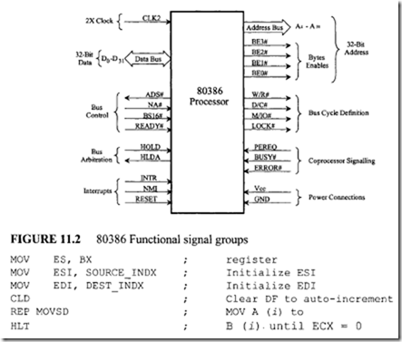
For example, a procedure with 28 bytes of local variables would have an ENTER 2 8 , 0 instruction at its entry point and a LEAVE instruction before every RET. The 28 local bytes would be addressed as offset from EBP. Note that the LEAVE instruction sets ESP TO EBP and then pops EBP. The 80386 uses BP (low 16 bits of EBP) and SP (low 16 bits of ESP) for 16-bit operands and uses EBP and ESP for 32-bit operands.

The BOUND instruction ensures that a signed array index is within the limits specified by a block of memory containing an upper and lower bound. The 80386 provides two forms of the BOUND instruction:

BOUND reg16,              mem32

BOUND reg32,              mem64

The first form is for 16-bit operands. The second form is for 32-bit operands and is included in the 80386 instruction set. For example, consider BOUND EDI, AD DR. Suppose (ADDR) = 32-bit lower bound d1 and (ADDR + 4) = 32 bit upper bound d". If, after execution of this instruction, (EDI) <d1 or>d, the 80386 traps to interrupt 5; otherwise, the array is accessed.

The BOUND instruction is usually placed following the computation of an index value to ensure that the limits of the index value are not violated. This permits a check to determine whether or not an address of an array being accessed is within the array boundaries when the register indirect with index mode is used to access an array element. For example, the following instruction sequence will allow accessing an array with base address in ESI, the index value in EDI, and an array lenght 50 bytes; assuming the 32-bit contents of memory location, 20000100 16 and 20000104 16 are 0 and 49, respectively:

imageExample 11.1

Determine the effect of each of the following 80386 instructions:

(a) CDQ

(b) BTC CX, BX

(c) MOVSX ECX, E7H

Assume (EAX) = FFFFFFFFH, (ECX) = F 1257124H, (EDX) = EEEEEEEEH, and (BX) = 0004H prior to execution of each of these given instructions.

Solution

(a) After CDQ,

(EAX) = FFFFFFFFH

(EDX) = FFFFFFFFH

(b) After BTC ex, BX, bit4 of register CX is reflected in CF and then ones complemented in CX , as is shown below.

image

(c) MOVSX ECX, E7H copies the 8-bit data E7H into the low byte of ECX and then sign­ extends to 32 bits. Therefore, after MOVSX ECX, E7H,

(ECX) = FFFFFFE7H

Example 11.2

Write an 80386 assembly language program to multiply a signed 8-bit number in AL by a signed 32-bit number in ECX. Assume that the segment registers are already initialized. Solution

imageExample 11.3

Write an 80386 assembly language program to move two columns of ten thousand 32-bit numbers from A (i) to B (i). In other words, move A (1) to B (1), A (2) to B (2), and so on.

Solution

image

image