INTRODUCTION TO THE MICROPROCESSOR AND COMPUTER:COMPUTER DATA FORMATS.

COMPUTER DATA FORMATS

Successful programming requires a precise understanding of data formats. In this section, many common computer data formats are described as they are used with the Intel family of micro- processors. Commonly, data appear as ASCII, Unicode, BCD, signed and unsigned integers, and floating-point numbers (real numbers). Other forms are available, but are not presented here because they are not commonly found.

ASCII and Unicode Data

ASCII (American Standard Code for Information Interchange) data represent alphanumeric characters in the memory of a computer system (see Table 1–8). The standard ASCII code is a 7-bit code, with the eighth and most significant bit used to hold parity in some antiquated systems. If ASCII data are used with a printer, the most significant bits are a 0 for alphanumeric printing and 1 for graphics printing. In the personal computer, an extended ASCII character set is selected by placing a 1 in the leftmost bit. Table 1–9 shows the extended ASCII character set, using code 80H–FFH. The extended ASCII characters store some foreign letters and punctuation, Greek

Introduction to the Microprocessor and Computer-0007

characters, mathematical characters, box-drawing characters, and other special characters. Note that extended characters can vary from one printer to another. The list provided is designed to be used with the IBM ProPrinter, which also matches the special character set found with most word processors.

The ASCII control characters, also listed in Table 1–8, perform control functions in a computer system, including clear screen, backspace, line feed, and so on. To enter the control codes through the computer keyboard, hold down the Control key while typing a letter. To obtain the control code 01H, type a Control-A; a 02H is obtained by a Control-B, and so on. Note that the control codes appear on the screen, from the DOS prompt, as ^A for Control-A, ^B for Control-B, and so forth. Also note that the carriage return code (CR) is the Enter key on most modem key- boards. The purpose of CR is to return the cursor or print head to the left margin. Another code that appears in many programs is the line feed code (LF), which moves the cursor down one line.

To use Table 1–8 or 1–9 for converting alphanumeric or control characters into ASCII characters, first locate the alphanumeric code for conversion. Next, find the first digit of the hexadecimal ASCII code. Then find the second digit. For example, the capital letter “A” is ASCII code 41H, and the lowercase letter “a” is ASCII code 61H. Many Windows-based applications, since Windows 95, use the Unicode system to store alphanumeric data. This system stores each character as 16-bit data. The codes 0000H–00FFH are the same as standard ASCII code. The remaining codes, 0100H–FFFFH, are used to store all special characters from many worldwide character sets. This allows software written for the Windows environment to be used in many countries around the world. For complete information on Unicode, visit http://www.unicode.org.

ASCII data are most often stored in memory by using a special directive to the assembler program called define byte(s), or DB. (The assembler is a program that is used to program a computer in its native binary machine language.) An alternative to DB is the word BYTE. The DB and BYTE directives, and several examples of their usage with ASCII-coded character strings, are listed in Example 1–18. Notice how each character string is surrounded by apostrophes (’)—never use the quote (”). Also notice that the assembler lists the ASCII-coded value for each character to the left of the character string. To the far left is the hexadecimal memory location where the character string is first stored in the memory system. For example, the character string WHAT is stored beginning at memory address 001D, and the first letter is stored as 57 (W), followed by 68 (H), and so forth. Example 1–19 shows the same three strings defined as String^ character strings for use with Visual C++ Express 2005 and 2008. Note that Visual C++ uses quotes to surround strings. If an earlier version of C++ is used, then the string is defined with a CString for Microsoft Visual C++ instead of a String^. The ^ symbol indicates that String is a member of the garbage collection heap for managing the storage. A garbage collector cleans off the memory system (frees unused memory) when the object falls from visibility or scope in a C++ program and it also prevents memory leaks.

Introduction to the Microprocessor and Computer-0008

BCD (Binary-Coded Decimal) Data

Binary-coded decimal (BCD) information is stored in either packed or unpacked forms. Packed BCD data are stored as two digits per byte and unpacked BCD data are stored as one digit per byte. The range of a BCD digit extends from 00002 to 10012, or 0–9 decimal. Unpacked BCD data are returned from a keypad or keyboard. Packed BCD data are used for some of the instruc- tions included for BCD addition and subtraction in the instruction set of the microprocessor.

Table 1–10 shows some decimal numbers converted to both the packed and unpacked BCD forms. Applications that require BCD data are point-of-sales terminals and almost any device that performs a minimal amount of simple arithmetic. If a system requires complex arithmetic, BCD data are seldom used because there is no simple and efficient method of performing complex BCD arithmetic.

Introduction to the Microprocessor and Computer-0009

Example 1–20 shows how to use the assembler to define both packed and unpacked BCD data. Example 1–21 shows how to do this using Visual C++ and char or bytes. In all cases, the convention of storing the least-significant data first is followed. This means that to store 83 into memory, the 3 is stored first, and then followed by the 8. Also note that with packed BCD data, the letter H (hexadecimal) follows the number to ensure that the assembler stores the BCD value rather than a decimal value for packed BCD data. Notice how the numbers are stored in memory as unpacked, one digit per byte; or packed, as two digits per byte.

Introduction to the Microprocessor and Computer-0010

Byte-Sized Data

Byte-sized data are stored as unsigned and signed integers. Figure 1–14 illustrates both the unsigned and signed forms of the byte-sized integer. The difference in these forms is the weight of the leftmost bit position. Its value is 128 for the unsigned integer and minus 128 for the signed integer. In the signed integer format, the leftmost bit represents the sign bit of the number, as well as a weight of minus 128. For example, 80H represents a value of 128 as an unsigned number; as a signed number, it represents a value of minus 128. Unsigned integers range in value from 00H to FFH (0–255). Signed integers range in value from -128 to 0 to + 127.

Although negative signed numbers are represented in this way, they are stored in the two’s complement form. The method of evaluating a signed number by using the weights of each bit position is much easier than the act of two’s complementing a number to find its value. This is especially true in the world of calculators designed for programmers.

Introduction to the Microprocessor and Computer-0011

Whenever a number is two’s complemented, its sign changes from negative to positive or positive to negative. For example, the number 00001000 is a +8. Its negative value (-8) is found by two’s complementing the +8. To form a two’s complement, first one’s complement the number. To one’s complement a number, invert each bit of a number from zero to one or from one to zero. Once the one’s complement is formed, the two’s complement is found by adding a one to the one’s complement. Example 1–22 shows how numbers are two’s complemented using this technique.

Introduction to the Microprocessor and Computer-0012

Another, and probably simpler, technique for two’s complementing a number starts with the rightmost digit. Start by writing down the number from right to left. Write the number exactly as it appears until the first one. Write down the first one, and then invert all bits to its left. Example 1–23 shows this technique with the same number as in Example 1–22.

Introduction to the Microprocessor and Computer-0013

To store 8-bit data in memory using the assembler program, use the DB directive as in prior examples or char as in Visual C++ examples. Example 1–24 lists many forms of 8-bit numbers stored in memory using the assembler program. Notice in the example that a hexadecimal number is defined with the letter H following the number, and that a decimal number is written as is, without anything special. Example 1–25 shows the same byte data defined for use with a Visual C++ program. In C/C++ the hexadecimal value is preceded by a 0x to indicate a hexadecimal value.

Introduction to the Microprocessor and Computer-0014

Word-Sized Data

A word (16-bits) is formed with two bytes of data. The least significant byte is always stored in the lowest-numbered memory location, and the most significant byte is stored in the highest. This method of storing a number is called the little endian format. An alternate method, not used with the Intel family of microprocessors, is called the big endian format. In the big endian format, numbers are stored with the lowest location containing the most significant data. The big endian format is used with the Motorola family of microprocessors. Figure 1–15 (a) shows the weights of each bit position in a word of data, and Figure 1–15 (b) shows how the number 1234H appears when stored in the memory locations 3000H and 3001H. The only difference between a signed and an unsigned word in the leftmost bit is position. In the unsigned form, the leftmost bit is unsigned and has a weight of 32,768; in the signed form, its weight is -32,768. As with byte- sized signed data, the signed word is in two’s complement form when representing a negative number. Also, notice that the low-order byte is stored in the lowest-numbered memory location (3000H) and the high-order byte is stored in the highest-numbered location (3001H).

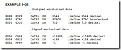
Example 1–26 shows several signed and unsigned word-sized data stored in memory using the assembler program. Example 1–27 shows how to store the same numbers in a Visual C++

Introduction to the Microprocessor and Computer-0015Introduction to the Microprocessor and Computer-0016

program (assuming version 5.0 or newer), which uses the short directive to store a 16-bit integer. Notice that the define word(s) directive, or DW, causes the assembler to store words in the memory instead of bytes, as in prior examples. The WORD directive can also be used to define a word. Notice that the word data is displayed by the assembler in the same form as entered. For example, a l000H is displayed by the assembler as a 1000. This is for our convenience because the number is actually stored in the memory as 00 l0 in two consecutive memory bytes.

Doubleword-Sized Data

Doubleword-sized data requires four bytes of memory because it is a 32-bit number. Doubleword data appear as a product after a multiplication and also as a dividend before a division. In the 80386 through the Core2, memory and registers are also 32 bits in width. Figure 1–16 shows the form used to store doublewords in the memory and the binary weights of each bit position.

When a doubleword is stored in memory, its least significant byte is stored in the lowest numbered memory location, and its most significant byte is stored in the highest-numbered

Introduction to the Microprocessor and Computer-0017

memory location using the little endian format. Recall that this is also true for word-sized data. For example, 12345678H that is stored in memory locations 00100H–00103H is stored with the 78H in memory location 00100H, the 56H in location 00101H, the 34H in location 00102H, and the 12H in location 00103H.

To define doubleword-sized data, use the assembler directive define doubleword(s), or DD. (You can also use the DWORD directive in place of DD.) Example 1–28 shows both signed and unsigned numbers stored in memory using the DD directive. Example 1–29 shows how to define the same doublewords in Visual C++ using the int directive.

Introduction to the Microprocessor and Computer-0018

Integers may also be stored in memory that is of any width. The forms listed here are standard forms, but that doesn’t mean that a 256-byte wide integer can’t be stored in the memory. The microprocessor is flexible enough to allow any size of data in assembly language. When non- standard-width numbers are stored in memory, the DB directive is normally used to store them. For example, the 24-bit number 123456H is stored using a DB 56H, 34H, 12H directive. Note that this conforms to the little endian format. This could also be done in Visual C++ using the char directive.

Real Numbers

Because many high-level languages use the Intel family of microprocessors, real numbers are often encountered. A real number, or a floating-point number, as it is often called, contains two parts: a mantissa, significand, or fraction; and an exponent. Figure 1–17 depicts both the 4- and 8-byte forms of real numbers as they are stored in any Intel system. Note that the 4-byte number is called single-precision and the 8-byte form is called double-precision. The form presented here is the same form specified by the IEEE10 standard, IEEE-754, version 10.0. The standard has been adopted as the standard form of real numbers with virtually all programming languages and many applications packages. The standard also applies the data manipulated by the numeric coprocessor in the personal computer. Figure 1–17 (a) shows the single-precision form that contains a sign-bit, an 8-bit exponent, and a 24-bit fraction (mantissa). Note that because applications often require double-precision floating-point numbers [see Figure 1–17 (b)], the Pentium–Core2 with their 64-bit data bus perform memory transfers at twice the speed of the 80386/80486 microprocessors.

Simple arithmetic indicates that it should take 33 bits to store all three pieces of data. Not true—the 24-bit mantissa contains an implied (hidden) one-bit that allows the mantissa to represent 24 bits while being stored in only 23 bits. The hidden bit is the first bit of the normalized real number. When normalizing a number, it is adjusted so that its value is at least 1, but less than 2.

For example, if 12 is converted to binary (11002), it is normalized and the result is 1.1 * 23. The whole number 1 is not stored in the 23-bit mantissa portion of the number; the 1 is the hidden one-bit. Table 1–11 shows the single-precision form of this number and others.

The exponent is stored as a biased exponent. With the single-precision form of the real number, the bias is 127 (7FH) and with the double-precision form, it is 1023 (3FFH). The bias

Introduction to the Microprocessor and Computer-0019Introduction to the Microprocessor and Computer-0020

and exponent are added before being stored in the exponent portion of the floating-point number. In the previous example, there is an exponent of 23, represented as a biased exponent of 127 + 3 or 130 (82H) in the single-precision form, or as 1026 (402H) in the double-precision form.

There are two exceptions to the rules for floating-point numbers. The number 0.0 is stored as all zeros. The number infinity is stored as all ones in the exponent and all zeros in the mantissa. The sign-bit indicates either a positive or a negative infinity.

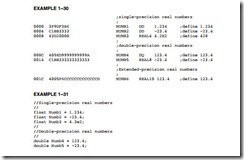
As with other data types, the assembler can be used to define real numbers in both single- and double-precision forms. Because single-precision numbers are 32-bit numbers, use the DD directive or use the define quadword(s), or DQ, directive to define 64-bit double-precision real numbers. Optional directives for real numbers are REAL4, REAL8, and REAL10 for defining single-, double-, and extended precision real numbers. Example 1–30 shows numbers defined in real number format for the assembler. If using the inline assembler in Visual C++ single- precision numbers are defined as float and double-precision numbers are defined as double as shown in Example 1–31. There is no way to define the extended-precision floating-point number for use in Visual C++.

Introduction to the Microprocessor and Computer-0021


QUESTIONS AND PROBLEMS ON INTRODUCTION TO THE MICROPROCESSOR AND COMPUTER.

QUESTIONS AND PROBLEMS

1. Who developed the Analytical Engine?

2. The 1890 census used a new device called a punched card. Who developed the punched card?

3. Who was the founder of IBM Corporation?

4. Who developed the first electronic calculator?

5. The first electronic computer system was developed for what purpose?

6. The first general-purpose, programmable computer was called the .

7. The world’s first microprocessor was developed in 1971 by .

8. Who was the Countess of Lovelace?

9. Who developed the first high-level programming language called FLOWMATIC?

10. What is a von Neumann machine?

11. Which 8-bit microprocessor ushered in the age of the microprocessor?

12. The 8085 microprocessor, introduced in 1977, has sold copies.

13. Which Intel microprocessor was the first to address 1M bytes of memory?

14. The 80286 addresses bytes of memory.

15. How much memory is available to the 80486 microprocessor?

16. When did Intel introduce the Pentium microprocessor?

17. When did Intel introduce the Pentium Pro processor?

18. When did Intel introduce the Pentium 4 microprocessor?

19. Which Intel microprocessor addresses 1T of memory?

20. What is the acronym MIPs?

21. What is the acronym CISC?

22. A binary bit stores a(n) or a(n) .

23. A computer K (pronounced kay) is equal to bytes.

24. A computer M (pronounced meg) is equal to K bytes.

25. A computer G (pronounced gig) is equal to M bytes.

26. A computer P (pronounced peta) is equal to T bytes.

27. How many typewritten pages of information are stored in a 4G-byte memory?

28. The first 1M byte of memory in a DOS-based computer system contains a(n) and a(n) area.

29. How large is the Windows application programming area?

30. How much memory is found in the DOS transient program area?

31. How much memory is found in the Windows systems area?

32. The 8086 microprocessor addresses bytes of memory.

33. The Core2 microprocessor addresses bytes of memory.

34. Which microprocessors address 4G bytes of memory?

35. Memory above the first 1M byte is called memory.

36. What is the system BIOS?

37. What is DOS?

38. What is the difference between an XT and an AT computer system?

39. What is the VESA local bus?

40. The ISA bus holds -bit interface cards.

41. What is the USB?

42. What is the AGP?

43. What is the XMS?

44. What is the SATA interface and where is it used in a system?

45. A driver is stored in the area.

46. The personal computer system addresses bytes of I/O space.

47. What is the purpose of the BIOS?

48. Draw the block diagram of a computer system.

49. What is the purpose of the microprocessor in a microprocessor-based computer?

50. List the three buses found in all computer systems.

51. Which bus transfers the memory address to the I/O device or to the memory?

52. Which control signal causes the memory to perform a read operation?

53. What is the purpose of the IORC signal?

54. If the MRDC signal is a logic 0, which operation is performed by the microprocessor?

55. Define the purpose of the following assembler directives:

(a) DB

(b) DQ

(c) DW

(d) DD

56. Define the purpose of the following 32-bit Visual C++ directives:

(a) char

(b) short

(c) int

(d) float

(e) double

57. Convert the following binary numbers into decimal: (a) 1101.01

(b) 111001.0011

(c) 101011.0101

(d) 111.0001

58. Convert the following octal numbers into decimal: (a) 234.5

(b) 12.3

(c) 7767.07

(d) 123.45

(e) 72.72

59. Convert the following hexadecimal numbers into decimal:

(a) A3.3

(b) 129.C

(c) AC.DC

(d) FAB.3

(e) BB8.0D

60. Convert the following decimal integers into binary, octal, and hexadecimal:

(a) 23

(b) 107

(c) 1238

(d) 92

(e) 173

61. Convert the following decimal numbers into binary, octal, and hexadecimal: (a) 0.625

(b) .00390625

(c) .62890625

(d) 0.75

(e) .9375

62. Convert the following hexadecimal numbers into binary-coded hexadecimal code (BCH):

(a) 23

(b) AD4

(c) 34.AD

(d) BD32

(e) 234.3

63. Convert the following binary-coded hexadecimal numbers into hexadecimal: (a) 1100 0010

(b) 0001 0000 1111 1101

(c) 1011 1100

(d) 0001 0000

(e) 1000 1011 1010

64. Convert the following binary numbers to the one’s complement form: (a) 1000 1000

(b) 0101 1010

(c) 0111 0111

(d) 1000 0000

65. Convert the following binary numbers to the two’s complement form:

(a) 1000 0001

(b) 1010 1100

(c) 1010 1111

(d) 1000 0000

66. Define byte, word, and doubleword.

67. Convert the following words into ASCII-coded character strings:

(a) FROG

(b) Arc

(c) Water

(d) Well

68. What is the ASCII code for the Enter key and what is its purpose?

69. What is the Unicode?

70. Use an assembler directive to store the ASCII-character string ‘What time is it?’ in the memory.

71. Convert the following decimal numbers into 8-bit signed binary numbers:

(a) +32

(b) -12

(c) +100

(d) -92

72. Convert the following decimal numbers into signed binary words:

(a) +1000

(b) -120

(c) +800

(d) -3212

73. Use an assembler directive to store byte-sized -34 into the memory.

74. Create a byte-sized variable called Fred1 and store a -34 in it in Visual C++.

75. Show how the following 16-bit hexadecimal numbers are stored in the memory system (use the standard Intel little endian format):

(a) 1234H

(b) A122H

(c) B100H

76. What is the difference between the big endian and little endian formats for storing numbers that are larger than 8 bits in width?

77. Use an assembler directive to store a 123A hexadecimal into memory.

78. Convert the following decimal numbers into both packed and unpacked BCD forms:

(a) 102

(b) 44

(c) 301

(d) 1000

79. Convert the following binary numbers into signed decimal numbers:

(a) 10000000

(b) 00110011

(c) 10010010

(d) 10001001

80. Convert the following BCD numbers (assume that these are packed numbers) to decimal numbers:

(a) 10001001

(b) 00001001

(c) 00110010

(d) 00000001

81. Convert the following decimal numbers into single-precision floating-point numbers:

(a) +1.5

(b) –10.625

(c) +100.25

(d) –1200

82. Convert the following single-precision floating-point numbers into decimal numbers:

(a) 0 10000000 11000000000000000000000

(b) 1 01111111 00000000000000000000000

(c) 0 10000010 10010000000000000000000

83. Use the Internet to write a short report about any one of the following computer pioneers:

(a) Charles Babbage

(b) Konrad Zuse

(c) Joseph Jacquard

(d) Herman Hollerith

84. Use the Internet to write a short report about any one of the following computer languages:

(a) COBOL

(b) ALGOL

(c) FORTRAN

(d) PASCAL

85. Use the Internet to write a short report detailing the features of the Itanium 2 microprocessor.

86. Use the Internet to detail the Intel 45 nm (nanometer) fabrication technology.


SUMMARY OF INTRODUCTION TO THE MICROPROCESSOR AND COMPUTER.

SUMMARY

1. The mechanical computer age began with the advent of the abacus in 500 B.C. This first mechanical calculator remained unchanged until 1642, when Blaise Pascal improved it. An early mechanical computer system was the Analytical Engine developed by Charles Babbage in 1823. Unfortunately, this machine never functioned because of the inability to create the necessary machine parts.

2. The first electronic calculating machine was developed during World War II by Konrad Zuse, an early pioneer of digital electronics. His computer, the Z3, was used in aircraft and missile design for the German war effort.

3. The first electronic computer, which used vacuum tubes, was placed into operation in 1943 to break secret German military codes. This first electronic computer system, the Colossus, was invented by Alan Turing. Its only problem was that the program was fixed and could not be changed.

4. The first general-purpose, programmable electronic computer system was developed in 1946 at the University of Pennsylvania. This first modern computer was called the ENIAC (Electronics Numerical Integrator and Calculator).

5. The first high-level programming language, called FLOWMATIC, was developed for the UNIVAC I computer by Grace Hopper in the early 1950s. This led to FORTRAN and other early programming languages such as COBOL.

6. The world’s first microprocessor, the Intel 4004, was a 4-bit microprocessor—a programmable controller on a chip—that was meager by today’s standards. It addressed a mere 4096 4-bit memory locations. Its instruction set contained only 45 different instructions.

7. Microprocessors that are common today include the 8086/8088, which were the first 16-bit microprocessors. Following these early 16-bit machines were the 80286, 80386, 80486, Pentium, Pentium Pro, Pentium II, Pentium III, Pentium 4, and Core2 processors. The architecture has changed from 16 bits to 32 bits and, with the Itanium, to 64 bits. With each newer version, improvements followed that increased the processor’s speed and performance. From all indications, this process of speed and performance improvement will continue, although the performance increases may not always come from an increased clock frequency.

8. The DOS-based personal computers contain memory systems that include three main areas: TPA (transient program area), system area, and extended memory. The TPA hold: application programs, the operating system, and drivers. The system area contains memory used for video display cards, disk drives, and the BIOS ROM. The extended memory area is only available to the 80286 through the Core2 microprocessor in an AT-style or ATX-style personal computer system. The Windows-based personal computers contain memory systems that include two main areas: TPA and systems area.

9. The 8086/8088 address 1M byte of memory from locations 00000H–FFFFFH. The 80286 and 80386SX address 16M bytes of memory from locations 000000H–FFFFFFH. The 80386SL addresses 32M bytes of memory from locations 0000000H–1FFFFFFH. The 80386DX through the Core2 address 4G bytes of memory from locations 00000000H–FFFFFFFFH. In addition, the Pentium Pro through the Core2 can operate with a 36-bit address and access up to 64G bytes of memory from locations 000000000H–FFFFFFFFFH. A Pentium 4 or Core2 operating with 64-bit extensions addresses memory from locations 0000000000H– FFFFFFFFFFH for 1T byte of memory.

10. All versions of the 8086 through the Core2 microprocessors address 64K bytes of I/O address space. These I/O ports are numbered from 0000H to FFFFH with I/O ports 0000H–03FFH reserved for use by the personal computer system. The PCI bus allows ports 0400H–FFFFH.

11. The operating system in early personal computers was either MSDOS (Microsoft disk operating system) or PCDOS (personal computer disk operating system from IBM). The operating system performs the task of operating or controlling the computer system, along with its I/O devices. Modern computers use Microsoft Windows in place of DOS as an operating system.

12. The microprocessor is the controlling element in a computer system. The microprocessor performs data transfers, does simple arithmetic and logic operations, and makes simple decisions. The microprocessor executes programs stored in the memory system to perform com- plex operations in short periods of time.

13. All computer systems contain three buses to control memory and I/O. The address bus is used to request a memory location or I/O device. The data bus transfers data between the microprocessor and its memory and I/O spaces. The control bus controls the memory and I/O, and requests reading or writing of data. Control is accomplished with IORC (I/O read control), IOWC (I/O write control), MRDC (memory read control), and MWTC (memory write control).

14. Numbers are converted from any number base to decimal by noting the weights of each position. The weight of the position to the left of the radix point is always the units position in any number system. The position to the left of the units position is always the radix times one. Succeeding positions are determined by multiplying by the radix. The weight of the position to the right of the radix point is always determined by dividing by the radix.

15. Conversion from a whole decimal number to any other base is accomplished by dividing by the radix. Conversion from a fractional decimal number is accomplished by multiplying by the radix.

16. Hexadecimal data are represented in hexadecimal form or in a code called binary-coded hexadecimal (BCH). A binary-coded hexadecimal number is one that is written with a 4-bit binary number that represents each hexadecimal digit.

17. The ASCII code is used to store alphabetic or numeric data. The ASCII code is a 7-bit code; it can have an eighth bit that is used to extend the character set from 128 codes to 256 codes. The carriage return (Enter) code returns the print head or cursor to the left margin. The line feed code moves the cursor or print head down one line. Most modern applications use Unicode, which contains ASCII at codes 0000H–00FFH.

18. Binary-coded decimal (BCD) data are sometimes used in a computer system to store deci- mal data. These data are stored either in packed (two digits per byte) or unpacked (one digit per byte) form.

19. Binary data are stored as a byte (8 bits), word (16 bits), or doubleword (32 bits) in a com- puter system. These data may be unsigned or signed. Signed negative data are always stored in the two’s complement form. Data that are wider than 8 bits are always stored using the little endian format. In 32-bit Visual C++ these data are represented with char (8 bits), short (16 bits) and int (32 bits).

20. Floating-point data are used in computer systems to store whole, mixed, and fractional numbers. A floating-point number is composed of a sign, a mantissa, and an exponent.

21. The assembler directives DB or BYTE define bytes, DW or WORD define words, DD or DWORD define doublewords, and DQ or QWORD define quadwords.


INTRODUCTION TO THE MICROPROCESSOR AND COMPUTER:NUMBER SYSTEMS.

NUMBER SYSTEMS

The use of the microprocessor requires a working knowledge of binary, decimal, and hexadecimal numbering systems. This section of the text provides a background for those who are unfamiliar with these numbering systems. Conversions between decimal and binary, decimal and hexadecimal, and binary and hexadecimal are described.

Digits

Before numbers are converted from one number base to another, the digits of a number system must be understood. Early in our education, we learned that a decimal (base 10) number is constructed with 10 digits: 0 through 9. The first digit in any numbering system is always zero. For example, a base 8 (octal) number contains 8 digits: 0 through 7; a base 2 (binary) number contains 2 digits: 0 and 1. If the base of a number exceeds 10, the additional digits use the letters of the alphabet, beginning with an A. For example, a base 12 number contains 10 digits: 0 through 9, followed by A for 10 and B for 11. Note that a base 10 number does contain a 10 digit, just as a base 8 number does not contain an 8 digit. The most common numbering systems used with computers are decimal, binary, and hexadecimal (base 16). (Many years ago octal numbers were popular.) Each of these number systems are described and used in this section the chapter.

Positional Notation

Once the digits of a number system are understood, larger numbers are constructed by using positional notation. In grade school, we learned that the position to the left of the units position is the tens position, the position to the left of the tens position is the hundreds position, and so forth. (An example is the decimal number 132: This number has 1 hundred, 3 tens, and 2 units.) What probably was not learned was the exponential value of each position: The units position has a weight of 100, or 1; the tens position has weight of 101, or 10; and the hundreds position has a weight of 102, or 100. The exponential powers of the positions are critical for understanding numbers in other numbering systems. The position to the left of the radix (number base) point, called a decimal point only in the decimal system, is always the units position in any number sys- tem. For example, the position to the left of the binary point is always 20, or 1; the position to the left of the octal point is 80, or 1. In any case, any number raised to its zero power is always 1, or the units position.

The position to the left of the units position is always the number base raised to the first power; in a decimal system, this is 101, or 10. In a binary system, it is 21, or 2; and in an octal system, it is 8l, or 8. Therefore, an 11 decimal has a different value from an 11 binary. The decimal number is composed of 1 ten plus 1 unit, and has a value of 11 units; while the binary number 11 is composed of 1 two plus 1 unit, for a value of 3 decimal units. The 11 octal has a value of 9 decimal units.

In the decimal system, positions to the right of the decimal point have negative powers. The first digit to the right of the decimal point has a value of 10-1, or 0.1. In the binary system the first digit to the right of the binary point has a value of 2-1, or 0.5. In general, the principles that apply to decimal numbers also apply to numbers in any other number system.

Example 1–1 shows 110.101 in binary (often written as 110.1012). It also shows the power and weight or value of each digit position. To convert a binary number to decimal, add weights of each digit to form its decimal equivalent. The 110.1012 is equivalent to a 6.625 in decimal (4 + 2 + 0.5 + 0.125). Notice that this is the sum of 22 (or 4) plus 21 (or 2), but 20 (or 1) is not added because there are no digits under this position. The fraction part is com- posed of 2-1 (.5) plus 2-3 (or .125), but there is no digit under the 2-2 (or .25) so .25 is not added.

image

Suppose that the conversion technique is applied to a base 6 number, such as 25.26. Example 1–2 shows this number placed under the powers and weights of each position. In the example, there is a 2 under 61, which has a value of 1210 (2 * 6), and a 5 under 60, which has a value of 5 (5 * 1). The whole number portion has a decimal value of 12 + 5, or 17. The number to the right of the hex point is a 2 under 6-1, which has a value of .333 (2 * .167). The number 25.26, therefore, has a value of 17.333.

Introduction to the Microprocessor and Computer-0000

Conversion to Decimal

The prior examples have shown that to convert from any number base to decimal, determine the weights or values of each position of the number, and then sum the weights to form the decimal equivalent. Suppose that a 125.78 octal is converted to decimal. To accomplish this conversion, first write down the weights of each position of the number. This appears in Example 1–3. The value of 125.78 is 85.875 decimal, or 1 * 64 plus 2 * 8 plus 5 * 1 plus 7 * .125.

Introduction to the Microprocessor and Computer-0001

Notice that the weight of the position to the left of the units position is 8. This is 8 times 1. Then notice that the weight of the next position is 64, or 8 times 8. If another position existed, it would be 64 times 8, or 512. To find the weight of the next higher-order position, multiply the weight of the current position by the number base (or 8, in this example). To calculate the weights of position to the right of the radix point, divide by the number base. In the octal system, the position immediately to the right of the octal point is 1/8, or .125. The next position is .125/8, or .015625, which can also be written as 1/64. Also note that the number in Example 1–3 can also be written as the decimal number 857/8.

Example 1–4 shows the binary number 11011.0111 written with the weights and powers of each position. If these weights are summed, the value of the binary number converted to decimal is 27.4375.

Introduction to the Microprocessor and Computer-0002

It is interesting to note that 2-1 is also 1/2, 2-2 is 1/4, and so forth. It is also interesting to note that 2-4 is 1/16, or .0625. The fractional part of this number is 7/16 or .4375 decimal. Notice that 0111 is a 7 in binary code for the numerator and the rightmost one is in the 1/16 position for the denominator. Other examples: The binary fraction of .101 is 5/8 and the binary fraction of .001101 is 13/64.

Hexadecimal numbers are often used with computers. A 6A.CH (H for hexadecimal) is illustrated with its weights in Example 1–5. The sum of its digits is 106.75, or 1063⁄4. The whole number part is represented with 6 * 16 plus 10 1A2 * 1. The fraction part is 12 (C) as a numerator and 16 (16-1) as the denominator, or 12/16, which is reduced to 3/4.

Introduction to the Microprocessor and Computer-0003

Conversion from Decimal

Conversions from decimal to other number systems are more difficult to accomplish than con- version to decimal. To convert the whole number portion of a number to decimal, divide by 1 radix. To convert the fractional portion, multiply by the radix.

Whole Number Conversion from Decimal. To convert a decimal whole number to another number system, divide by the radix and save the remainders as significant digits of the result. An algorithm for this conversion as is follows:

1. Divide the decimal number by the radix (number base).

2. Save the remainder (first remainder is the least significant digit).

3. Repeat steps 1 and 2 until the quotient is zero.

For example, to convert a 10 decimal to binary, divide it by 2. The result is 5, with a remain- der of 0. The first remainder is the units position of the result (in this example, a 0). Next divide the 5 by 2. The result is 2, with a remainder of 1. The 1 is the value of the twos (21) position. Continue the division until the quotient is a zero. Example 1–6 shows this conversion process. The result is written as 10102 from the bottom to the top.

Introduction to the Microprocessor and Computer-0004

Converting from a Decimal Fraction. Conversion from a decimal fraction to another number base is accomplished with multiplication by the radix. For example, to convert a decimal fraction into binary, multiply by 2. After the multiplication, the whole number portion of the result is saved as a significant digit of the result, and the fractional remainder is again multiplied by the radix. When the fraction remainder is zero, multiplication ends. Note that some numbers are never-ending (repetend). That is, a zero is never a remainder. An algorithm for conversion from a decimal fraction is as follows:

1. Multiply the decimal fraction by the radix (number base).

2. Save the whole number portion of the result (even if zero) as a digit. Note that the first result is written immediately to the right of the radix point.

3. Repeat steps 1 and 2, using the fractional part of step 2 until the fractional part of step 2 is zero.

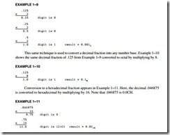
Suppose that a .125 decimal is converted to binary. This is accomplished with multiplications by 2, as illustrated in Example 1–9. Notice that the multiplication continues until the fractional remainder is zero. The whole number portions are written as the binary fraction (0.001) in this example.

Introduction to the Microprocessor and Computer-0005

Binary-Coded Hexadecimal

Binary-coded hexadecimal (BCH) is used to represent hexadecimal data in binary code. A binary-coded hexadecimal number is a hexadecimal number written so that each digit is repre- sented by a 4-bit binary number. The values for the BCH digits appear in Table 1–7.

Hexadecimal numbers are represented in BCH code by converting each digit to BCH code with a space between each coded digit. Example 1–12 shows a 2AC converted to BCH code. Note that each BCH digit is separated by a space.

Introduction to the Microprocessor and Computer-0006

The purpose of BCH code is to allow a binary version of a hexadecimal number to be written in a form that can easily be converted between BCH and hexadecimal. Example 1–13 shows a BCH coded number converted back to hexadecimal code.

EXAMPLE 1–13

1000 0011 1101 . 1110 = 83D.E

Complements

At times, data are stored in complement form to represent negative numbers. There are two systems that are used to represent negative data: radix and radix 1 complements. The earliest system was the radix -1 complement, in which each digit of the number is subtracted from the radix -1 to gen- erate the radix -1 complement to represent a negative number.

Example 1–14 shows how the 8-bit binary number 01001100 is one’s (radix -1) comple- mented to represent it as a negative value. Notice that each digit of the number is subtracted from one to generate the radix -1 (one’s) complement. In this example, the negative of 01001100 is 10110011. The same technique can be applied to any number system, as illustrated in Example 1–15, in which the fifteen’s (radix -1) complement of a 5CD hexadecimal is com- puted by subtracting each digit from a fifteen.

image

Today, the radix -1 complement is not used by itself; it is used as a step for finding the radix complement. The radix complement is used to represent negative numbers in modem computer systems. (The radix -1 complement was used in the early days of computer technology.) The main problem with the radix -1 complement is that a negative or a positive zero exists; in the radix complement system, only a positive zero can exist.

To form the radix complement, first find the radix -1 complement, and then add a one to the result. Example 1–16 shows how the number 0100 1000 is converted to a negative value by two’s (radix) complementing it.

image

To prove that a 0100 1000 is the inverse (negative) of a 1011 1000, add the two together to form an 8-digit result. The ninth digit is dropped and the result is zero because a 0100 1000 is a positive 72, while a 1011 1000 is a negative 72. The same technique applies to any number system. Example 1–17 shows how the inverse of a 345 hexadecimal is found by first fifteen’s complement- ing the number, and then by adding one to the result to form the sixteen’s complement. As before, if the original 3-digit number 345 is added to the inverse of CBB, the result is a 3-digit 000. As before, the fourth bit (carry) is dropped. This proves that 345 is the inverse of CBB. Additional information about one’s and two’s complements is presented with signed numbers in the next section of the text.

image


INTRODUCTION TO THE MICROPROCESSOR AND COMPUTER:The Microprocessor-Based Personal Computer System

1–2                           THE MICROPROCESSOR-BASED PERSONAL COMPUTER SYSTEM


Computer systems have undergone many changes recently. Machines that once filled large areas have been reduced to small desktop computer systems because of the microprocessor. Although these desktop computers are compact, they possess computing power that was only dreamed of a few years ago. Million-dollar mainframe computer systems, developed in the early 1980s, are not as powerful as the Pentium Core2-based computers of today. In fact, many smaller compa- nies have replaced their mainframe computers with microprocessor-based systems. Companies such as DEC (Digital Equipment Corporation, now owned by Hewlett-Packard Company) have stopped producing mainframe computer systems in order to concentrate their resources on microprocessor-based computer systems.

This section shows the structure of the microprocessor-based personal computer system. This structure includes information about the memory and operating system used in many microprocessor-based computer systems.

See Figure 1–6 for the block diagram of the personal computer. This diagram also applies to any computer system, from the early mainframe computers to the latest microprocessor-based systems. The block diagram is composed of three blocks that are interconnected by buses. (A bus is the set of common connections that carry the same type of information. For example, the address bus, which contains 20 or more connections, conveys the memory address to the mem- ory.) These blocks and their function in a personal computer are outlined in this section of the text.


The Memory and I/O System


The memory structure of all Intel-based personal computers is similar. This includes the first per- sonal computers based upon the 8088, introduced in 1981 by IBM, to the most powerful high- speed versions of today, based on the Pentium 4 or Core2. Figure 1–7 illustrates the memory map of a personal computer system. This map applies to any IBM personal computer or to any of the many IBM-compatible clones that are in existence.

The memory system is divided into three main parts: TPA (transient program area), system area, and XMS (extended memory system). The type of microprocessor in your computer deter- mines whether an extended memory system exists. If the computer is based upon a really old 8086 or 8088 (a PC or XT), the TPA and systems area exist, but there is no extended memory


clip_image001[4]Buses


clip_image002[4]clip_image003[4]clip_image004[3]clip_image005[3]clip_image006[3]clip_image007[3]Memory system                                        Microprocessor                                         I/O system


Dynamic RAM (DRAM) Static RAM (SRAM) Cache

Read-only (ROM) Flash memory EEPROM SDRAM RAMBUS

DDR DRAM


8086

8088

80186

80188

80286

80386

80486

Pentium Pentium Pro Pentium II Pentium III Pentium 4 Core2


Printer

Serial communications Floppy disk drive

Hard disk drive Mouse

CD-ROM drive Plotter Keyboard Monitor

Tape backup Scanner DVD


FIGURE 1–6    The block diagram of a microprocessor-based computer system.


area. The PC and XT computers contain 640K bytes of TPA and 384K bytes of system memory, for a total memory size of 1M bytes. We often call the first 1M byte of memory the real or con- ventional memory system because each Intel microprocessor is designed to function in this area by using its real mode of operation.

Computer systems based on the 80286 through the Core2 not only contain the TPA (640K bytes) and system area (384K bytes), they also contain extended memory. These machines are


clip_image008[3]FIGURE 1–7    The memory map of a personal computer.


Extended memory


15M bytes in the 80286 or 80386SX 31M bytes in the 80386SL/SLC 63M bytes in the 80386EX


System area 384K bytes


TPA

640K bytes


4095M bytes in the 80386DX, 80486, and Pentium 64G bytes in the Pentium Pro, Pentium II, Pentium III, Pentium 4, and Core2


1M bytes of real (conventional) memory


often called AT class machines. The PS/l and PS/2, produced by IBM, are other versions of the same basic memory design. Sometimes, these machines are also referred to as ISA (industry standard architecture) or EISA (extended ISA) machines. The PS/2 is referred to as a micro- channel architecture system, or ISA system, depending on the model number.

A change beginning with the introduction of the Pentium microprocessor and the ATX class machine is the addition of a bus called the PCI (peripheral component interconnect) bus, now being used in all Pentium through Core2 systems. Extended memory contains up to 15M bytes in the 80286 and 80386SX-based computers, and up to 4095M bytes in the 80386DX, 80486, and Pentium microprocessors, in addition to the first 1M byte of real or conventional memory. The Pentium Pro through Core2 computer systems have up to 1M less than 4G or 1 M less than 64G of extended memory. Servers tend to use the larger 64G memory map, while home/business computers use the 4G-byte memory map. The ISA machine contains an 8-bit peripheral bus that is used to interface 8-bit devices to the computer in the 8086/8088-based PC or XT computer system. The AT class machine, also called an ISA machine, uses a l6-bit peripheral bus for interface and may contain the 80286 or above microprocessor. The EISA bus is a 32-bit peripheral interface bus found in a few older 80386DX- and 80486-based systems. Note that each of these buses is compatible with the earlier versions. That is, the 8-bit interface card functions in the 8-bit ISA, l6-bit ISA, or 32-bit EISA bus system. Likewise, a l6-bit inter- face card functions in the l6-bit ISA or 32-bit EISA system.

Another bus type found in many 80486-based personal computers is called the VESA local bus, or VL bus. The local bus interfaces disk and video to the microprocessor at the local bus level, which allows 32-bit interfaces to function at the same clocking speed as the microproces- sor. A recent modification to the VESA local bus supports the 64-bit data bus of the Pentium microprocessor and competes directly with the PCI bus, although it has generated little, if any, interest. The ISA and EISA standards function at only 8 MHz, which reduces the performance of the disk and video interfaces using these standards. The PCI bus is either a 32- or 64-bit bus that is specifically designed to function with the Pentium through Core2 microprocessors at a bus speed of 33 MHz.

Three newer buses have appeared in ATX class systems. The first to appear was the USB (universal serial bus). The universal serial bus is intended to connect peripheral devices such as keyboards, a mouse, modems, and sound cards to the microprocessor through a serial data path and a twisted pair of wires. The main idea is to reduce system cost by reducing the number of wires. Another advantage is that the sound system can have a separate power supply from the PC, which means much less noise. The data transfer rates through the USB are 10 Mbps at pre- sent for USB1; they increase to 480 Mbps in USB2.

The second newer bus is the AGP (advanced graphics port) for video cards. The advanced graphics port transfers data between the video card and the microprocessor at higher speeds (66 MHz, with a 64-bit data path, or 533M bytes per second) than were possible through any other bus or connection. The latest AGP speed is 8X or 2G bytes per second. This video sub- system change has been made to accommodate the new DVD players for the PC.

The latest new buses to appear are the serial ATA interface (SATA) for hard disk drives and the PCI Express bus for the video card. The SATA bus transfers data from the PC to the hard disk drive at rates of 150M bytes per second or 300M bytes for SATA-2. The serial ATA standard will eventually reach speeds of 450M bytes per second. Today PCI Express bus video cards operate at 16X speeds.


The TPA. The transient program area (TPA) holds the DOS (disk operating system) operating system and other programs that control the computer system. The TPA is a DOS con- cept and not really applicable in Windows. The TPA also stores any currently active or inactive DOS application programs. The length of the TPA is 640K bytes. As mentioned, this area of memory holds the DOS operating system, which requires a portion of the TPA to function.


FIGURE 1–8    The memory map of the TPA in a personal computer. (Note that this map will vary between systems.)


MSDOS program


Free TPA


9FFFF


9FFF0


COMMAND.COM


Device drivers such as MOUSE.SYS


MSDOS program


IO.SYS program


               BIOS communications area


Interrupt vectors


08E30


08490


02530


01160


00700


00500


00400


00000


In practice, the amount of memory remaining for application software is about 628K bytes if MSDOS9 version 7.x is used as an operating system. Earlier versions of DOS required more of the TPA area and often left only 530K bytes or less for application programs. Figure 1–8 shows the organization of the TPA in a computer system running DOS.

The DOS memory map shows how the many areas of the TPA are used for system pro- grams, data, and drivers. It also shows a large area of memory available for application pro- grams. To the left of each area is a hexadecimal number that represents the memory addresses that begin and end each data area. Hexadecimal memory addresses or memory locations are used to number each byte of the memory system. (A hexadecimal number is a number repre- sented in radix 16 or base 16, with each digit representing a value from 0 to 9 and A to F. We often end a hexadecimal number with an H to indicate that it is a hexadecimal value. For exam- ple, 1234H is 1234 hexadecimal. We also represent hexadecimal data as 0xl234 for a 1234 hexadecimal.)


clip_image009[3]9MSDOS is a trademark of Microsoft Corporation and version 7.x is supplied with Windows XP.


The Interrupt vectors access various features of the DOS, BIOS (basic I/O system), and applications. The system BIOS is a collection of programs stored in either a read-only (ROM) or flash memory that operates many of the I/O devices connected to your computer system. The system BIOS and DOS communications areas contain transient data used by programs to access I/O devices and the internal features of the computer system. These are stored in the TPA so they can be changed as the DOS operates.

The IO.SYS is a program that loads into the TPA from the disk whenever an MSDOS sys- tem is started. The IO.SYS contains programs that allow DOS to use the keyboard, video display, printer, and other I/O devices often found in the computer system. The IO.SYS program links DOS to the programs stored on the system BIOS ROM.

The size of the driver area and number of drivers changes from one computer to another. Drivers are programs that control installable I/O devices such as a mouse, disk cache, hand scan- ner, CD-ROM memory (Compact Disk Read-Only Memory), DVD (Digital Versatile Disk), or installable devices, as well as programs. Installable drivers are programs that control or drive devices or programs that are added to the computer system. DOS drivers are normally files that have an extension of .SYS, such as MOUSE.SYS; in DOS version 3.2 and later, the files have an extension of .EXE, such as EMM386.EXE. Note that even though these files are not used by Windows, they are still used to execute DOS applications, even with Windows XP. Windows uses a file called SYSTEM.INI to load drivers used by Windows. In newer versions of Windows such as Windows XP, a registry is added to contain information about the system and the drivers used by the system. You can view the registry with the REGEDIT program.

The COMMAND.COM program (command processor) controls the operation of the computer from the keyboard when operated in the DOS mode. The COMMAND.COM program processes the DOS commands as they are typed from the keyboard. For example, if DIR is typed, the COMMAND.COM program displays a directory of the disk files in the current disk direc- tory. If the COMMAND.COM program is erased, the computer cannot be used from the key- board in DOS mode. Never erase COMMAND.COM, IO.SYS, or MSDOS.SYS to make room for other software, or your computer will not function.


The System Area. The DOS system area, although smaller than the TPA, is just as important. The system area contains programs on either a read-only memory (ROM) or flash memory, and areas of read/write (RAM) memory for data storage. Figure 1–9 shows the system area of a typical personal computer system. As with the map of the TPA, this map also includes the hexa- decimal memory addresses of the various areas.

The first area of the system space contains video display RAM and video control programs on ROM or flash memory. This area starts at location A0000H and extends to location C7FFFH. The size and amount of memory used depends on the type of video display adapter attached to the system. Display adapters generally have their video RAM located at A0000H–AFFFFH, which stores graphical or bit-mapped data, and the memory at B0000H–BFFFFH stores text data. The video BIOS, located on a ROM or flash memory, is at locations C0000H–C7FFFH and contains programs that control the DOS video display.

The area at locations C8000H–DFFFFH is often open or free. This area is used for the expanded memory system (EMS) in a PC or XT system, or for the upper memory system in an AT system. Its use depends on the system and its configuration. The expanded memory system allows a 64K-byte page frame of memory to be used by application programs. This 64K-byte page frame (usually locations D0000H through DFFFFH) is used to expand the memory system by switching in pages of memory from the EMS into this range of memory addresses.

Memory locations E0000H–EFFFFH contain the cassette BASIC language on ROM found in early IBM personal computer systems. This area is often open or free in newer computer systems.

Finally, the system BIOS ROM is located in the top 64K bytes of the system area (F0000H–FFFFFH). This ROM controls the operation of the basic I/O devices connected to the


FIGURE 1–9    The system area of a typical personal computer.


FFFFF


BIOS system ROM


F0000                                                                     


BASIC language ROM (only on early PCs)

E0000                                                                      


Free area


C8000


Hard disk controller ROM

                   LAN controller ROM             


Video BIOS ROM

C0000                                                                      


Video RAM (text area)


B0000                                                                     


Video RAM (graphics area)


A0000


clip_image010[3]computer system. It does not control the operation of the video system, which has its own BIOS ROM at location C0000H. The first part of the system BIOS (F0000H–F7FFFH) often contains programs that set up the computer; the second part contains procedures that control the basic I/O system.


Windows Systems. Modern computers use a different memory map with Windows than the DOS memory maps of Figures 1–8 and 1–9. The Windows memory map appears in Figure 1–10 and has two main areas, a TPA and a system area. The difference between it and the DOS memory map are the sizes and locations of these areas.

The Windows TPA is the first 2G bytes of the memory system from locations 00000000H to 7FFFFFFFH. The Windows system area is the last 2G bytes of memory from locations 80000000H to FFFFFFFFH. It appears that the same idea used to construct the DOS memory map was also used in a modern Windows-based system. The system area is where the system BIOS is located and also the video memory. Also located in the system area is the actual Windows program and drivers. Every program that is written for Windows can use up to 2G bytes of memory located at linear addresses 00000000H through 7FFFFFFFH. This is even true in a 64-bit system, which does allow access to more memory, but not as a direct part of Windows. Information that is larger than 2G must be swapped into the Windows TPA area from another area of memory. In future versions of Windows and the Pentium, this will most likely be changed. The current version of Windows 64 (which is now a part of Windows Vista) supports up to 8G bytes of Windows memory.


clip_image012[3]FIGURE 1–10    The memory map used by Windows XP.


Does this mean that any program written for Windows will begin at physical address 00000000H? No, the memory system physical map is much different for the linear programming model shown in Figure 1–10. Every process in a Windows Vista, Windows XP, or Windows 2000 system has its own set of page tables, which define where in the physical memory each 4K-byte page of the process is located. This means that the process can be located anywhere in the mem- ory, even in noncontiguous pages. Page tables and the paging structure of the microprocessor are discussed later in this chapter and are beyond the scope of the text at this point. As far as an application is concerned, you will always have 2G bytes of memory even if the computer has less memory. The operating system (Windows) handles assigning physical memory to the application and if not enough physical memory exists, it uses the hard disk drive for any that is not available.


I/O Space. The I/O (input/output) space in a computer system extends from I/O port 0000H to port FFFFH. (An I/O port address is similar to a memory address, except that instead of addressing memory, it addresses an I/O device.) The I/O devices allow the microprocessor to communicate between itself and the outside world. The I/O space allows the computer to access up to 64K different 8-bit I/O devices, 32K different 16-bit devices, or 16K different 32-bit devices. The 64-bit extensions support the same I/O space and I/O sizes as the 32-bit version and does not add 64-bit I/O devices to the system. A great number of these locations are available for expansion in most computer systems. Figure 1–11 shows the I/O map found in many personal computer systems. To view the map on your computer in Windows, go to the Control Panel, Performance and Maintenance, System, Hardware tab, Device Manager, View tab, then select resources by type and click on the plus next to Input/Output (I/O).


FIGURE 1–11    Some

I/O locations in a typical personal computer.


clip_image014[3]


The I/O area contains two major sections. The area below I/O location 0400H is consid- ered reserved for system devices; many are depicted in Figure 1–11. The remaining area is available I/O space for expansion that extends from I/O port 0400H through FFFFH. Generally, I/O addresses between 0000H and 00FFH address components on the main board of the com- puter, while addresses between 0100H and 03FFH address devices located on plug-in cards (or on the main board). Note that the limitation of I/O addresses between 0000 and 03FFH comes from the original PC standard, as specified by IBM. When using the ISA bus, you must only use addresses between 0000H and 03FFH. The PCI bus uses I/O address between 0400H and FFFFH.

Various I/O devices that control the operation of the system are usually not directly addressed. Instead, the system BIOS ROM addresses these basic devices, which can vary slightly in location and function from one computer to the next. Access to most I/O devices should always be made


through Windows, DOS, or BIOS function calls to maintain compatibility from one computer system to another. The map shown in Figure 1–11 is provided as a guide to illustrate the I/O space in the system.


The Microprocessor


At the heart of the microprocessor-based computer system is the microprocessor integrated circuit. The microprocessor, sometimes referred to as the CPU (central processing unit), is the controlling element in a computer system. The microprocessor controls memory and I/O through a series of connections called buses. The buses select an I/O or memory device, transfer data between an I/O device or memory and the microprocessor, and control the I/O and memory system. Memory and I/O are controlled through instructions that are stored in the memory and executed by the microprocessor.

The microprocessor performs three main tasks for the computer system: (1) data transfer between itself and the memory or I/O systems, (2) simple arithmetic and logic operations, and

(3) program flow via simple decisions. Although these are simple tasks, it is through them that the microprocessor performs virtually any series of operations or tasks.

The power of the microprocessor is in its capability to execute billions of millions of instructions per second from a program or software (group of instructions) stored in the mem- ory system. This stored program concept has made the microprocessor and computer system very powerful devices. (Recall that Babbage also wanted to use the stored program concept in his Analytical Engine.)

Table 1–4 shows the arithmetic and logic operations executed by the Intel family of micro- processors. These operations are very basic, but through them, very complex problems are solved. Data are operated upon from the memory system or internal registers. Data widths are variable and include a byte (8 bits), word (16 bits), and doubleword (32 bits). Note that only the 80386 through the Core2 directly manipulate 8-, 16-, and 32-bit numbers. The earlier 8086–80286 directly manipulated 8 and 16-bit numbers, but not 32-bit numbers. Beginning with the 80486, the microprocessor contained a numeric coprocessor that allowed it to perform complex arith- metic using floating-point arithmetic. The numeric coprocessor, which is similar to a calculator chip, was an additional component in the 8086 through the 80386-based personal computer. The numeric coprocessor is also capable of performing integer operations on quadwords (64 bits). The MMX and SIMD units inside the Pentium through Core2 function with integers and floating- point number in parallel. The SIMD unit requires numbers stored as octalwords (128 bits).

Another feature that makes the microprocessor powerful is its ability to make simple decisions based upon numerical facts. For example, a microprocessor can decide if a number is zero, if it is positive, and so forth. These simple decisions allow the microprocessor to modify the


TABLE 1–4     Simple arithmetic and logic operations.


clip_image015[3]Operation                             Comment


clip_image016[3]Addition Subtraction Multiplication Division

AND                            Logical multiplication

OR                               Logic addition

NOT                            Logical inversion

NEG                            Arithmetic inversion Shift

clip_image017[3]Rotate


TABLE 1–5    Decisions found in the 8086 through Core2 microprocessors.


clip_image018[5]Decision                                              Comment


clip_image019[3]Zero                  Test a number for zero or not-zero

Sign                  Test a number for positive or negative

Carry                 Test for a carry after addition or a borrow after subtraction

Parity                 Test a number for an even or an odd number of ones

clip_image018[6]Overflow          Test for an overflow that indicates an invalid result after a signed addition or a signed subtraction


program flow, so that programs appear to think through these simple decisions. Table 1–5 lists the decision-making capabilities of the Intel family of microprocessors.


Buses. A bus is a common group of wires that interconnect components in a computer system. The buses that interconnect the sections of a computer system transfer address, data, and control information between the microprocessor and its memory and I/O systems. In the microprocessor– based computer system, three buses exist for this transfer of information: address, data, and con- trol. Figure 1–12 shows how these buses interconnect various system components such as the microprocessor, read/write memory (RAM), read-only memory (ROM or flash), and a few I/O devices.

The address bus requests a memory location from the memory or an I/O location from the I/O devices. If I/O is addressed, the address bus contains a 16-bit I/O address from 0000H through FFFFH. The 16-bit I/O address, or port number, selects one of 64K different I/O devices. If memory is addressed, the address bus contains a memory address, which varies in width with the different versions of the microprocessor. The 8086 and 8088 address 1M byte of memory, using a 20-bit address that selects locations 00000H–FFFFFH. The 80286 and 80386SX address 16M bytes of memory using a 24-bit address that selects locations 000000H–FFFFFFH. The 80386SL, 80386SLC, and 80386EX address 32M bytes of memory, using 25-bit address that selects locations 0000000H–1FFFFFFH. The 80386DX, 80486SX, and 80486DX address


Address bus


μp                                             Data bus


MWTC MRDC IOWC IORC


Read-only memory ROM


Read/write memory RAM


Keyboard


Printer


clip_image020[3]FIGURE 1–12    The block diagram of a computer system showing the address, data, and control bus structure.


clip_image021[3]TABLE 1–6     The Intel family of microprocessor bus and memory sizes.


Microprocessor                                              Data Bus Width     Address Bus Width     Memory Size


clip_image022[3]8086                                                                              16                              20                             1M

8088                                                                                8                              20                             1M

80186                                                                           16                              20                             1M

80188                                                                              8                              20                             1M

80286                                                                           16                              24                           16M

80386SX                                                                      16                              24                           16M

80386DX                                                                      32                              32                             4G

80386EX                                                                      16                              26                           64M

80486                                                                           32                              32                             4G

Pentium                                                                        64                              32                             4G

Pentium Pro–Core2                                                   64                              32                             4G


Pentium Pro–Core2

(if extended addressing is enabled)

Pentium 4 and Core2

with 64-bit extensions enabled


64                             36                           64G


64                             40                              1T


clip_image023[3]Itanium                                                                       128                              40                              1T


4G bytes of memory, using a 32-bit address that selects locations 00000000H–FFFFFFFFH. The Pentium also addresses 4G bytes of memory, but it uses a 64-bit data bus to access up to 8 bytes of memory at a time. The Pentium Pro through Core2 microprocessors have a 64-bit data bus and a 32-bit address bus that address 4G of memory from location 00000000H–FFFFFFFFH, or a 36-bit address bus that addresses 64G of memory at locations 000000000H–FFFFFFFFFH, depending on their configuration. Refer to Table 1–6 for complete listing of bus and memory sizes of the Intel family of microprocessors.

The 64-bit extensions to the Pentium family provide 40 address pins in its current version that allow up to 1T byte of memory to be accessed through its 10 digit hexadecimal address. Note that 240 is 1 terra. In future editions of the 64-bit microprocessors Intel plans to expand the number of address bits to 52, and ultimately to 64 bits. A 52-bit address bus allows 4P (Peta) bytes of memory to be accessed and a 64-bit address bus allows 16E (Exa) bytes of memory.

The data bus transfers information between the microprocessor and its memory and I/O address space. Data transfers vary in size, from 8 bits wide to 64 bits wide in various members of the Intel microprocessor family. For example, the 8088 has an 8-bit data bus that transfers 8 bits of data at a time. The 8086, 80286, 80386SL, 80386SX, and 80386EX transfer 16 bits of data through their data buses; the 80386DX, 80486SX, and 80486DX transfer 32 bits of data; and the Pentium through Core2 microprocessors transfer 64 bits of data. The advantage of a wider data bus is speed in applications that use wide data. For example, if a 32-bit number is stored in mem- ory, it takes the 8088 microprocessor four transfer operations to complete because its data bus is only 8 bits wide. The 80486 accomplishes the same task with one transfer because its data bus is 32 bits wide. Figure 1–13 shows the memory widths and sizes of the 8086–80486 and Pentium through Core2 microprocessors. Notice how the memory sizes and organizations differ between various members of the Intel microprocessor family. In all family members, the mem- ory is numbered by byte. Notice that the Pentium through Core2 microprocessors all contain a 64-bit-wide data bus.

clip_image024[5]clip_image025[3]clip_image026[3]clip_image027[3]The control bus contains lines that select the memory or I/O and cause them to perform a read or write operation. In most computer systems, there are four control bus connections: MRDC (memory read control), MWTC (memory write control), IORC (I/O read control), and IOWC (I/O write control). Note that the overbar indicates that the control signal is active-low; that is,


clip_image024[6]it is active when a logic zero appears on the control line. For example, if IOWC = 0, the microprocessor is writing data from the data bus to an I/O device whose address appears on the address bus. Note that these control signal names are slightly different in various versions of the microprocessor.

clip_image028[3]The microprocessor reads the contents of a memory location by sending the memory an address through the address bus. Next, it sends the memory read control signal (MRDC) to cause the memory to read data. Finally, the data read from the memory are passed to the microproces- sor through the data bus. Whenever a memory write, I/O write, or I/O read occurs, the same sequence ensues, except that different control signals are issued and the data flow out of the microprocessor through its data bus for a write operation.


clip_image029[9]clip_image030[13]clip_image031[5]clip_image032[5]clip_image033[9]


8 bits


1M byte


FFFFF FFFFE FFFFD


FFFFFF FFFFFD FFFFFB


High bank (Odd bank)


clip_image034[3]


8 bits


8M bytes


FFFFFE FFFFFC FFFFFA


Low bank (Even bank)


00002

00001

00000


D7–D0

8088 microprocessor


000005

000003

000001


D15–D8


000004

000002

000000


8 bits


8M bytes


D7–D0


8086 microprocessor (memory is only 1M bytes)

80286 microprocessor 80386SX microprocessor

80386SL microprocessor (memory is 32M bytes) 80386SLC microprocessor (memory is 32M bytes)


FFFFFFFF FFFFFFFB FFFFFFF7


0000000B

00000007

00000003


Bank 3


clip_image029[10]clip_image030[14]


8 bits


1G byte


D31–D24


FFFFFFFE FFFFFFFA FFFFFFF6


0000000A

00000006

00000002


Bank 2


clip_image035[9]clip_image036[3]


8 bits


1G byte


D23–D16


FFFFFFFD FFFFFFF9 FFFFFFF5


00000009

00000005

00000001


80386DX microprocessor 80486SX microprocessor 80486DX microprocessor


Bank 1


clip_image035[10]clip_image037[3]


8 bits


1G byte


D15–D8


FFFFFFFC FFFFFFF8 FFFFFFF4


00000008

00000004

00000000


Bank 0


clip_image032[6]clip_image033[10]


8 bits


1G byte


D7–D0


FIGURE 1–13    The physical memory systems of the 8086 through the Core2 microprocessors.


FFFFFFFF FFFFFFF7 FFFFFFEF


00000017

0000000F

00000007


Bank 7


clip_image035[11]clip_image038[5]


8 bits


512M bytes


D63–D56


FFFFFFFE FFFFFFF6 FFFFFFEE


00000016

0000000E

00000006


Bank 6


clip_image029[11]clip_image030[15]


8 bits


512M bytes


D55–D48


FFFFFFFD FFFFFFF5 FFFFFFED


00000015

0000000D

00000005


Bank 5


clip_image039[3]clip_image030[16]


8 bits


512M bytes


D47–D40


FFFFFFFC FFFFFFF4 FFFFFFEC


00000014

0000000C

00000004


Bank 4


clip_image029[12]clip_image030[17]


8 bits


512M bytes


D39–D32


FFFFFFFB FFFFFFF3 FFFFFFEB


00000013

0000000B

00000003


Bank 3


clip_image031[6]clip_image030[18]


8 bits


512M bytes


D31–D24


FFFFFFFA FFFFFFF2 FFFFFFEA


00000012

0000000A

00000002


Bank 2


clip_image040[3]clip_image033[11]


8 bits


512M bytes


D23–D16


FFFFFFF9 FFFFFFF1 FFFFFFE9


00000011

00000009

00000001


Bank 1


clip_image035[12]clip_image038[6]


8 bits


512M bytes


D15–D8


FFFFFFF8 FFFFFFF0 FFFFFFE8


00000010

00000008

00000000


Bank 0


clip_image041[3]clip_image033[12]


8 bits


1G byte


D7–D0


Pentium–Core2 microprocessors


FIGURE 1–13    (continued)


INTRODUCTION TO THE MICROPROCESSOR AND COMPUTER:A Historical Background The Mechanical Age,The Electrical Age, Programming Advancements,The Microprocessor Age and The Modern Microprocessor.

Introduction to the Microprocessor and Computer


INTRODUCTION


This chapter provides an overview of the Intel family of microprocessors. Included is a discus- sion of the history of computers and the function of the microprocessor in the microprocessor– based computer system. Also introduced are terms and jargon used in the computer field, so that computerese is understood and applied when discussing microprocessors and computers.

The block diagram and a description of the function of each block detail the operation of a computer system. Blocks, in the block diagram, show how the memory and input/output (I/O) system of the personal computer interconnect. Detailed is the way data are stored in the mem- ory so each data type can be used as software is developed. Numeric data are stored as integers, floating-point, and binary-coded decimal (BCD); alphanumeric data are stored by using the ASCII (American Standard Code for Information Interchange) code and the Unicode.


CHAPTER OBJECTIVES


Upon completion of this chapter, you will be able to:


1.    Converse by using appropriate computer terminology such as bit, byte, data, real memory system, protected mode memory system, Windows, DOS, I/O, and so forth.

2.    Briefly detail the history of the computer and list applications performed by computer systems.

3.    Provide an overview of the various 80X86 and Pentium family members.

4.    Draw the block diagram of a computer system and explain the purpose of each block.

5.    Describe the function of the microprocessor and detail its basic operation.

6.    Define the contents of the memory system in the personal computer.

7.    Convert between binary, decimal, and hexadecimal numbers.

8.    Differentiate and represent numeric and alphabetic information as integers, floating-point, BCD, and ASCII data.


1


clip_image002[1]1–1                           A HISTORICAL BACKGROUND


This first section outlines the historical events leading to the development of the microprocessor and, specifically, the extremely powerful and current 80X86,1 Pentium, Pentium Pro, Pentium III, Pentium 4,2 and Core2 microprocessors. Although a study of history is not essential to understand the microprocessor, it furnishes interesting reading and provides a historical perspective of the fast-paced evolution of the computer.


The Mechanical Age


The idea of a computing system is not new—it has been around long before modem electrical and electronic devices were developed. The idea of calculating with a machine dates to 500 BC when the Babylonians, the ancestors of the present-day Iraqis, invented the abacus, the first mechanical calculator. The abacus, which uses strings of beads to perform calculations, was used by the ancient Babylonian priests to keep track of their vast storehouses of grain. The abacus, which was used extensively and is still in use today, was not improved until 1642, when mathematician Blaise Pascal invented a calculator that was constructed of gears and wheels. Each gear contained 10 teeth that, when moved one complete revolution, advanced a second gear one place. This is the same principle that is used in the automobiles odometer mechanism and is the basis of all mechanical calculators. Incidentally, the PASCAL programming language is named in honor of Blaise Pascal for his pioneering work in mathematics and with the mechanical calculator.

The arrival of the first practical geared mechanical machines used to automatically com- pute information dates to the early 1800s. This is before humans invented the lightbulb or before much was known about electricity. In this dawn of the computer age, humans dreamed of mechanical machines that could compute numerical facts with a program—not merely calculat- ing facts, as with a calculator.

In 1937 it was discovered through plans and journals that one early pioneer of mechanical com- puting machinery was Charles Babbage, aided by Augusta Ada Byron, the Countess of Lovelace. Babbage was commissioned in 1823 by the Royal Astronomical Society of Great Britain to produce a programmable calculating machine. This machine was to generate navigational tables for the Royal Navy. He accepted the challenge and began to create what he called his Analytical Engine. This engine was a steam-powered mechanical computer that stored a thousand 20-digit decimal num- bers and a variable program that could modify the function of the machine to perform various calcu- lating tasks. Input to his engine was through punched cards, much as computers in the 1950s and 1960s used punched cards. It is assumed that he obtained the idea of using punched cards from Joseph Jacquard, a Frenchman who used punched cards as input to a weaving machine he invented in 1801, which is today called Jacquards loom. Jacquards loom used punched cards to select intricate weav- ing patterns in the cloth that it produced. The punched cards programmed the loom.

After many years of work, Babbages dream began to fade when he realized that the machinists of his day were unable to create the mechanical parts needed to complete his work. The Analytical Engine required more than 50,000 machined parts, which could not be made with enough precision to allow his engine to function reliably.


The Electrical Age


The 1800s saw the advent of the electric motor (conceived by Michael Faraday); with it came a multitude of motor-driven adding machines, all based on the mechanical calculator developed by Blaise Pascal. These electrically driven mechanical calculators were common pieces of office


clip_image005180X86 is an accepted acronym for 8086, 8088, 80186, 80188, 80286, 80386, and 80486 microprocessors and also include the Pentium series.

2Pentium, Pentium Pro, Pentium II, Pentium III, Pentium 4, and Core2 are registered trademarks of Intel Corporation.


equipment until well into the early 1970s, when the small handheld electronic calculator, first introduced by Bomar Corporation and called the Bomar Brain, appeared. Monroe was also a leading pioneer of electronic calculators, but its machines were desktop, four-function models the size of cash registers.

In 1889, Herman Hollerith developed the punched card for storing data. Like Babbage, he too apparently borrowed the idea of a punched card from Jacquard. He also developed a mechan- ical machine—driven by one of the new electric motors—that counted, sorted, and collated information stored on punched cards. The idea of calculating by machinery intrigued the United States government so much that Hollerith was commissioned to use his punched-card system to store and tabulate information for the 1890 census.

In 1896, Hollerith formed a company called the Tabulating Machine Company, which developed a line of machines that used punched cards for tabulation. After a number of mergers, the Tabulating Machine Company was formed into the International Business Machines Corporation, now referred to more commonly as IBM, Inc. The punched cards used in early computer systems are often called Hollerith cards, in honor of Herman Hollerith. The 12-bit code used on a punched card is called the Hollerith code.

Mechanical machines driven by electric motors continued to dominate the information processing world until the construction of the first electronic calculating machine in 1941. A German inventor named Konrad Zuse, who worked as an engineer for the Henschel Aircraft Company in Berlin, invented the first modern electromechanical computer. His Z3 calculating computer, as pictured in Figure 1–1, was probably invented for use in aircraft and missile design during World War II for the German war effort. The Z3 was a relay logic machine that was clocked at 5.33 Hz (far slower than the latest multiple GHz microprocessors). Had Zuse been given adequate funding by the German government, he most likely would have developed a


clip_image007


FIGURE 1–1    The Z3 computer developed by Konrad Zuse uses a 5.33 hertz clocking frequency. (Photo courtesy of Horst Zuse, the son of Konrad.)


much more powerful computer system. Zuse is today finally receiving some belated honor for his pioneering work in the area of digital electronics, which began in the 1930s, and for his Z3 computer system. In 1936 Zuse constructed a mechanical version of his system and later in 1939 Zuse constructed his first electromechanical computer system, called the Z2.

It has recently been discovered (through the declassification of British military documents) that the first electronic computer was placed into operation in 1943 to break secret German mili- tary codes. This first electronic computing system, which used vacuum tubes, was invented by Alan Turing. Turing called his machine Colossus, probably because of its size. A problem with Colossus was that although its design allowed it to break secret German military codes generated by the mechanical Enigma machine, it could not solve other problems. Colossus was not programmable—it was a fixed-program computer system, which today is often called a special- purpose computer.

The first general-purpose, programmable electronic computer system was developed in 1946 at the University of Pennsylvania. This first modem computer was called the ENIAC (Electronic Numerical Integrator and Calculator). The ENIAC was a huge machine, con- taining over 17,000 vacuum tubes and over 500 miles of wires. This massive machine weighed over 30 tons, yet performed only about 100,000 operations per second. The ENIAC thrust the world into the age of electronic computers. The ENIAC was programmed by rewiring its circuits—a process that took many workers several days to accomplish. The workers changed the electrical connections on plug-boards that looked like early telephone switchboards. Another problem with the ENIAC was the life of the vacuum tube components, which required frequent maintenance.

Breakthroughs that followed were the development of the transistor on December 23, 1947 at Bell Labs by John Bardeen, William Shockley, and Walter Brattain. This was followed by the 1958 invention of the integrated circuit by Jack Kilby of Texas Instruments. The integrated circuit led to the development of digital integrated circuits (RTL, or resistor-to-transistor logic) in the 1960s and the first microprocessor at Intel Corporation in 1971. At that time, Intel engi- neers Federico Faggin, Ted Hoff, and Stan Mazor developed the 4004 microprocessor (U.S. Patent 3,821,715)—the device that started the microprocessor revolution that continues today at an ever-accelerating pace.


Programming Advancements


Now that programmable machines were developed, programs and programming languages began to appear. As mentioned earlier, the first programmable electronic computer system was programmed by rewiring its circuits. Because this proved too cumbersome for practical applica- tion, early in the evolution of computer systems, computer languages began to appear in order to control the computer. The first such language, machine language, was constructed of ones and zeros using binary codes that were stored in the computer memory system as groups of instruc- tions called a program. This was more efficient than rewiring a machine to program it, but it was still extremely time-consuming to develop a program because of the sheer number of program codes that were required. Mathematician John von Neumann was the first modern person to develop a system that accepted instructions and stored them in memory. Computers are often called von Neumann machines in honor of John von Neumann. (Recall that Babbage also had developed the concept long before von Neumann.)

Once computer systems such as the UNIVAC became available in the early 1950s, assembly language was used to simplify the chore of entering binary code into a computer as its instructions. The assembler allows the programmer to use mnemonic codes, such as ADD for addition, in place of a binary number such as 0100 0111. Although assembly language was an aid to programming, it wasnt until 1957, when Grace Hopper developed the first high-level programming language called FLOWMATIC, that computers became easier to program. In the


same year, IBM developed FORTRAN (FORmula TRANslator) for its computer systems. The FORTRAN language allowed programmers to develop programs that used formulas to solve mathematical problems. Note that FORTRAN is still used by some scientists for computer programming. Another similar language, introduced about a year after FORTRAN, was ALGOL (ALGOrithmic Language).

The first truly successful and widespread programming language for business applications was COBOL (COmputer Business Oriented Language). Although COBOL usage has dimin- ished considerably in recent years, it is still a player in some large business and government systems. Another once-popular business language is RPG (Report Program Generator), which allows programming by specifying the form of the input, output, and calculations.

Since these early days of programming, additional languages have appeared. Some of the more common modern programming languages are BASIC, C#, C/C++, Java, PASCAL, and ADA. The BASIC and PASCAL languages were both designed as teaching languages, but have escaped the classroom. The BASIC language is used in many computer systems and may be one of the most common programming languages today. The BASIC language is probably the easiest of all to learn. Some estimates indicate that the BASIC language is used in the personal computer for 80% of the programs written by users. In the past decade, a new version of BASIC, Visual BASIC, has made programming in the Windows environment easier. The Visual BASIC lan- guage may eventually supplant C/C++ and PASCAL as a scientific language, but it is doubtful. It is more apparent that the C# language is gaining headway and may actually replace C/C++ and most other languages including Java and may eventually replace BASIC. This of course is con- jecture and only the future will show which language eventually becomes dominant.

In the scientific community, primarily C/C++ and occasionally PASCAL and FORTRAN appear as control programs. One recent survey of embedded system developers showed that C was used by 60% and that 30% used assembly language. The remainder used BASIC and JAVA. These languages, especially C/C++, allow the programmer almost complete control over the pro- gramming environment and computer system. In many cases, C/C++ is replacing some of the low-level machine control software or drivers normally reserved for assembly language. Even so, assembly language still plays an important role in programming. Many video games written for the personal computer are written almost exclusively in assembly language. Assembly language is also interspersed with C/C++ to perform machine control functions efficiently. Some of the newer parallel instructions found on the newest Pentium and Core2 microprocessors are only programmable in assembly language.

The ADA language is used heavily by the Department of Defense. The ADA language was named in honor of Augusta Ada Byron, Countess of Lovelace. The Countess worked with Charles Babbage in the early 1800s in the development of software for his Analytical Engine.


The Microprocessor Age


The worlds first microprocessor, the Intel 4004, was a 4-bit microprocessor–programmable con- troller on a chip. It addressed a mere 4096, 4-bit-wide memory locations. (A bit is a binary digit with a value of one or zero. A 4-bit-wide memory location is often called a nibble.) The 4004 instruction set contained only 45 instructions. It was fabricated with the then-current state-of- the-art P-channel MOSFET technology that only allowed it to execute instructions at the slow rate of 50 KIPs (kilo-instructions per second). This was slow when compared to the 100,000 instructions executed per second by the 30-ton ENIAC computer in 1946. The main difference was that the 4004 weighed much less than an ounce.

At first, applications abounded for this device. The 4-bit microprocessor debuted in early video game systems and small microprocessor-based control systems. One such early video game, a shuffleboard game, was produced by Bailey. The main problems with this early microprocessor were its speed, word width, and memory size. The evolution of the 4-bit microprocessor ended


TABLE 1–1    Early 8-bit microprocessors.


clip_image008Manufacturer                                 Part Number


clip_image009Fairchild                                              F-8

Intel                                                      8080

MOS Technology                               6502

Motorola                                              MC6800

National Semiconductor                  IMP-8

Rockwell International                      PPS-8

clip_image010Zilog                                                     Z-8


when Intel released the 4040, an updated version of the earlier 4004. The 4040 operated at a higher speed, although it lacked improvements in word width and memory size. Other companies, particularly Texas Instruments (TMS-1000), also produced 4-bit microprocessors. The 4-bit microprocessor still survives in low-end applications such as microwave ovens and small control systems and is still available from some microprocessor manufacturers. Most calculators are still based on 4-bit microprocessors that process 4-bit BCD (binary-coded decimal) codes.

Later in 1971, realizing that the microprocessor was a commercially viable product, Intel Corporation released the 8008—an extended 8-bit version of the 4004 microprocessor. The 8008 addressed an expanded memory size (16K bytes) and contained additional instructions (a total of 48) that provided an opportunity for its application in more advanced systems. (A byte is generally an 8-bit-wide binary number and a K is 1024. Often, memory size is spec- ified in K bytes.)

As engineers developed more demanding uses for the 8008 microprocessor, they discov- ered that its somewhat small memory size, slow speed, and instruction set limited its usefulness. Intel recognized these limitations and introduced the 8080 microprocessor in 1973—the first of the modem 8-bit microprocessors. About six months after Intel released the 8080 microproces- sor, Motorola Corporation introduced its MC6800 microprocessor. The floodgates opened and the 8080—and, to a lesser degree, the MC6800—ushered in the age of the microprocessor. Soon, other companies began to introduce their own versions of the 8-bit microprocessor. Table 1–1 lists several of these early microprocessors and their manufacturers. Of these early microprocessor producers, only Intel and Motorola (IBM also produces Motorola-style microprocessors) continue successfully to create newer and improved versions of the microprocessor. Motorola has sold its microprocessor division, and that company is now called Freescale Semiconductors, Inc. Zilog still manufactures microprocessors, but remains in the background, concentrating on microcon- trollers and embedded controllers instead of general-purpose microprocessors. Rockwell has all but abandoned microprocessor development in favor of modem circuitry. Motorola has declined from having nearly 50% share of the microprocessor market to a much smaller share. Intel today has nearly 100% of the desktop and notebook market.


What Was Special about the 8080? Not only could the 8080 address more memory and exe– cute additional instructions, but it executed them 10 times faster than the 8008. An addition that took 20 μs (50,000 instructions per second) on an 8008-based system required only 2.0 μs (500,000 instructions per second) on an 8080-based system. Also, the 8080 was compatible with TTL (transistor-transistor logic), whereas the 8008 was not directly compatible. This made inter- facing much easier and less expensive. The 8080 also addressed four times more memory (64K bytes) than the 8008 (l6K bytes). These improvements are responsible for ushering in the era of the 8080 and the continuing saga of the microprocessor. Incidentally, the first personal computer, the MITS Altair 8800, was released in 1974. (Note that the number 8800 was proba- bly chosen to avoid copyright violations with Intel.) The BASIC language interpreter, written for the Altair 8800 computer, was developed in 1975 by Bill Gates and Paul Allen, the founders of


Microsoft Corporation. The assembler program for the Altair 8800 was written by Digital Research Corporation, which once produced DR-DOS for the personal computer.


The 8085 Microprocessor. In 1977, Intel Corporation introduced an updated version of the 8080—the 8085. The 8085 was to be the last 8-bit, general-purpose microprocessor developed by Intel. Although only slightly more advanced than an 8080 microprocessor, the 8085 executed software at an even higher speed. An addition that took 2.0 μs (500,000 instructions per second on the 8080) required only 1.3 μs (769,230 instructions per second) on the 8085. The main advantages of the 8085 were its internal clock generator, internal system controller, and higher clock frequency. This higher level of component integration reduced the 8085s cost and increased its usefulness. Intel has managed to sell well over 100 million copies of the 8085 microprocessor, its most successful 8-bit, general-purpose microprocessor. Because the 8085 is also manufactured (second-sourced) by many other companies, there are over 200 million of these microprocessors in existence. Applications that contain the 8085 will likely continue to be popular. Another company that sold 500 million 8-bit microprocessors is Zilog Corporation, which produced the Z-80 microprocessor. The Z-80 is machine language–compatible with the 8085, which means that there are over 700 million microprocessors that execute 8085/Z-80 compatible code!


The Modern Microprocessor


In 1978, Intel released the 8086 microprocessor; a year or so later, it released the 8088. Both devices are 16-bit microprocessors, which executed instructions in as little as 400 ns (2.5 MIPs, or 2.5 millions of instructions per second). This represented a major improvement over the exe– cution speed of the 8085. In addition, the 8086 and 8088 addressed 1M byte of memory, which was 16 times more memory than the 8085. (A 1M-byte memory contains 1024K byte-sized memory locations or 1,048,576 bytes.) This higher execution speed and larger memory size allowed the 8086 and 8088 to replace smaller minicomputers in many applications. One other feature found in the 8086/8088 was a small 4 or 6-byte instruction cache or queue that prefetched a few instructions before they were executed. The queue sped the operation of many sequences of instructions and proved to be the basis for the much larger instruction caches found in modem microprocessors.

The increased memory size and additional instructions in the 8086 and 8088 have led to many sophisticated applications for microprocessors. Improvements to the instruction set included multiply and divide instructions, which were missing on earlier microprocessors. In addition, the number of instructions increased from 45 on the 4004, to 246 on the 8085, to well over 20,000 variations on the 8086 and 8088 microprocessors. Note that these microprocessors are called CISC (complex instruction set computers) because of the number and complexity of instructions. The additional instructions eased the task of developing efficient and sophisticated applications, even though the number of instructions are at first overwhelming and time- consuming to learn. The 16-bit microprocessor also provided more internal register storage space than the 8-bit microprocessor. The additional registers allowed software to be written more efficiently.

The 16-bit microprocessor evolved mainly because of the need for larger memory systems. The popularity of the Intel family was ensured in 1981, when IBM Corporation decided to use the 8088 microprocessor in its personal computer. Applications such as spreadsheets, word processors, spelling checkers, and computer-based thesauruses were memory-intensive and required more than the 64K bytes of memory found in 8-bit microprocessors to execute effi– ciently. The 16-bit 8086 and 8088 provided 1M byte of memory for these applications. Soon, even the 1M-byte memory system proved limiting for large databases and other applications. This led Intel to introduce the 80286 microprocessor, an updated 8086, in 1983.


The 80286 Microprocessor. The 80286 microprocessor (also a 16-bit architecture microprocessor) was almost identical to the 8086 and 8088, except it addressed a 16M-byte memory system instead of a 1M-byte system. The instruction set of the 80286 was almost identical to the 8086 and 8088, except for a few additional instructions that managed the extra 15M bytes of memory. The clock speed of the 80286 was increased, so it executed some instructions in as little as 250 ns (4.0 MIPs) with the original release 8.0 MHz version. Some changes also occurred to the internal execution of the instructions, which led to an eightfold increase in speed for many instructions when compared to 8086/8088 instructions.


The 32-Bit Microprocessor. Applications began to demand faster microprocessor speeds, more memory, and wider data paths. This led to the arrival of the 80386 in 1986 by Intel Corporation. The 80386 represented a major overhaul of the 16-bit 8086–80286 architecture. The 80386 was Intels first practical 32-bit microprocessor that contained a 32-bit data bus and a 32-bit memory address. (Note that Intel produced an earlier, although unsuccessful, 32-bit microprocessor called the iapx-432.) Through these 32-bit buses, the 80386 addressed up to 4G bytes of memory. (1G of memory contains 1024M, or 1,073,741,824 locations.) A 4G-byte memory can store an astound- ing 1,000,000 typewritten, double-spaced pages of ASCII text data. The 80386 was available in a few modified versions such as the 80386SX, which addressed 16M bytes of memory through a 16-bit data and 24-bit address bus, and the 80386SL/80386SLC, which addressed 32M bytes of memory through a 16-bit data and 25-bit address bus. An 80386SLC version contained an internal cache memory that allowed it to process data at even higher rates. In 1995, Intel released the 80386EX microprocessor. The 80386EX microprocessor is called an embedded PC because it contains all the components of the AT class personal computer on a single integrated circuit. The 80386EX also contains 24 lines for input/output data, a 26-bit address bus, a 16-bit data bus, a DRAM refresh controller, and programmable chip selection logic.

Applications that require higher microprocessor speeds and large memory systems include software systems that use a GUI, or graphical user interface. Modem graphical displays often contain 256,000 or more picture elements (pixels, or pels). The least sophisticated VGA (variable graphics array) video display has a resolution of 640 pixels per scanning line with 480 scanning lines (this is the resolution used when the computer boots and display the boot screen). To display one screen of information, each picture element must be changed, which requires a high-speed microprocessor. Virtually all new software packages use this type of video interface. These GUI-based packages require high microprocessor speeds and accelerated video adapters for quick and efficient manipulation of video text and graphical data. The most striking system, which requires high-speed computing for its graphical display interface, is Microsoft Corporations Windows.3 We often call a GUI a WYSIWYG (what you see is what you get) display.

The 32-bit microprocessor is needed because of the size of its data bus, which transfers real (single-precision floating-point) numbers that require 32-bit-wide memory. In order to effi– ciently process 32-bit real numbers, the microprocessor must efficiently pass them between itself and memory. If the numbers pass through an 8-bit data bus, it takes four read or write cycles; when passed through a 32-bit data bus, however, only one read or write cycle is required. This significantly increases the speed of any program that manipulates real numbers. Most high-level languages, spreadsheets, and database management systems use real numbers for data storage. Real numbers are also used in graphical design packages that use vectors to plot images on the video screen. These include such CAD (computer-aided drafting/design) systems as AUTOCAD, ORCAD, and so forth.


clip_image005[1]3Windows is a registered trademark of Microsoft Corporation and is currently available as Windows 98, Windows 2000, Windows ME, and Windows XP.


Besides providing higher clocking speeds, the 80386 included a memory management unit that allowed memory resources to be allocated and managed by the operating system. Earlier microprocessors left memory management completely to the software. The 80386 included hard- ware circuitry for memory management and memory assignment, which improved its efficiency and reduced software overhead.

The instruction set of the 80386 microprocessor was upward-compatible with the earlier 8086, 8088, and 80286 microprocessors. Additional instructions referenced the 32-bit registers and managed the memory system. Note that memory management instructions and techniques used by the 80286 are also compatible with the 80386 microprocessor. These features allowed older, 16-bit software to operate on the 80386 microprocessor.


The 80486 Microprocessor. In 1989, Intel released the 80486 microprocessor, which incorpo- rated an 80386-like microprocessor, an 80387-like numeric coprocessor, and an 8K-byte cache memory system into one integrated package. Although the 80486 microprocessor was not radi- cally different from the 80386, it did include one substantial change. The internal structure of the 80486 was modified from the 80386 so that about half of its instructions executed in one clock instead of two clocks. Because the 80486 was available in a 50 MHz version, about half of the instructions executed in 25 ns (50 MIPs). The average speed improvement for a typical mix of instructions was about 50% over the 80386 that operated at the same clock speed. Later versions of the 80486 executed instructions at even higher speeds with a 66 MHz double-clocked version (80486DX2). The double-clocked 66 MHz version executed instructions at the rate of 66 MHz, with memory transfers executing at the rate of 33 MHz. (This is why it was called a double-clocked microprocessor.) A triple-clocked version from Intel, the 80486DX4, improved the internal execution speed to 100 MHz with memory transfers at 33 MHz. Note that the 80486DX4 microprocessor executed instructions at about the same speed as the 60 MHz Pentium. It also contained an expanded 16K-byte cache in place of the standard 8K-byte cache found on earlier 80486 microprocessors. Advanced Micro Devices (AMD) has produced a triple-clocked version that runs with a bus speed of 40 MHz and a clock speed of 120 MHz. The future promises to bring microprocessors that internally execute instructions at rates of up to 10 GHz or higher.

Other versions of the 80486 were called OverDrive4 processors. The OverDrive processor

was actually a double-clocked version of the 80486DX that replaced an 80486SX or slowerspeed 80486DX. When the OverDrive processor was plugged into its socket, it disabled or replaced the 80486SX or 80486DX, and functioned as a doubled-clocked version of the micro- processor. For example, if an 80486SX, operating at 25 MHz, was replaced with an OverDrive microprocessor, it functioned as an 80486DX2 50 MHz microprocessor using a memory transfer rate of 25 MHz.

Table 1–2 lists many microprocessors produced by Intel and Motorola with information about their word and memory sizes. Other companies produce microprocessors, but none have attained the success of Intel and, to a lesser degree, Motorola.


The Pentium Microprocessor. The Pentium, introduced in 1993, was similar to the 80386 and 80486 microprocessors. This microprocessor was originally labeled the P5 or 80586, but Intel decided not to use a number because it appeared to be impossible to copyright a number. The two introductory versions of the Pentium operated with a clocking frequency of 60 MHz and 66 MHz, and a speed of 110 MIPs, with a higher-frequency 100 MHz one and one-half clocked version that operated at 150 MIPs. The double-clocked Pentium, operating at 120 MHz and 133 MHz, was also available, as were higher-speed versions. (The fastest version produced by Intel is the 233 MHz Pentium, which is a three and one-half clocked version.) Another difference was that the cache size was increased to 16K bytes from the 8K cache found in the basic version


clip_image005[2]4OverDrive is a registered trademark of Intel Corporation.


clip_image011TABLE 1–2    Many modern Intel and Motorola microprocessors.


clip_image012Manufacturer               Part Number                Data Bus Width                        Memory Size


Intel

8048

8

2K internal


8051

8

8K internal


8085A

8

64K


8086

16

1M


8088

8

1M


8096

16

8K internal


80186

16

1M


80188

8

1M


80251

8

16K internal


80286

16

16M


80386EX

16

64M


80386DX

32

4G


80386SL

16

32M


80386SLC

16

32M + 8K cache


80386SX

16

16M


80486DX/DX2

32

4G + 8K cache


80486SX

32

4G + 8K cache


80486DX4

32

4G + 16 cache


Pentium

64

4G + 16K cache


Pentium OverDrive

32

4G + 16K cache


Pentium Pro

64

64G + 16K L1 cache +

256K L2 cache

Pentium III

64

64G + 32K L1 cache +


256K L2 cache

Pentium 4

64

64G+32K L1 cache+


Pentium II                                         64                   64G + 32K L1 cache + 256K L2 cache


Pentium4 D (Dual Core)


512K L2 cache (or larger) (1T for 64-bit extensions)

64                  1T + 32K L1 cache + 2 or 4 M L2 cache


Core2                                                64                   1T + 32K L1 cache + a shared 2 or 4 M L2 cache

Itanium (Dual Core)                     128                  1T + 2.5 M L1 and L2 cache

+ 24 M L3 cache


Motorola

6800

8

64K


6805

8

2K


6809

8

64K


68000

16

16M


68008D

8

4M


68008Q

8

1M


68010

16

16M


68020

32

4G


68030

32

4G + 256 cache


68040

32

4G + 8K cache


68050

32

Proposed, but never released


68060

64

4G + 16K cache


PowerPC

64

4G + 32K cache

of the 80486. The Pentium contained an 8K-byte instruction cache and an 8K-byte data cache, which allowed a program that transfers a large amount of memory data to still benefit from a cache. The memory system contained up to 4G bytes, with the data bus width increased from the 32 bits found in the 80386 and 80486 to a full 64 bits. The data bus transfer speed was either 60 MHz or 66 MHz, depending on the version of the Pentium. (Recall that the bus speed of the 80486 was 33 MHz.) This wider data bus width accommodated double-precision floating-point numbers used for modem high-speed, vector-generated graphical displays. These higher bus speeds should allow virtual reality software and video to operate at more realistic rates on current and future Pentium-based platforms. The widened data bus and higher execution speed of the Pentium allow full-frame video displays to operate at scan rates of 30 Hz or higher—comparable to commercial television. Recent versions of the Pentium also included additional instructions, called multimedia extensions, or MMX instructions. Although Intel hoped that the MMX instructions would be widely used, it appears that few software companies have used them. The main reason is there is no high-level language support for these instructions.

Intel had also released the long-awaited Pentium OverDrive (P24T) for older 80486 systems that operate at either 63 MHz or 83 MHz clock. The 63 MHz version upgrades older 80486DX2 50 MHz systems; the 83 MHz version upgrades the 80486DX2 66 MHz systems. The upgraded 83 MHz system performs at a rate somewhere between a 66 MHz Pentium and a 75 MHz Pentium. If older VESA local bus video and disk-caching controllers seem too expensive to toss out, the Pentium OverDrive represents an ideal upgrade path from the 80486 to the Pentium.

Probably the most ingenious feature of the Pentium is its dual integer processors. The Pentium executes two instructions, which are not dependent on each other, simultaneously because it contains two independent internal integer processors called superscaler technology. This allows the Pentium to often execute two instructions per clocking period. Another feature that enhances performance is a jump prediction technology that speeds the execution of program loops. As with the 80486, the Pentium also employs an internal floating-point coprocessor to handle floating-point data, albeit at a five times speed improvement. These features portend continued success for the Intel family of microprocessors. Intel also may allow the Pentium to replace some of the RISC (reduced instruction set computer) machines that currently execute one instruction per clock. Note that some newer RISC processors execute more than one instruc- tion per clock through the introduction of superscaler technology. Motorola, Apple, and IBM produce the PowerPC, a RISC microprocessor that has two integer units and a floating-point unit. The PowerPC certainly boosts the performance of the Apple Macintosh, but at present is slow to efficiently emulate the Intel family of microprocessors. Tests indicate that the current emulation software executes DOS and Windows applications at speeds slower than the 80486DX 25 MHz microprocessor. Because of this, the Intel family should survive for many years in per- sonal computer systems. Note that there are currently 6 million Apple Macintosh5 systems and well over 260 million personal computers based on Intel microprocessors. In 1998, reports showed that 96% of all PCs were shipped with the Windows operating system.

Recently Apple computer replaced the PowerPC with the Intel Pentium in most of its com- puter systems. It appears that the PowerPC could not keep pace with the Pentium line from Intel.

In order to compare the speeds of various microprocessors, Intel devised the iCOMP- rating index. This index is a composite of SPEC92, ZD Bench, and Power Meter. The iCOMP1 rating index is used to rate the speed of all Intel microprocessors through the Pentium. Figure 1–2 shows relative speeds of the 80386DX 25 MHz version at the low end to the Pentium 233 MHz version at the high end of the spectrum.

clip_image001[4]Since the release of the Pentium Pro and Pentium II, Intel has switched to the iCOMP2-rating index, which is scaled by a factor of 10 from the iCOMP1 index. A microprocessor with an index of 1000 using iCOMP1 is rated as 100 using iCOMP2. Another difference is the benchmarks used for


5Macintosh is a registered trademark of Apple Computer Corporation.


FIGURE 1–2    The Intel iCOMP-rating index.


0


clip_image002[6]Pentium 200

Pentium 166

Pentium 133

Pentium 120

Pentium 100

Pentium 90

Pentium 75

Pentium 83* Pentium 66

Pentium 60 Pentium 63*

486 DX4 100

486 DX4 75

486 DX2 66

486 DX 50

486 DX2 50

486 SX2 50

486 DX 33

486 SX2 40

486 SX 33

486 DX 25

486 SX 25


100   200    400     600   800  1000 1200  1400 1600  1800


1810

1570

1110

1000

815

735

610

583

567

510

443

435

319

297

249

231

180

166

145

136

122

100


486 SX 20             78

386 DX 33            68

386 SX 33             56

386 DX 25           49

386 SX 25           39

386 SX 20          32

386 SX 16         22


Note: *Pentium OverDrive, the first part of the scale is not linear, and the 166 MHz and 200 MHz are MMX technology.


the scores. Figure 1–3 shows the iCOMP2 index listing the Pentium III at speeds up to 1000 MHz. Figure 1–4 shows SYSmark 2002 for the Pentium III and Pentium 4. Unfortunately Intel has not released any benchmarks that compare versions of the microprocessor since the SYSmark 2002. Newer benchmarks are available, but they do not compare one version with another.


Pentium Pro Processor. A recent entry from Intel is the Pentium Pro processor, formerly named the P6 microprocessor. The Pentium Pro processor contains 21 million transistors, integer units, as well as a floating-point unit to increase the performance of most software. The basic clock frequency was 150 MHz and 166 MHz in the initial offering made available in late 1995. In addition to the internal 16K level-one (L1) cache (8K for data and 8K for instructions) the Pentium Pro processor also contains a 256K level-two (L2) cache. One other significant change is that the Pentium Pro processor uses three execution engines, so it can execute up to three instructions at a time, which can conflict and still execute in parallel. This represents a change from the Pentium, which executes two instructions simultaneously as long as they do not conflict. The Pentium Pro microprocessor has been optimized to efficiently execute 32-bit code; for this reason, it was often bundled with Windows NT rather than with normal versions of Windows 95. Intel launched the Pentium Pro processor for the server market. Still another change is that the Pentium Pro can address either a 4G-byte memory system or a 64G-byte mem- ory system. The Pentium Pro has a 36-bit address bus if configured for a 64G memory system.


Pentium II and Pentium Xeon Microprocessors. The Pentium II microprocessor (released in 1997) represents a new direction for Intel. Instead of being an integrated circuit as with prior ver- sions of the microprocessor, Intel has placed the Pentium II on a small circuit board. The main reason for the change is that the L2 cache found on the main circuit board of the Pentium was not


FIGURE 1–3    The Intel iCOMP2-rating index.


Pentium III 1000 MHz                                                 1277


Pentium III 933 MHz                                                1207

Pentium III 866 MHz                                                1125

Pentium III 800 MHz                                           1048

Pentium III 750 MHz                                          989

Pentium III 700 MHz                                        942

Pentium III 650 MHz                                      884

Pentium III 600 MHz                                  753

Pentium III 550 MHz                                 693

Pentium III 500 MHz                               642

Pentium II 450 MHz                             483

Pentium II 400 MHz                            440

Pentium II 350 MHz                         386

Pentium II 333 MHz                       366

Pentium II 300 MHz                      332

Pentium II 266 MHz                     303

Pentium II 233 MHz                    267

Pentium II* 266 MHz                  213

Pentium 233 MHz                     203

clip_image003[4]Note: *Pentium II Celeron, no cache. iCOMP2 numbers are shown above. To convert to iCOMP3, multiply by 2.568.

fast enough to function properly with the Pentium II. On the Pentium system, the L2 cache oper- ates at the system bus speed of 60 MHz or 66 MHz. The L2 cache and microprocessor are on a circuit board called the Pentium II module. This onboard L2 cache operates at a speed of 133 MHz and stores 512K bytes of information. The microprocessor on the Pentium II module is actually Pentium Pro with MMX extensions.

In 1998, Intel changed the bus speed of the Pentium II. Because the 266 MHz through the 333 MHz Pentium II microprocessors used an external bus speed of 66 MHz, there was a bottle- neck, so the newer Pentium II microprocessors use a 100 MHz bus speed. The Pentium II micro- processors rated at 350 MHz, 400 MHz, and 450 MHz all use this higher 100 MHz memory bus speed. The higher speed memory bus requires the use of 8 ns SDRAM in place of the 10 ns SDRAM found in use with the 66 MHz bus speed.


FIGURE 1–4    Intel

microprocessor performance using SYSmark 2002.


Pentium 4 3.2 GHz

Pentium 4 2.8 GHz

Pentium 4 2.4 GHz

Pentium III 1000 MHz


0                       200


400


clip_image005[8]In mid-1998 Intel announced a new version of the Pentium II called the Xeon,6 which was specifically designed for high-end workstation and server applications. The main difference between the Pentium II and the Pentium II Xeon is that the Xeon is available with a L1 cache size of 32K bytes and a L2 cache size of either 512K, 1M, or 2M bytes. The Xeon functions with the 440GX chip set. The Xeon is also designed to function with four Xeons in the same system, which is similar to the Pentium Pro. This newer product represents a change in Intels strategy: Intel now produces a professional version and a home/business version of the Pentium II microprocessor.


Pentium III Microprocessor. The Pentium III microprocessor uses a faster core than the Pentium II, but it is still a P6 or Pentium Pro processor. It is also available in the slot 1 version mounted on a plastic cartridge and a socket 370 version called a flip-chip, which looks like the older Pentium package. Intel claims the flip-chip version costs less. Another difference is that the Pentium III is available with clock frequencies of up to 1 GHz. The slot 1 version contains a 512K cache and the flip-chip version contains a 256K cache. The speeds are comparable because the cache in the slot 1 version runs at one-half the clock speed, while the cache in the flip-chip version runs at the clock speed. Both versions use a memory bus speed of 100 MHz, while the Celeron7 uses memory bus clock speed of 66 MHz.

The speed of the front side bus, the connection from the microprocessor to the memory controller, PCI controller, and AGP controller, is now either 100 MHz or 133 MHz. Although the memory still runs at 100 MHz, this change has improved performance.


Pentium 4 and Core2 Microprocessors. The Pentium 4 microprocessor was first made available in late 2000. The most recent version of the Pentium is called the Core2 by Intel. The Pentium 4 and Core2, like the Pentium Pro through the Pentium III, use the Intel P6 architecture. The main difference is that the Pentium 4 is available in speeds to 3.2 GHz and faster and the chip sets that support the Pentium 4 use the RAMBUS or DDR memory technologies in place of once standard SDRAM technology. The Core2 is available at speeds of up to 3 GHz. These higher microprocessor speeds are made available by an improvement in the size of the internal


clip_image001[5]6Xeon is a registered trademark of Intel Corporation.

7Celeron is a trademark of Intel Corporation.


TABLE 1–3     Intel microprocessor core (P) versions.


clip_image006Core (P) Version                          Microprocessor


clip_image007P1                    8086 and 8088 (80186 and 80188)

P2                    80286

P3                    80386

P4                    80486

P5                    Pentium

P6                    Pentium Pro, Pentium II, Pentium III, Pentium 4, and Core2

clip_image008[4]P7                    Itanium


integration, which at present is the 0.045 micron or 45 nm technology. It is also interesting to note that Intel has changed the level 1 cache size from 32K to 8K bytes and most recently to 64K. Research must have shown that this size is large enough for the initial release version of the microprocessor, with future versions possibly containing a 64K L1 cache. The level 2 cache remains at 256K bytes as in the Pentium coppermine version with the latest versions containing a 512K cache. The Pentium 4 Extreme Edition contains a 2M L2 cache and the Pentium 4e con- tains a 1M level 2 cache, whereas the Core2 contains either a 2M or 4M L2 cache.

Another change likely to occur is a shift from aluminum to copper interconnections inside the microprocessor. Because copper is a better conductor, it should allow increased clock fre- quencies for the microprocessor in the future. This is especially true now that a method for using copper has surfaced at IBM Corporation. Another event to look for is a change in the speed of the front side bus, which will likely increase beyond the current maximum 1033 MHz.

Table 1–3 shows the various Intel P numbers and the microprocessors that belong to each class. The P versions show what internal core microprocessor is found in each of the Intel micro- processors. Notice that all of the microprocessors since the Pentium Pro use the same basic microprocessor core.


Pentium 4 and Core2, 64-bit and Multiple Core Microprocessors. Recently Intel has included new modifications to the Pentium 4 and Core2 that include a 64-bit core and multiple cores. The 64-bit modification allows the microprocessor to address more than 4G bytes of memory through a wider 64-bit address. Currently, 40 address pins in these newer versions allow up to 1T (ter- abytes) of memory to be accessed. The 64-bit machine also allows 64-bit integer arithmetic, but this is much less important than the ability to address more memory.

The biggest advancement in the technology is not the 64-bit operation, but the inclusion of multiple cores. Each core executes a separate task in a program, which increases the speed of execution if a program is written to take advantage of the multiple cores. Programs that do this are called multithreaded applications. Currently, Intel manufactures dual and quad core ver- sions, but in the future the number of cores will likely increase to eight or even sixteen. The prob- lem faced by Intel is that the clock speed cannot be increased to a much higher rate, so multiple cores are the current solution to providing faster microprocessors. Does this mean that higher clock speeds are not possible? Only the future portends whether they are or are not.

Intel recently demonstrated a version of the Core2 that contains 80 cores that uses the 45 nm fabrication technology. Intel expects to release an 80-core version some time in the next 5 years. The fabrication technology will become slightly smaller with 35 nm and possibly 25 nm technology.


The Future of Microprocessors. No one can really make accurate predictions, but the success of the Intel family should continue for quite a few years. What may occur is a change to RISC tech- nology, but more likely are improvements to a new technology jointly by Intel and Hewlett-Packard


called hyper-threading technology. Even this new technology embodies the CISC instruction set of the 80X86 family of microprocessors, so that software for the system will survive. The basic premise behind this technology is that many microprocessors communicate directly with each other, allowing parallel processing without any change to the instruction set or program. Currently, the superscaler technology uses many microprocessors, but they all share the same register set. This new technology contains many microprocessors, each containing its own register set that is linked with the other microprocessors registers. This technology offers true parallel processing without writing any special program.

The hyper-threading technology should continue into the future, bringing even more paral- lel processors (at present two processors). There are suggestions that Intel may also incorporate the chip set into the microprocessor package.

In 2002, Intel released a new microprocessor architecture that is 64 bits in width and has a 128-bit data bus. This new architecture, named the Itanium,8 is a joint venture called EPIC (Explicitly Parallel Instruction Computing) of Intel and Hewlett-Packard. The Itanium architecture allows greater parallelism than traditional architectures, such as the Pentium III or Pentium 4. These changes include 128 general-purpose integer registers, 128 floating-point registers, 64 predicate registers, and many execution units to ensure enough hardware resources for software. The Itanium is designed for the server market and may or may not trickle down to the home/business market in the future.

Figure 1–5 is a conceptual view, comparing the 80486 through Pentium 4 microprocessors. Each view shows the internal structure of these microprocessors: the CPU, coprocessor, and


clip_image009[4]


CPU


Coprocessor


8K

L1 Cache


CPU1


CPU2


Copro


16K L1 Cache


FIGURE 1–5    Conceptual views of the 80486, Pentium Pro, Pentium II, Pentium III, Pentium 4, and Core2 microprocessors.


80486DX                                                  Pentium


CPU1


CPU2


CPU3


Copro


32K L1 Cache


Pentium Pro


512K L2 Cache or


CPU1


CPU2


CPU3


Copro


16K L1 Cache


256K L2 Cache


236K L2 Cache


clip_image010[4]Pentium II, Pentium III, Pentium 4, or Core2 Module


clip_image001[6]8Itanium is a trademark of Intel Corporation.


cache memory. This illustration shows the complexity and level of integration in each version of the microprocessor.

Because clock frequencies seemed to have peaked and the surge to multiple cores has begun, about the only major change to the Pentium will probably be a wider memory path (128 bits). Another consideration is the memory speed. Today, dynamic RAMs are the mainstay, but the speed of dynamic RAM memory has not changed for many years. A push to static RAM memory will eventually appear and will increase the performance of the PC. The main problem today with large static RAM is heat. Static RAM operates 50 times faster than dynamic RAM. Imagine a computer that contains a memory composed of static RAM.

Another problem is the speed of the mass storage connected to a computer. The transfer speed of hard disk drives has changed little in the past few years. A new technology is needed for mass storage. Flash memory could be a solution, because its write speed is comparable to hard disk memory. One change that would increase the speed of the computer system is the placement of possibly 4G bytes of flash memory to store the operation system for common applications. This would allow the operating system to load in a second or two instead of the many seconds required to boot a modern computer system.


80286 MICROPROCESSOR

80286 MICROPROCESSOR

8.1 Salient Features of 80286

The 80286 is the first member of the family of advanced microprocessors with memory management and protection abilities. The 80286 CPU, with its 24-bit address bus is able to address 16 Mbytes of physical memory. Various versions of 80286 are available that runs on 12.5 MHz , 10 MHz and 8 MHz clock frequencies. 80286 is upwardly compatible with 8086 in terms of instruction set.

80286 has two operating modes namely real address mode and virtual address mode. In real address mode, the 80286 can address upto 1Mb of physical memory address like 8086. In virtual address mode, it can address up to 16 Mb of physical memory address space and 1 Gb of virtual memory address space. The instruction set of 80286 includes the instructions of 8086 and 80186.

80286 has some extra instructions to support operating system and memory management. In real address mode, the 80286 is object code compatible with 8086. In protected virtual address mode, it is source code compatible with 8086. The performance of 80286 is five times faster than the standard 8086.

8.1.1 Need for Memory Management

The part of main memory in which the operating system and other system programs are stored is not accessible to the users. In view of this, an appropriate management of the memory system is required to ensure the smooth execution of the running process and also to ensure their protection. The memory management which is an important task of the operating system is supported by a hardware unit called memory management unit. Swapping in of the Program

Fetching of the application program from the secondary memory and placing it in the physical memory for execution by the CPU.

Swapping out of the executable Program

Saving a portion of the program or important results required for further execution back to the secondary memory to make the program memory free for further execution of another required portion of the program.

8.1.2 Concept of Virtual Memory

Large application programs requiring memory much more than the physically available 16 Mbytes of memory, may be executed by diving it into smaller segments. Thus for the user, there exists a very large logical memory space which is not actually available. Thus there exists a virtual memory which does not exist physically in a system. This complete process of virtual memory management is taken care of by the 80286 CPU and the supporting operating system.

8.2 Internal Architecture of 80286

8.2.1 Register Organization of 80286

The 80286 CPU contains almost the same set of registers, as in 8086, namely

1. Eight 16-bit general purpose registers

2. Four 16-bit segment registers

3. Status and control registers

4. Instruction Pointer

Register Set of 80286

clip_image002

Fig. 8.1 Register Set of 80286

image

D2, D4, D6, D7 and D11 are called as status flag bits. The bits D8 (TF) and D9 (IF) are used for controlling machine operation and thus they are called control flags. The additional fields available in 80286 flag registers are :

1. IOPL – I/O Privilege Field (bits D12 and D13)

2. NT – Nested Task flag (bit D14)

3. PE – Protection Enable (bit D16)

4. MP – Monitor Processor Extension (bit D17)

5. EM – Processor Extension Emulator (bit D18)

6. TS – Task Switch (bit D19)

Protection Enable flag places the 80286 in protected mode, if set. This can only be cleared by resetting the CPU. If the Monitor Processor Extension flag is set, allows WAIT instruction to generate a processor extension not present exception. Processor Extension Emulator flag if set, causes a processor extension absent exception and permits the emulation of processor extension by the CPU. Task Switch flag if set, indicates the next instruction using extension will generate exception 7, permitting the CPU to test whether the current processor extension is for the current task.

Machine Status Word (MSW)

The machine status word consists of four flags – PE, MO, EM and TS of the four lower order bits D19 to D16 of the upper word of the flag register. The LMSW and SMSW instructions are available in the instruction set of 80286 to write and read the MSW in real address mode.

8.2.2 Internal Block Diagram of 80286

image

Fig. 8.3 Internal Block Diagram of 80286

The CPU contain four functional blocks

1. Address Unit (AU)

2. Bus Init (BU)

3. Instruction Unit (IU)

4. Execution Unit (EU)

The address unit is responsible for calculating the physical address of instructions and data that the CPU wants to access. Also the address lines derived by this unit may be used to address different peripherals. The physical address computed by the address unit is handed over to the bus unit (BU) of the CPU. Major function of the bus unit is to fetch instruction bytes from the memory. Instructions are fetched in advance and stored in a queue to enable faster execution of the instructions. The bus unit also contains a bus control module that controls the prefetcher module. These prefetched instructions are arranged in a 6-byte instructions queue. The 6-byte prefetch queue forwards the instructions arranged in it to the instruction unit (IU). The instruction unit accepts instructions from the prefetch queue and an instruction decoder decodes them one by one. The decoded instructions are latched onto a decoded instruction queue. The output of the decoding circuit drives a control circuit in the execution unit, which is responsible for executing the instructions received from decoded instruction queue.

The decoded instruction queue sends the data part of the instruction over the data bus. The EU contains the register bank used for storing the data as scratch pad, or used as special purpose registers. The ALU, the heart of the EU, carries out all the arithmetic and logical operations and sends the results over the data bus or back to the register bank.

8.2.3 Interrupts of 80286

The Interrupts of 80286 may be divided into three categories,

1. External or hardware interrupts

2. INT instruction or software interrupts

3. Interrupts generated internally by exceptions

While executing an instruction, the CPU may sometimes be confronted with a special situation because of which further execution is not permitted. While trying to execute a divide by zero instruction, the CPU detects a major error and stops further execution. In this case, we say that an exception has been generated. In other words, an instruction exception is an unusual situation encountered during execution of an instruction that stops further execution. The return address from an exception, in most of the cases, points to the instruction that caused the exception.

As in the case of 8086, the interrupt vector table of 80286 requires 1Kbytes of space for storing 256, four-byte pointers to point to the corresponding 256 interrupt service routines (lSR). Each pointer contains a 16-bit offset followed by a 16-bit segment selector to point to a particular ISR. The calculation of vector pointer address in the interrupt vector table from the (8-bit) INT type is exactly similar to 8086. Like 8086, the 80286 supports the software interrupts of type 0 (INT 00) to type FFH (INT FFH). Maskable Interrupt INTR : This is a maskable interrupt input pin of which the INT type is to be provided by an external circuit like an interrupt controller. The other functional details of this interrupt pin are exactly similar to the INTR input of 8086.

Non-Maskable Interrupt NMI : It has higher priority than the INTR interrupt. Whenever this interrupt is received, a vector value of 02 is supplied internally to calculate the pointer to the interrupt vector table. Once the CPU responds to a NMI request, it does not serve any other interrupt request (including NMI). Further it does not serve the processor extension (coprocessor) segment overrun interrupt, till either it executes IRET or it is reset. To start with, this clears the IF flag which is set again with the execution of IRET, i.e. return from interrupt.

Single Step Interrupt

As in 8086, this is an internal interrupt that comes into action, if trap flag (TF) of 80286 is set. The CPU stops the execution after each instruction cycle so that the register contents (including flag register), the program status word and memory, etc. may be examined at the end of each instruction execution. This interrupt is useful for troubleshooting the software. An interrupt vector type 01 is reserved for this interrupt.

Interrupt Priorities:

If more than one interrupt signals occur simultaneously, they are processed according to their priorities as shown below :

image

8.3 Signal Description of 80286

CLK: This is the system clock input pin. The clock frequency applied at this pin is divided by two internally and is used for deriving fundamental timings for basic operations of the circuit. The clock is generated using 8284 clock generator.

D15-D0 : These are sixteen bidirectional data bus lines.

A23-A0 : These are the physical address output lines used to address memory or I/O devices. The address lines A23 – A16 are zero during I/O transfers

BHE : This output signal, as in 8086, indicates that there is a transfer on the higher byte of the data bus (D15 – D8) .

S1 , S0 : These are the active-low status output signals which indicate initiation of a bus cycle and with M/IO and COD/INTA, they define the type of the bus cycle.

M / IO : This output line differentiates memory operations from I/O operations. If this signal is it “0” indicates that an I/O cycle or INTA cycle is in process and if it is “1” it indicates that a memory or a HALT cycle is in progress.

COD / INTA : This output signal, in combination with M/ IO signal and S1 , S0 distinguishes different memory, I/O and INTA cycles.

LOCK : This active-low output pin is used to prevent the other masters from gaining the control of the bus for the current and the following bus cycles. This pin is activated by a "LOCK" instruction prefix, or automatically by hardware during XCHG, interrupt acknowledge or descriptor table access

image

image

READY This active-low input pin is used to insert wait states in a bus cycle, for interfacing low speed peripherals. This signal is neglected during HLDA cycle.

HOLD and HLDA This pair of pins is used by external bus masters to request for the control of the system bus (HOLD) and to check whether the main processor has granted the control (HLDA) or not, in the same way as it was in 8086.

INTR : Through this active high input, an external device requests 80286 to suspend the current instruction execution and serve the interrupt request. Its function is exactly similar to that of INTR pin of 8086.

NMI : The Non-Maskable Interrupt request is an active-high, edge-triggered input that is equivalent to an INTR signal of type 2. No acknowledge cycles are needed to be carried out.

PEREG and PEACK (Processor Extension Request and Acknowledgement) Processor extension refers to coprocessor (80287 in case of 80286 CPU). This pair of pins extends the memory management and protection capabilities of 80286 to the processor extension 80287. The PEREQ input requests the 80286 to perform a data operand transfer for a processor extension. The PEACK active-low output indicates to the processor extension that the requested operand is being transferred.

BUSY and ERROR : Processor extension BUSY and ERROR active-low input signals indicate the operating conditions of a processor extension to 80286. The BUSY goes low, indicating 80286 to suspend the execution and wait until the BUSY become inactive. In this duration, the processor extension is busy with its allotted job. Once the job is completed the processor extension drives the BUSY input high indicating 80286 to continue with the program execution. An active ERROR signal causes the 80286 to perform the processor extension interrupt while executing the WAIT and ESC instructions. The active ERROR signal indicates to 80286 that the processor extension has committed a mistake and hence it is reactivating the processor extension interrupt. CAP : A 0.047 µf, 12V capacitor must be connected between this input pin and ground to filter the output of the internal substrate bias generator. For correct operation of 80286 the capacitor must be charged to its operating voltage. Till this capacitor charges to its full capacity, the 80286 may be kept stuck to reset to avoid any spurious activity.

Vss : This pin is a system ground pin of 80286.

Vcc : This pin is used to apply +5V power supply voltage to the internal circuit of 80286. RESET The active-high RESET input clears the internal logic of 80286, and reinitializes it

RESET The active-high reset input pulse width should be at least 16 clock cycles. The 80286 requires at least 38 clock cycles after the trailing edge of the RESET input signal, before it makes the first opcode fetch cycle.

8.4 Real Address Mode

• Act as a fast 8086

• Instruction set is upwardly compatible

• It address only 1 M byte of physical memory using A0-A19.

• In real addressing mode of operation of 80286, it just acts as a fast 8086. The instruction set is upward compatible with that of 8086.

The 80286 addresses only 1Mbytes of physical memory using A0- A19. The lines A20-A23 are not used by the internal circuit of 80286 in this mode. In real address mode, while addressing the physical memory, the 80286 uses BHE along with A0- A19. The 20-bit physical address is again formed in the same way as that in 8086. The contents of segment registers are used as segment base addresses.

The other registers, depending upon the addressing mode, contain the offset addresses. Because of extra pipelining and other circuit level improvements, in real address mode also, the 80286 operates at a much faster rate than 8086, although functionally they work in an identical fashion. As in 8086, the physical memory is organized in terms of segments of 64Kbyte maximum size.

An exception is generated, if the segment size limit is exceeded by the instruction or the data. The overlapping of physical memory segments is allowed to minimize the memory requirements for a task. The 80286 reserves two fixed areas of physical memory for system initialization and interrupt vector table. In the real mode the first 1Kbyte of memory starting from address 0000H to 003FFH is reserved for interrupt vector table.

Also the addresses from FFFF0H to FFFFFH are reserved for system initialization. The program execution starts from FFFFH after reset and initialization. The interrupt vector table of 80286 is organized in the same way as that of 8086. Some of the interrupt types are reserved for exceptions, single-stepping and processor extension segment overrun, etc

When the 80286 is reset, it always starts the execution in real address mode. In real address mode, it performs the following functions: it initializes the IP and other registers of 80286, it prepares for entering the protected virtual address mode.

image

8.5 PROTECTED VIRTUAL ADDRESS MODE(PVAM)

80286 is the first processor to support the concepts of virtual memory and memory management. The virtual memory does not exist physically it still appears to be available within the system. The concept of VM is implemented using Physical memory that the CPU can directly access and secondary memory that is used as a storage for data and program, which are stored in secondary memory initially.

The Segment of the program or data required for actual execution at that instant, is fetched from the secondary memory into physical memory. After the execution of this fetched segment, the next segment required for further execution is again fetched from the secondary memory, while the results of the executed segment are stored back into the secondary memory for further references. This continues till the complete program is executed.

During the execution the partial results of the previously executed portions are again fetched into the physical memory, if required for further execution. The procedure of fetching the chosen program segments or data from the secondary storage into physical memory is called swapping. The procedure of storing back the partial results or data back on the secondary storage is called unswapping. The virtual memory is allotted per task.

The 80286 is able to address 1 G byte (230 bytes) of virtual memory per task. The complete virtual memory is mapped on to the 16Mbyte physical memory. If a program larger than 16Mbyte is stored on the hard disk and is to be executed , if it is fetched in terms of data or program segments of less than 16Mbyte in size into the program memory by swapping sequentially as per sequence of execution.

Whenever the portion of a program is required for execution by the CPU, it is fetched from the secondary memory and placed in the physical memory is called swapping in of the program. A portion of the program or important partial results required for further execution, may be saved back on secondary storage to make the PM free for further execution of another required portion of the program is called swapping out of the executable program .

image

80286 uses the 16-bit content of a segment register as a selector to address a descriptor stored in the physical memory. The descriptor is a block of contiguous memory locations containing information of a segment, like segment base address, segment limit, segment type, privilege level, segment availability in physical memory, descriptor type and segment use another task.


RS 232 Serial Communication Standards

8.4 RS 232 Serial Communication Standards

In serial I/O, data can be transmitted as either current or voltage. When data is transmitted as voltage, the commonly used standard is known as RS-232C. This standard was developed by Electronic Industries Association (EIA), USA and adopted by IEEE. RS-232 standard proposes a maximum of 25 signals for the bus used for serial data transfer.

8.4.1 RS-232 Pin Names and Signal Descriptions

Pin Number

Common Name

RS-232 Name

Description

1

AA

Protective Ground

2

TxD

BA

Transmitted Data

3

RxD

BB

Received Data

4

RTS

CA

Request to Send

5

CTS

CB

Clear to Send

6

DSR

CC

Data Set Ready

7

GND

AB

Signal Ground

8

CD

CF

Received Line signal detector

9

Reserved for Data set testing

10

Reserved for Data set testing

12

SCF

Secondary Receiver Line Signal Detector

13

SCB

Secondary Clear to Send

14

SBA

Secondary Transmitted Data

15

DB

Transmission signal element timing

16

SBF

Secondary Received Data

17

DD

Receiver Signal element timing

18

Unassigned

19

SCA

Secondary request to send

20

DTR

CD

Data terminal ready

21

CG

Signal quality detector

22

CE

Ring indicator

23

CH / CI

Data signal rate selector

24

DA

Transmitted Signal element timing

25

Unassigned

In practice, the first 9-signals are sufficient for most of the serial data transmission scheme. Hence, the RS-232C bus signals are transmitted on a D-type 9-pin connector. When all the 25 signals are used, then RS-232C serial bus is terminated on a 25-pin connector.

clip_image004

Fig. 8.16 Connections used for terminating RS-232C bus

The voltage levels used for all RS-232C signals are :

Logic Low = -3V to -15V under load (-25V on no load)

Logic High = +3V to +15V under load (+25V on no load)

Commonly used voltage levels are,

+12V (Logic high) and -12V (Logic low)

• The RS-232C signal levels are not compatible with TTL logic levels.

• For interfacing TTL devices, level converters or RS-232C line drivers are employed.

• The popularly used level converters are :

1. MC 1488 – TTL to RS-232C level converter.

2. MC 1489 – RS-232C to TTL level converter.

image

MAX 232 is a bidirectional level converter. It is equivalent to a combination of MC 1488 and MC 1489 in single IC


NUMERIC DATA PROCESSOR 8087

8.3 NUMERIC DATA PROCESSOR 8087

The numeric data processor is a coprocessor which has been designed to work under the control of the 8086 processor. It offers additional numeric processing capabilities. It is available in 5 MHz, 8 MHz and 10 MHz versions 8086 will perform the opcode fetch cycles and identify the instructions for 8087. Once the instruction is identified by 8086, it is allotted to 8087 for further execution.

8086-8087 couplet implements instruction level master-slave configuration. After the completion of the 8087 execution cycle, the results may be referred back to the CPU. The 8087 instructions may lie interleaved in the 8086 program as if they belong to the 8086 instruction set. It is the task of 8086 to identify the 8087 instructions from the

program, send it to the 8087 for execution and get back the results. The 8087 adds 68 new instructions to the instruction set of 8086.

8.3.1 Architecture of 8087

clip_image002

Fig. 8.10 8087 Architecture

8087 is divided internally into two sections namely Control unit and Numeric Extension Unit. The numeric extension unit executes all the numeric processor instructions. The control unit receives, decodes instructions, reads and writes memory operands executes the 8087 control instructions. The control unit is responsible for establishing communication between the CPU and memory and also for coordinating the data bus to check for the 8087 instructions.

The 8087 control unit internally maintains a parallel queue, identical to the status queue of the main CPU. The control unit automatically monitors the BHE / S7 line to detect the CPU type and accordingly adjusts the queue length. The 8087 uses the QS0 and QS1 pins to obtain and identify the instructions fetched by the host CPU (8086). 8086 identifies the coprocessor instructions using the ESCAPE code bits in them. Once the CPU recognizes the ESCAPE code, it triggers the execution of the numeric processor instruction in 8087.

The Numeric Extension Unit (NEU) executes all the instructions including arithmetic, logical, transcendental, and data transfer instructions. The internal data bus is 84 bits wide including 68 bit fraction, 15 bit exponent and a sign bit. When the NEU begins the execution, it pulls up the BUSY signal. This BUSY signal is connected to the TEST input of 8086. 8086 waits till the BUSY pin of 8087 goes low. i.e. 8086 waits till the 8087 executes instruction completely.

The microcode control unit generates the control signals required for execution of instructions. 8087 contains a programmable shifter which is responsible for shifting the operands during the execution of instructions like FMUL and FDIV. The data bus interface connects the internal data bus of 8087 with the CPU system data bus.

8.3.2 Signal Descriptions of 8087

clip_image008

Fig. 8.11 Pin Diagram of 8087

AD0 – AD15 : These are the time multiplexed address / data lines. These lines carry addresses during T1 and data during T2, T3, Tw and T4 states.

A19 / S6 – A16/S3 : These lines are the time multiplexed address / status lines. These function in a similar way to the corresponding pins of 8086. The S6, S4 and S3 are permanently high, while the S5 is permanently low.

BHE / S7 : During T1, the BHE / S7 is used to enable data on to the higher byte of the 8086 data bus. During T2, T3, Tw and T4 this is a status line S7.

QS1 , QS0 : The queue status input signals QS1 and QS0 enable 8087 to keep track of the instruction prefetch queue status of the CPU, to maintain synchronism with it.

QS1

QS0

Queue Status

0

0

No operation

0

1

First byte of opcode from queue

1

0

Empty queue

1

1

Subsequent byte from queue

INT : The interrupt output is used by 8087 to indicate that an unmasked exception has been received during execution. This is usually handled by 8259.

BUSY : This output signal, when high, indicates to the CPU that it is busy with the execution of allotted instruction. This is usually connected to the TEST pin of 8086.

READY : This input signal may be used to inform the coprocessor that the addressed device with complete the data the transfer from inside and the bus is likely to be free for the next cycle.

RESET : This input signal is used to abandon the internal activities of the coprocessor and prepare it for further execution whenever asked by the main CPU.

CLK : The CLK input provides the basic timings for the processor operation.

VCC : A +5 V supply line required for operation of the circuit.

GND : A return line for the power supply.

image

S2 , S1 and S0 becomes active during T4 (of previous bus cycle) and becomes suspended during T3 of the next bus cycle S2 , S1 and  S0 acts as input signals if the CPU is executing a task.

RQ / GT0 : The Request / Grant pin is used by the 8087 to gain control of the bus from the host 8086 / 8088 for operand transfers. It must be connected to the one of the request / grant pin of the host.An active low pulse of one clock duration is generated by 8087 for the host to inform that it wants to gain control of the local bus for itself or for other coprocessor connected to RQ / GT1 pin of the 8087. When 8087 receives a grant pulse, it either initiates a bus cycle if the request is for itself or else, it passes the grant pulse to RQ / GT1, if the request is for the other coprocessor.

RQ / GT1 : This bidirectional pin is used by the other bus masters to convey their need of the local bus access to 8087. This request is conveyed to the host CPU using RQ / GT0 pin. The requesting bus master gains the control of the bus till it needs. At the end, the requesting bus master issues an active low pulse to 8087, to indicate that the task is over and 8087 may regain the control of the bus.

8.3.3 Register Set of 8087

The 8087 has a set of eight 80-bit registers that can be used be used as a stack or a set of general registers. When operating as a stack, it operates from the top on one or two registers. When operating as a register set, they may be used only with the instructions designed for them. Registers of 8087 are divided into three fields namely : sign (1-bit) , exponent (15-bits) and significand (64 bits).

Corresponding to each of the 8 registers, there is a two bit TAG field to indicate the status of contents as shown below:

image

The TAG word register presents all the TAG fields to CPU. The instructions may address data registers either implicitly or explicitly. An internal status register field, ‘TOP’ is used to address any one of the 8 registers implicitly. While explicitly addressing the registers, they may be addressed relative to ‘TOP’.

Status word of 8087

image

Fig. 8.13 Status word of 8087

The bit definitions of status field are as follows :

B0 – B5 : These bits indicate that an exception has been detected. These 6 bits are used to indicate the 6 types of previously generated exceptions.

B7 : This bit is set if any unmasked exception has been detected ; otherwise this is cleared.

B8 – B10 and B14 : These 4 condition code bits reflect the status of the results calculated by the 8087.

B15 : The BUSY bit shows the status of NEU (Numeric Execution Unit).

Instruction and Data Pointers

The instruction and data pointers are used to enable the programmers to write their own exception handling subroutines. Before executing a mathematical instruction, the instruction pointer and the data pointer contain the current address of the instruction and the corresponding data.

Control Word Register

The control word register of 8087 allows the programmer to select the required processing options out of available ones. In other words, the 16-bit control word register is used to control the operation of the 8087.

image

8.3.4 Exception Handling

The 8087, while executing an instruction, may generate 6 different exceptions. Any of these exceptions, if generated, causes an interrupt to the CPU provided it is not masked. The CPU will respond if the interrupt flag of the CPU is set.

Invalid Operation : These are the exceptions generated due to stack overflow, or stack underflow, indeterminate form as result, or, non-number as operand.

Overflow : A too big result to fit in the format generates this exception.

Underflow : If a small (in magnitude) result is generated, to fit in the specified format, 8087 generates this exception.

Zero Divide : If any non-zero finite operand is divided by zero, this exception is generated.

Denormalized Operand : This exception is generated, if at least one of the operands is denormalized.

Inexact Result : if it is impossible to fit the actual result in the specified format, this exception is generated.

8.3.5 Instruction Set of 8087

The 8087 adds 68 instructions to the instruction set of 8086, all of which may lie interleaved in an 8086 ALP. The 8087 instructions are fetched by 8086 but are executed by 8087. Whenever the 8086 comes across 8087 instruction, it executes the ESCAPE instruction code to pass over the instruction opcode and control of the local bus to 8087. The additional instructions supported by 8087 can categorized into the following types:

1. Data Transfer Instructions.

2. Arithmetic Instructions.

3. Comparison Instructions.

4. Transcendental Operations.

5. Constant Operations.

6. Coprocessor Control Operations.

Data Transfer Instructions

Depending upon the data types handled, these are further grouped into 3 types.

• Floating Point Data Transfer.

• Integer Data Transfer.

• BCD Data Transfer.

Floating Point Data Transfer Instructions

image

FXCH (Exchange with Top of Stack) : This instruction exchanges the contents of the top of stack with the specified operand register.

Integer Data Transfer Instructions

FILD (Load Integer to Stack Top : This instruction loads the specified integer data operand to the top of stack.

FIST / FISTP : Both the instructions work in an exactly similar manner as FST / FSTP except the fact that the operands are integer operands.

BCD Data Transfer Instructions

The 8087 instruction set has two instructions of this type, namely, FBLD and FBSTP. Both the instructions work in an exactly similar as FLD and FSTP except for the operand type BCD.

Arithmetic Instructions

The 8087 instruction set contains 11 instructions that can either be directly used to perform arithmetic operations or supporting operations like scaling, rounding, negation, absolute value, etc.

FADD

The instruction FADD performs real or integer addition of the specified operand with the stack top. The results are stored in destination operand controlled by the D-bit. The operand may be any of the stack registers or a memory location.

FSQRT : This instruction finds out the square root of the content of the stack top and stores the result on stack top again.

FSUB : The instruction FSUB performs real or integer subtraction of the specified operand from the stack top.

FMUL : This instruction performs real or integer multiplication of the specified operand with stack top.

FDIV : This instruction performs real or integer division.

FSCAL : This instruction multiplies the content of the stack top by 2n, where n is the integer part of ST (1) and stores the result in ST.

FPREM : This instruction divides the stack top by ST (1) and stores the remainder to stack top.

FRNDINT : This instruction rounds the contents of ST (0) to its integer value. The rounding is controlled by the RC field of the control word.

FXTRACT : This instruction extracts the exponent and fraction of the stack top and stores them in the stack registers.

FABS : This instruction replaces the content of the stack top by its absolute value (magnitude).

FCSH ; This instruction changes the sign of the content of the stack top.

Transcendental Instructions

The 8087 provides 5 instructions for transcendental calculations. The operands are usually ST (0) and ST (1) or only ST (0).

FPTAN : This instruction calculates the partial tangent of an angle θ, where θ must be in the range from 0 ≤ θ < 900 .

FPATAN : This instruction calculates the arctangent (inverse tangent) of a ratio ST / ST (1).

F2XMI : This instruction calculates the expression (2x-1). The value of x is stored at the top of the stack. The result is stored back at the top of the stack.

FLY2X : This instruction calculates the expression ST(1)*log2 ST. A pop operation is carried out on the top of Stack. The ST must be in the range 0 to +∞, while the ST(1) must be in the range – ∞ to +∞.

FLY2XPI : This instruction is used to calculate the expression ‘ST(1) *log2 [(ST)+1]’. The result is stored back on the stack top after a pop operation. The value of |ST| must lie between 0 and (1-21/2/2) and the value of ST(1) must be between -∞ to +∞.

Comparison Instructions : All the comparison instructions Compare the operands and modify condition code flags as shown below :

image

FCOM :

This instruction compares real or integer operands specified by stack registers or memory. This instruction has the top of stack as an implicit operand. The content of the top of stack is compared either with the contents of a memory location or with the contents of another stack register. The conditional code flags bits (C3 and C0) are accordingly modified.

FCOMP and FCOMPP:

These instructions also work in an exactly similar manner as FCOM does. But the FCOMP instruction carries out one pop operation after the execution of the FCOM instruction. FCOMPP carries out two pop operations after the execution of the FCOM instruction. The FCOMP and FCOMPP instructions have the top of the stack as an implicit operand.

FIST : This instruction tests if the contents of the stack top is zero. Here, the contents of the stack top is compared with zero and the condition code flags are accordingly modified. The zero is considered as the source operand.

FXAM : This instruction examines the contents of the stack top and modifies the contents of the condition flags.

Constant Returning Instructions : These instructions load the specific constants to the top of the register stack. The stack top is an implicit operand in this type of instructions. FLDZ : Load +0.0 to stack top.

FLDI : Load +1.0 to stack top.

FLDPI : Load π to stack top.

FLD2T : Load the constant log2 10 to stack top. FLDL2E : Load the constant log2 e to stack top. FLDLG2 : Load the constant log10 2 to stack top. FLDLN2 : Load the constant loge 2 to stack top. Coprocessor Control Instructions

The coprocessor control instructions are either used to program the numeric processor. These are also used to handle the functions like exception handling, flags manipulations, processor environment maintenance and preparation.

FINIT : This instruction prepares the 8087 for further execution. It performs the same function as the hardware reset. All flags are cleared and stack top is initialized at ST(0). FENI : This instruction enables the interrupt structure and response mechanism of 8087.

i.e. The interrupt mask flag is cleared.

FDISI : This instruction sets the interrupt mask flag to disable the interrupt response mechanism of 8087.

FLDCW : This instruction loads the control word of 8087 from the specified source operand. Any addressing mode allowed in 8086 may be used to refer the memory operand.

FSTCW : This instruction may be used to store the contents of the 8087 control word register to a memory location, addressed using any of the 8086 addressing modes. FSTSW : This instruction stores the current contents of the status word register to a memory location, addressed using any of the 8086 addressing modes.

FCLEX : This instruction clears all the previously set exception flags in the status register. This also clears the BUSY and IR flags of the status word.

FINCSTP : This instruction modifies the TOP bits of the status register so as to point to the next stack register.

FDECSTP : This instruction updates the TOP bits of the stack register so as to point to the previous register in stack.

FFREE : This instruction marks the TAG field of the operand stack register to be empty. FNOP : This is a NOP instruction of the coprocessor. No internal status or control flag bits change. This requires up to 16 clock cycles for execution.

FWAIT : This instruction is used by 8087 to make 8086 wait till it completes the current operation. The BUSY pin of 8087 is tied high by 8087 to inform the host CPU that the allotted task is still under execution.

FSTENV : This instruction is used to store the environment of the coprocessor to a destination memory location specified in the instruction using any of the 8086 addressing modes.

FLDENV : This instruction loads the environment (that may be previously stored in the memory using FSTENV instruction) of the coprocessor into it.

FSAVE : This instruction saves the complete processor status into the memory, at the address specified by the destination operand. The complete status of the processor requires 94 bytes of memory.

FRSTOR : Using this instruction it is possible to restore the previous status of the coprocessor from a source memory operand.

8.3.6 Interfacing 8087 with 8086 / 8088

clip_image032

Fig. 8.15 Interfacing 8087 with 8086 / 8088

8087 can be connected to 8086 / 8088 only in their maximum mode of operation. In the maximum mode, all the control signals are derived using a separate chip called as a bus controller. The 8288 is a bus controller compatible with 8086 / 8088. The BUSY pin of 8087 is connected to the TEST pin of the CPU. The QS0 and QS1 lines may be directly connected to the corresponding pins in the case of 8086 /8088 based systems.

The clock pin of 8087 is connected to clock input of CPU. The interrupt output of 8087 is connected to the CPU through a Programmable Interrupt Controller 8259. The pins AD0 – AD15, BHE / S7, RESET, A19 / S6 – A16 / S3 of 8087 are connected to corresponding pins of the CPU.

Addressing Modes and Data Types

8087 supports all the addressing modes supported by 8086. The data types supported by 8087 are :

image

Write a procedure to calculate the volume of a sphere.

This procedure utilizes service of the register stack of 8087 to store the data temporarily

.8087
DATA SEGMENT
RADIUS DD 5.0233
CONS EQU 1.333
VOLUME DD 1 DUP (?)
DATA ENDS
ASSUME CS:CODE, DS:DATA
VOL PROC NEAR
CODE SEGMENT
START : MOV AX,DATA
MOV DS,AX ; Initialize Data Segment
FINIT ; Initialize 8087
FLD RADIUS ; Read radius into stack top
FST ST(4) ; Store stack top
FMUL ST(4)
FMUL ST(4)

FLD CONST ; Get constant 1.333
FMUL ; Multiply with (r3)
FLDPI ; Get PI (p)
FMUL ; Multiply with PI
FST VOLUME ; Store volume in VOLUME
RETP
RETP
VOL ENDP
CODE ENDS
END START


SERIAL COMMUNICATION USING 8251

8.2 SERIAL COMMUNICATION USING 8251

8251 is a Universal Synchronous and Asynchronous Receiver and Transmitter compatible with Intel’s processors. This chip converts the parallel data into a serial stream of bits suitable for serial transmission. It is also able to receive a serial stream of bits and convert it into parallel data bytes to be read by a microprocessor.

8.2.1 Basic Modes of data transmission

a) Simplex

b) Duplex

c) Half Duplex

a) Simplex mode

Data is transmitted only in one direction over a single communication channel. For example, the processor may transmit data for a CRT display unit in this mode.

b) Duplex Mode

In duplex mode, data may be transferred between two transreceivers in both directions simultaneously.

c) Half Duplex mode

In this mode, data transmission may take place in either direction, but at a time data may be transmitted only in one direction. A computer may communicate with a terminal in this mode. It is not possible to transmit data from the computer to the terminal and terminal to computer simultaneously.

8.2.2 Architecture of 8251A

clip_image002

Fig. 8.1 Internal architecture of 8251

The data buffer interfaces the internal bus of the circuit with the system bus. The read / write control logic controls the operation of the peripheral depending upon the operations initiated by the CPU. C / D decides whether the address on internal data bus is control address / data address. The modem control unit handles the modem handshake signals to coordinate the communication between modem and USART.

The transmit control unit transmits the data byte received by the data buffer from the CPU for serial communication. The transmission rate is controlled by the input frequency. Transmit control unit also derives two transmitter status signals namely TXRDY and TXEMPTY which may be used by the CPU for handshaking. The transmit buffer is a parallel to serial converter that receives a parallel byte for conversion into a serial signal for further transmission.

The receive control unit decides the receiver frequency as controlled by the RXC input frequency. The receive control unit generates a receiver ready (RXRDY) signal that may be used by the CPU for handshaking. This unit also detects a break in the data string while the 8251 is in asynchronous mode. In synchronous mode, the 8251 detects SYNC characters using SYNDET/BD pin.

8.2.3 Signal Description of 8251

clip_image006

Fig. 8.2 Pin Configuration of 8251

D0 – D7 : This is an 8-bit data bus used to read or write status, command word or data from or to the 8251A.

C / D : (Control Word/Data): This input pin, together with RD and WR inputs, informs the 8251A that the word on the data bus is either a data or control word/status information. If this pin is 1, control / status is on the bus, otherwise data is on the bus.

RD : This active-low input to 8251A is used to inform it that the CPU is reading either data or status information from its internal registers.

This active-low input to 8251A is used to inform it that the CPU is writing data or control word to 8251A.

WR : This is an active-low chip select input of 825lA. If it is high, no read or write operation can be carried out on 8251. The data bus is tristated if this pin is high.

CLK : This input is used to generate internal device timings and is normally connected to clock generator output. This input frequency should be at least 30 times greater than the receiver or transmitter data bit transfer rate.

RESET : A high on this input forces the 8251A into an idle state. The device will remain idle till this input signal again goes low and a new set of control word is written into it. The minimum required reset pulse width is 6 clock states, for the proper reset operation.

TXC (Transmitter Clock Input) : This transmitter clock input controls the rate at which the character is to be transmitted. The serial data is shifted out on the successive negative edge of the TXC .

TXD (Transmitted Data Output) : This output pin carries serial stream of the transmitted data bits along with other information like start bit, stop bits and parity bit, etc.

RXC (Receiver Clock Input) : This receiver clock input pin controls the rate at which the character is to be received.

RXD (Receive Data Input) : This input pin of 8251A receives a composite stream of the data to be received by 8251 A.

RXRDY (Receiver Ready Output) : This output indicates that the 8251A contains a character to be read by the CPU.

TXRDY – Transmitter Ready : This output signal indicates to the CPU that the internal circuit of the transmitter is ready to accept a new character for transmission from the CPU.

DSR – Data Set Ready : This is normally used to check if data set is ready when communicating with a modem.

DTR – Data Terminal Ready : This is used to indicate that the device is ready to accept data when the 8251 is communicating with a modem.

RTS – Request to Send Data : This signal is used to communicate with a modem.

TXE- Transmitter Empty : The TXE signal can be used to indicate the end of a transmission mode.

8.2.4 Operating Modes of 8251

1. Asynchronous mode

2. Synchronous mode

Asynchronous Mode (Transmission)

When a data character is sent to 8251A by the CPU, it adds start bits prior to the serial data bits, followed by optional parity bit and stop bits using the asynchronous mode instruction control word format. This sequence is then transmitted using TXD output pin on the falling edge of TXC.

Asynchronous Mode (Receive)

A falling edge on RXD input line marks a start bit. The receiver requires only one stop bit to mark end of the data bit string, regardless of the stop bit programmed at the transmitting end. The 8-bit character is then loaded into the into parallel I/O buffer of 8251. RXRDY pin is raised high to indicate to the CPU that a character is ready for it. If the previous character has not been read by the CPU, the new character replaces it, and the overrun flag is set indicating that the previous character is lost.

Mode instruction format for Asynchronous mode

clip_image019

Fig. 8.3 Mode Instruction Format Asynchronous Mode

Asynchronous Mode Transmit and Receive Formats

clip_image021

Fig. 8.4 Asynchronous Mode Transmit and Receive Formats

Synchronous mode

Synchronous Mode Instruction Format

clip_image023

Fig. 8.5 Synchronous Mode Instruction Format

Synchronous Mode (Transmission)

The TXD output is high until the CPU sends a character to 8251 which usually is a SYNC character. When CTS line goes low, the first character is serially transmitted out. Characters are shifted out on the falling edge of TXC .Data is shifted out at the same rate as TXC , over TXD output line. If the CPU buffer becomes empty, the SYNC character or characters are inserted in the data stream over TXD output.

Synchronous Mode (Receiver)

In this mode, the character synchronization can be achieved internally or externally. The data on RXD pin is sampled on rising edge of the RXC . The content of the receiver buffer is compared with the first SYNC character at every edge until it matches. If 8251 is programmed for two SYNC characters, the subsequent received character is also checked. When the characters match, the hunting stops.

The SYNDET pin set high and is reset automatically by a status read operation. In the external SYNC mode, the synchronization is achieved by applying a high level on the SYNDET input pin that forces 8251 out of HUNT mode. The high level can be removed after one RXC cycle. The parity and overrun error both are checked in the same way as in asynchronous mode.

Synchronous mode Transmit and Receive data format

clip_image027

Fig. 8.6 Data Formats of Synchronous Mode

Command Instruction Definition

The command instruction controls the actual operations of the selected format like enable transmit/receive, error reset and modem control. A reset operation returns 8251 back to mode instruction format.

Command Instruction format

clip_image029

Fig. 8.7 Command Instruction Format

Status Read Definition

This definition is used by the CPU to read the status of the active 8251 to confirm if any error condition or other conditions like the requirement of processor service has been detected during the operation.

clip_image031

Fig. 8.8 Status Read Instruction Format

8.2.5 Interfacing 8251 with 8086

Design the hardware interface circuit for interfacing 8251 with 8086. Set the 8251 in asynchronous mode as a transmitter and receiver with even parity enabled, 2 stop bits, 8- bit character length, frequency 160 kHz and baud rate 10 K.

(a) Write an ALP to transmit 100 bytes of data string starting at location 2000:5000H.

(b) Write an ALP to receive 100 bytes of data string and store it at 3000:4000.

Solution :image

image

image

clip_image033

Fig. 8.9 Interfacing of 8251 with 8086