MEMORY INTERFACE:80386DX AND 80486 (32-BIT) MEMORY INTERFACE

80386DX AND 80486 (32-BIT) MEMORY INTERFACE

As with 8- and 16-bit memory systems, the microprocessor interfaces to memory through its data bus and control signals that select separate memory banks. The only difference with a 32-bit memory system is that the microprocessor has a 32-bit data bus and four banks of memory, instead of one or two. Another difference is that both the 80386DX and 80486 (both SX and DX) contain a 32-bit address bus that usually requires PLD decoders instead of integrated decoders because of the sizable number of address bits.

Memory Banks

The memory banks for both the 80386DX and 80486 microprocessors are illustrated in Figure 10–33. Notice that these large memory systems contain four 8-bit-wide banks that each contain up to 1G bytes of memory. Bank selection is accomplished by the bank selection signals BE3, BE2, BE1, and BE0. If a 32-bit number is transferred, all four banks are selected; if a 16-bit number is transferred, two banks (usually BE3 and BE2 or BE1 and BE0) are selected; and if 8 bits are transferred, a single bank is selected.

Memory Interface-0064

As with the 8086/80286/80386SX, the 80386DX and 80486 require separate write strobe signals for each memory bank. These separate write strobes are developed, as illustrated in Figure 10–34, by using a simple OR gate or other logic component.

32-Bit Memory Interface

As can be gathered from the prior discussion, a memory interface for the 80386DX or 80486 requires that we generate four bank write strobes and decode a 32-bit address. There are no integrated decoders, such as the 74LS138, that can easily accommodate a memory interface for the 80386DX or 80486 microprocessors. Note that address bits A0 and A1 are don’t cares when 32- bit-wide memory is decoded. These address bits are used within the microprocessor to generate the bank enable signals. Notice that the address bus connection A2 connects to memory address pin A0. This occurs because there is no A0 or A1 pin on the 80486 microprocessor.

Figure 10–35 shows a 512K × 8 SRAM memory system for the 80486 microprocessor. This interface uses eight 64K × 8 SRAM memory devices, a PLD, and an OR gate. The OR gate is required because of the number of address connections found on the microprocessor. This sys- tem places the SRAM memory at locations 02000000H–0203FFFFH. The program for the PLD device is found in Example 10–9.

Memory Interface-0065Memory Interface-0066

Although not mentioned in this section of the text, the 80386DX and 80486 microprocessors operate with very high clock rates that usually require wait states for memory access. Access time calculations for these microprocessors are discussed in Chapters 17 and 18. The interface provides a signal used with the wait state generator that is not illustrated in this section of the text. Other devices with these higher speed microprocessors are cache memory and interleaved memory sys- tems. These are also presented in Chapter 17 with the 80386DX and 80486 microprocessors.


MEMORY INTERFACE:8086, 80186, 80286, AND 80386SX (16-BIT) MEMORY INTERFACE.

8086, 80186, 80286, AND 80386SX (16-BIT) MEMORY INTERFACE

The 8086, 80186, 80286, and 80386SX microprocessors differ from the 8088/80188 in three ways:

(1) The data bus is 16 bits wide instead of 8 bits wide as on the 8088; (2) the IO>M pin of the 8088 is replaced with an M> IO pin; and (3) there is a new control signal called bus high enable (BHE). The address bit A0 or BLE is also used differently. (Because this section is based on information provided in Section 10–3, it is extremely important that you read the previous section first.) A few other differences exist between the 8086/80186 and the 80286/80386SX. The 80286/80386SX contains a 24-bit address bus (A23–A0) instead of the 20-bit address bus (A19–A0) of the 8086/80186. The 8086/80186 contain an M>IO signal, while the 80286 system and 80386SX microprocessor contain control signals MRDC and MWTC instead of RD and WR.

16-Bit Bus Control

The data bus of the 8086, 80186, 80286, and 80386SX is twice as wide as the bus for the 8088/80188. This wider data bus presents us with a unique set of problems. The 8086, 80186, 80286, and 80386SX must be able to write data to any 16-bit location—or any 8-bit location.

Memory Interface-0053

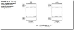
This means that the 16-bit data bus must be divided into two separate sections (or banks) that are 8 bits wide so that the microprocessor can write to either half (8-bit) or both halves (16-bit). Figure 10–27 illustrates the two banks of the memory. One bank (low bank) holds all the even- numbered memory locations, and the other bank (high bank) holds all the odd-numbered memory locations.

The 8086, 80186, 80286, and 80386SX use the BHE signal (high bank) and the A0 address bit or BLE (bus low enable) to select one or both banks of memory used for the data transfer.

Table 10–2 depicts the logic levels on these two pins and the bank or banks selected.

Bank selection is accomplished in two ways: (1) A separate write signal is developed to select a write to each bank of the memory, or (2) separate decoders are used for each bank. As a careful comparison reveals, the first technique is by far the least costly approach to memory interface for the 8086, 80186, 80286, and 80386SX microprocessors. The second technique is only used in a system that must achieve the most efficient use of the power supply.

Separate Bank Decoders. The use of separate bank decoders is often the least effective way to decode memory addresses for the 8086, 80186, 80286, and 80386SX microprocessors. This method is sometimes used, but it is difficult to understand why in most cases. One reason may be to conserve energy, because only the bank or banks selected are enabled. This is not always the case, as with the separate bank read and write signals that are discussed later.

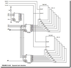
clip_image005Figure 10–28 illustrates two 74LS138 decoders used to select 64K RAM memory com- ponents for the 80386SX microprocessor (24-bit address). Here, decoder U2 has the BLE (A0) attached to G2A, and decoder U3 has the BHE signal attached to its G2A input. Because the decoder will not activate until all of its enable inputs are active, decoder U2 activates only for a 16-bit operation or an 8-bit operation from the low bank. Decoder U3 activates for a 16-bit operation

Memory Interface-0054Memory Interface-0055

or an 8-bit operation to the high bank. These two decoders and the sixteen 64K-byte RAMs they control represent a 1M range of the 80386SX memory system. Decoder U1 enables U2 and U3 for memory address range 000000H–0FFFFFH.

Notice in Figure 10–28 that the A0 address pin does not connect to the memory because it does not exist on the 80386SX microprocessor. Also notice that address bus bit position A1 is connected to memory address input A0, A2 is connected to A1, and so forth. The reason is that A0 from the 8086/80186 (or BLE from the 80286/80386SX) is already connected to decoder U2 and does not need to be connected again to the memory. If A0 or BLE is attached to the A0 address pin of memory, every other memory location in each bank of memory would be used. This means that half of the memory is wasted if A0 or BLE is connected to A0.

Memory Interface-0056

Separate Bank Write Strobes. The most effective way to handle bank selection is to develop a separate write strobe for each memory bank. This technique requires only one decoder to select a 16-bit-wide memory, which often saves money and reduces the number of components in a system.

Why not also generate separate read strobes for each memory bank? This is usually unnecessary because the 8086, 80186, 80286, and 80386SX microprocessors read only the byte of data that they need at any given time from half of the data bus. If 16-bit sections of data are always presented to the data bus during a read, the microprocessor ignores the 8-bit section that it doesn’t need, without any conflicts or special problems.

Figure 10–29 depicts the generation of separate 8086 write strobes for the memory. Here, a 74LS32 OR gate combines A0 with WR for the low bank selection signal (LWR), and BHE combines with WR for the high bank selection signal (HWR). Write strobes, for the 80286/80386SX, are generated by using the MWTC signal instead of WR.

A memory system that uses separate write strobes is constructed differently from either the 8-bit system (8088) or the system using separate memory banks. Memory in a system that uses separate write strobes is decoded as 16-bit-wide memory. For example, suppose that a memory system will contain 64K bytes of SRAM memory. This memory requires two 32K-byte memory devices (62256) so that a 16-bit-wide memory can be constructed. Because the memory is 16 bits wide and another circuit generates the bank write signals, address bit A0 becomes a don’t care. In fact, A0 is not even a pin on the 80386SX microprocessor.

Example 10–6 shows how a 16-bit-wide memory stored at locations 060000H–06FFFFH is decoded for the 80286 or 80386 microprocessor. Memory in this example is decoded, so bit A0 is a don’t care for the decoder. Bit positions A1–A15 are connected to memory component address pins A0–A14. The decoder (GAL22V10) enables both memory devices by using address connection A23–A15 to select memory whenever address 06XXXXH appears on the address bus.

Memory Interface-0057

Figure 10–30 illustrates this simple circuit by using a GAL22V10 to both decode memory and generate the separate write strobe. The program for the GAL22V10 decoder is illustrated in Example 10–7. Notice that not only is the memory selected, but both the lower and upper write strobes are also generated by the PLD.

Memory Interface-0058

Memory Interface-0059

Figure 10–31 depicts a small memory system for the 8086 microprocessor that contains an EPROM section and a RAM section. Here, there are four 27128 EPROMs (16K × 8) that com- pose a 32K × 16-bit memory at locations F0000–FFFFFH and four 62256 (32K × 8) RAMs that compose 64K × 16-bit memory at locations 00000H–1FFFFH. (Remember that even though the memory is 16 bits wide, it is still numbered in bytes.)

This circuit uses a 74HC139 dual 2-to-4 line decoder that selects EPROM with one half and RAM with the other half. It decodes memory that is 16 bits wide, not 8 bits, as before. Notice that the RD strobe is connected to all the EPROM OE inputs and all RAM OE input pins. This is done because even if the 8086 is reading only 8 bits of data, the application of the remaining 8 bits to the data bus has no effect on the operation of the 8086.

The LWR and HWR strobes are connected to different banks of the RAM memory. Here, it does matter whether the microprocessor is doing a 16-bit or an 8-bit write. If the 8086 writes a 16-bit number to memory, both LWR and HWR go low and enable the WE pins in both memory banks. But if the 8086 does an 8-bit write, only one of the write strobes goes low, writing to only one memory bank. Again, the only time that the banks make a difference is for a memory write operation.

Notice that an EPROM decoder signal is sent to the 8086 wait state generator because EPROM memory usually requires a wait state. The signal comes from the NAND gate used to select the EPROM decoder section, so that if EPROM is selected, a wait state is requested.

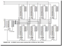
Figure 10–32 illustrates a memory system connected to the 80386SX microprocessor by using a GAL22V10 as a decoder. This interface contains 256K bytes of EPROM in the form of

Memory Interface-0060Memory Interface-0061Memory Interface-0062

four 27512 (64K × 8) EPROMs and 128K bytes of SRAM memory found in four 62256 (32K × 8) SRAMs.

Notice in Figure 10–32 that the PLD also generates the memory bank write signals LWR and HWR. As can be gleaned from this circuit, the number of components required to interface memory has been reduced to just one, in most cases (the PLD). The program listing for the PLD is located in Example 10–8. The PLD decodes the 16-bit-wide memory addresses at locations 000000H–01FFFFH for the SRAM and locations FC0000H–FFFFFFH for the EPROM.

Memory Interface-0063


MEMORY INTERFACE:8088 AND 80188 (8-BIT) MEMORY INTERFACE.

8088 AND 80188 (8-BIT) MEMORY INTERFACE

This text contains separate sections on memory interfacing for the 8088 and 80188 with their 8-bit data buses; the 8086, 80186, 80286, and 80386SX with their 16-bit data buses; the 80386DX and 80486 with their 32-bit data buses; the Pentium–Core2 with their 64-bit data buses. Separate sections are provided because the methods used to address the memory are slightly different in microprocessors that contain different data bus widths. Hardware engineers or technicians who wish to broaden their expertise in interfacing 16-bit, 32-bit, and 64-bit memory interface should cover all sections. This section is much more complete than the sections on the 16-, 32-, and 64-bit-wide memory interface, which cover material not explained in the 8088/80188 section.

In this section, we examine the memory interface to both RAM and ROM and explain the error-correction code (ECC), which is still is currently available to memory system designers. Many home computer systems do not use ECC because of the cost, but business machines often do use it.

Basic 8088/80188 Memory Interface

The 8088 and 80188 microprocessors have an 8-bit data bus, which makes them ideal to connect to the common 8-bit memory devices available today. The 8-bit memory size makes the 8088, and especially the 80188, ideal as a simple controller. For the 8088/80188 to function correctly with the memory, however, the memory system must decode the address to select a memory component. It must also use the RD, WR, and IO>M control signals provided by the 8088/80188 to control the memory system.

The minimum mode configuration is used in this section and is essentially the same as the maximum mode system for memory interface. The main difference is that, in maximum mode,the IO/M signal is combined with RD to generate the MRDC signal, and

IO/M is combined

with WR to generate the MWTC signal. The maximum mode control signals are developed inside the 8288 bus controller. In minimum mode, the memory sees the 8088 or the 80188 as a device with 20 address connections (A19–A0), eight data bus connections (AD7–AD0), and the control signals IO>M, RD, and WR.

Interfacing EPROM to the 8088. You will find this section very similar to Section 10–2 on decoders. The only difference is that, in this section, we discuss wait states and the use of the IO>M signal to enable the decoder.

Figure 10–20 illustrates an 8088/80188 microprocessor connected to three 27256 EPROMs, 32K × 8 memory devices. The 27256 has one more address input (A15) than the 27128 and twice the memory. The 74HCT138 decoder in this illustration decodes three 32K × 8 blocks of memory for a total of 96K × 8 bits of the physical address space for the 8088/80188.

The decoder (74HCT138) is connected a little differently than might be expected because the slower version of this type of EPROM has a memory access time of 450 ns. Recall from Chapter 9 that when the 8088 is operated with a 5 MHz clock, it allows 460 ns for the memory to access data. Because of the decoder’s added time delay (8 ns), it is impossible for this memory to function within 460 ns. In order to correct this problem, the output from the NAND gate can be used to generate a signal to enable the decoder and a signal for the wait state generator, covered in Chapter 9. (Note that the 80188 can internally insert from 0 to 15 wait states without any additional external hardware, so it does not require this NAND gate.) With a wait state inserted every time this section of the memory is accessed, the 8088 will allow 660 ns for the EPROM to access data. Recall that an extra wait state adds 200 ns (1 clock) to the access time. The 660 ns is ample time for a 450 ns memory component to access data, even with the delays introduced by the decoder and any buffers added to the data bus. The wait states are inserted in this system for memory locations C0000H–FFFFFH. If this creates a problem, a three-input OR gate can be added to the three outputs of the decoder to generate a wait signal only for the actual addresses for this system (E8000H–FFFFFH).

Memory Interface-0046

Notice that the decoder is selected for a memory address range that begins at location E8000H and continues through location FFFFFH—the upper 96K bytes of memory. This section of memory is an EPROM because FFFF0H is where the 8088 starts to execute instructions after a hardware reset. We often call location FFFF0H the cold-start location. The software stored in this section of memory would contain a JMP instruction at location FFFF0H that jumps to location E8000H so the remainder of the program can execute. In this circuit, U1 is decoded at addresses E8000H–EFFFFH, U2 is decoded at F0000H–F7FFFH, and U3 is decoded at F8000H–FFFFFH.

Interfacing RAM to the 8088. RAM is a little easier to interface than EPROM because most RAM memory components do not require wait states. An ideal section of the memory for the RAM is the very bottom, which contains vectors for interrupts. Interrupt vectors (discussed in more detail in Chapter 12) are often modified by software packages, so it is rather important to encode this section of the memory with RAM.

Figure 10–21 shows sixteen 62256, 32K × 8 static RAMs interfaced to the 8088, beginning at memory location 00000H. This circuit board uses two decoders to select the 16 different RAM memory components and a third to select the other decoders for the appropriate memory sections. Sixteen 32K RAMs fill memory from location 00000H through location 7FFFFH, for 512K bytes of memory.

The first decoder (U4) in this circuit selects the other two decoders. An address beginning with 00 selects decoder U3 and an address that begins with 01 selects decoder U9. Notice that extra pins remain at the output of decoder U4 for future expansion. These pins allow more 256K × 8 blocks of RAM for a total of 1M × 8, simply by adding the RAM and the additional secondary decoders.

Also notice from the circuit in Figure 10–21 that all the address inputs to this section of memory are buffered, as are the data bus connections and control signals RD and WR. Buffering is important when many devices appear on a single board or in a single system. Suppose that three other boards like this are plugged into a system. Without the buffers on each board, the load on the system address, data, and control buses would be enough to prevent proper operation. (Excessive loading causes the logic 0 output to rise above the 0.8 V maximum allowed in a sys- tem.) Buffers are normally used if the memory will contain additions at some future date. If the memory will never grow, then buffers may not be needed.

Memory Interface-0047

Interfacing Flash Memory

Flash memory (EEPROM) is becoming commonplace for storing setup information on video cards, as well as for storing the system BIOS in the personal computer. It even finds application in MP3 audio players and USB pen drives. Flash memory is also found in many other applications to store information that is only changed occasionally.

The only difference between a flash memory device and SRAM is that the flash memory device requires a 12V programming voltage to erase and write new data. The 12V can be avail- able either at the power supply or a 5V to 12V converter designed for use with flash memory can be obtained. The newest versions of flash memory are erased with a 5.0V or even a 3.3V signal so that a converter is not needed.

EEPROM is available as either a memory device with a parallel interface or as devices that are serial. The serial device is extremely small and is not suited for memory expansion, but as an I/O device it can store information such as in a flash drive. This section of the text details both memory types.

Figure 10–22 illustrates the 28F400 Intel flash memory device interfaced to the 8088 micro- processor using its parallel interface. The 28F400 can be used as either a 512K × 8 memory device or as a 256K × 16 memory device. Because it is interfaced to the 8088, its configuration is 512K × 8. Notice that the control connections on this device are identical to that of an SRAM: CE, OE, and WE. The only new pins are VPP, which is connected to 12V for erase and programming; PWD, which selects the power-down mode when a logic 0 and is also used for programming; and BYTE, which selects byte (0) or word (1) operation. Note that the pin DQ15 functions as the least significant address input when operated in the byte mode. Another difference is the amount of time required to accomplish a write operation. The SRAM can perform a write operation in as little as 10 ns, but the flash memory requires approximately 0.4 seconds to erase a byte. The topic of programming the flash memory device is covered in Chapter 11, along with I/O devices. The flash memory device has internal registers that are programmed by using I/O techniques not yet explained. This chapter concentrates on its interface to the microprocessor.

Notice in Figure 10–22 that the decoder chosen is the 74LS139 because only a simple decoder is needed for a flash memory device this large. The decoder uses address connection A19 and IO>M as inputs. The A15 signal selects the flash memory for locations 80000H through FFFFFH, and IO>M enables the decoder.

Memory Interface-0048Memory Interface-0049

As mentioned, many newer flash memory devices use a serial interface to reduce the cost of the integrated circuit because of fewer pins and a smaller size. Serial flash memory is available in sizes to 4G bytes and has comparable speeds and erase times with the parallel flash devices. Most modern flash memory functions from 5V or 3.3V without the need for a higher programming voltage and has a life of 1,000,000 erases with a storage time of 200 years.

Figure 10–23 illustrates a small serial flash device (a 256K device, organized as a 32K × 8 memory). The three address pins are hardwired to allow more than one device to be placed on a serial bus. In the illustration U1 is wired at address 001 and U2 is wired at address 000. Not shown in the illustration is a pull-up resistor that is needed for the serial data connection. The pull-up may be located in the microprocessor or it may need to be connected externally, depending on the microprocessor and interface connected to the memory.

This memory interface has two signal lines. One is a serial clock (SCL) and the other is a bidirectional serial data line (SDA). The clock frequency can be anything up to 400 KHz, so this type of memory is not meant to replace the main memory in a system. It is fast enough for music or other low-speed data. The serial interface is explained in Chapter 11.

Figure 10–24 depicts the basic serial data format for the serial EEPROM. The serial data contains the address (the A0, A1, A2 pins) in the first byte as well as a device code of 1010, which represents the EEPROM. Other serial devices have different device codes. This is followed by the memory location and the data in additional bytes.

Error Correction

Error-correction schemes have been around for a long time, but integrated circuit manufacturers have only recently started to produce error-correcting circuits. One such circuit is the 74LS636, an 8-bit error correction and detection circuit that corrects any single-bit memory read error and flags any 2-bit error called SECDED (single error correction/double error correction). This device is found in high-end computer systems because of the cost of implementing a system that uses error correction.

The newest computer systems are now using DDR memory with ECC (error-correction code). The scheme to correct the errors that might occur in these memory devices is identical to the scheme discussed in this text.

Memory Interface-0050

The 74LS636 corrects errors by storing five parity bits with each byte of memory data. This does increase the amount of memory required, but it also provides automatic error correction for single-bit errors. If more than two bits are in error, this circuit may not detect it. Fortunately, this is rare, and the extra effort required to correct more than a single-bit error is very expensive and not worth the effort. Whenever a memory component fails completely, its bits are all high or all low. In this case, the circuit flags the processor with a multiple-bit error indication.

Figure 10–25 depicts the pin-out of the 74LS636. Notice that it has eight data I/O pins, five check bit I/O pins, two control inputs (SO and SI), and two error outputs: single-error flag (SEF) and double-error flag (DEF). The control inputs select the type of operation to be performed and are listed in the truth table of Table 10–1.

When a single error is detected, the 74LS636 goes through an error-correction cycle. It places a 01 on S0 and S1 by causing a wait and then a read following error correction.

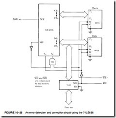
Figure 10–26 illustrates a circuit used to correct single-bit errors with the 74LS636 and to interrupt the processor through the NMI pin for double-bit errors. To simplify the illustration, we depict only one 2K × 8 RAM and a second 2K × 8 RAM to store the 5-bit check code. The connection of this memory component is different from that of the previous example. Notice that the S or CS pin is grounded, and data bus buffers control the flow to the sys- tem bus. This is necessary if the data are to be accessed from the memory before the RD strobe goes low.

On the next negative edge of the clock after the RD signal, the 74LS636 checks the single- error flag (SEF) to determine whether an error has occurred. If it has, a correction cycle causes the single-error defect to be corrected. If a double error occurs, an interrupt request is generated by the double-error flag (DEF) output, which is connected to the NMI pin of the microprocessor.

Modern DDR error-correction memory (ECC) does not actually have logic circuitry on board that detects and corrects errors. Since the Pentium, the microprocessor incorporates the logic circuitry to detect/correct errors provided the memory can store the extra 8 bits required for storing the ECC code. ECC memory is 72-bits wide using the additional 8 bits to store the ECC code. If an error occurs, the microprocessor runs the correction cycle to correct the error. Some memory devices such as Samsung memory also perform an internal error check. The Samsung ECC uses 3 bytes to check every 256 bytes of memory, which is far more efficient. Additional information on the Samsung ECC algorithm is available at the Samsung website.

Memory Interface-0051Memory Interface-0052


MEMORY INTERFACE:ADDRESS DECODING.

ADDRESS DECODING

In order to attach a memory device to the microprocessor, it is necessary to decode the address sent from the microprocessor. Decoding makes the memory function at a unique section or partition of the memory map. Without an address decoder, only one memory device can be connected to a microprocessor, which would make it virtually useless. In this section, we describe a few of the more common address-decoding techniques, as well as the decoders that are found in many systems.

Why Decode Memory?

When the 8088 microprocessor is compared to the 2716 EPROM, a difference in the number of address connections is apparent—the EPROM has 11 address connections and the microprocessor has 20. This means that the microprocessor sends out a 20-bit memory address whenever it  reads or writes data. Because the EPROM has only 11 address pins, there is a mismatch that must be corrected. If only 11 of the 8088’s address pins are connected to the memory, the 8088 will see only 2K bytes of memory instead of the 1M bytes that it “expects” the memory to contain. The decoder corrects the mismatch by decoding the address pins that do not connect to the memory component.

Simple NAND Gate Decoder

When the 2K × 8 EPROM is used, address connections A10–A0 of the 8088 are connected to address inputs A10–A0 of the EPROM. The remaining nine address pins (A19–A11) are connected to the inputs of a NAND gate decoder (see Figure 10–13). The decoder selects the EPROM from one of the 2K-byte sections of the 1M-byte memory system in the 8088 microprocessor.

In this circuit, a single NAND gate decodes the memory address. The output of the NAND gate is a logic 0 whenever the 8088 address pins attached to its inputs (A19–A11) are all logic 1s. The active low, logic 0 output of the NAND gate decoder is connected to the CE input pin that selects (enables) the EPROM. Recall that whenever CE is a logic 0, data will be read from the EPROM only if OE is also a logic 0. The OE pin is activated by the 8088 RD signal or the MRDC (memory read control) signal of other family members.

If the 20-bit binary address, decoded by the NAND gate, is written so that the leftmost nine bits are 1s and the rightmost 11 bits are don’t cares (X), the actual address range of the EPROM can be determined. (A don’t care is a logic 1 or a logic 0, whichever is appropriate.)

Example 10–1 illustrates how the address range for this EPROM is determined by writing down the externally decoded address bits (A19–A11) and the address bits decoded by the EPROM (A10–A0) as don’t cares. We really do not care about the address pins on the EPROM because they are internally decoded. As the example illustrates, the don’t cares are first written as 0s to locate the lowest address and then as 1s to find the highest address. Example 10–1 also shows these binary boundaries as hexadecimal addresses. Here, the 2K EPROM is decoded at memory address locations FF800H–FFFFFH. Notice that this is a 2K-byte section of the memory and is also located at the reset location for the 8086/8088 (FFFF0H), the most likely place for an EPROM in a system.

Memory Interface-0034Memory Interface-0035

Although this example serves to illustrate decoding, NAND gates are rarely used to decode memory because each memory device requires its own NAND gate decoder. Because of the excessive cost of the NAND gate decoder and inverters that are often required, this option requires that an alternate be found.

The 3-to-8 Line Decoder (74LS138)

One of the more common, although not only, integrated circuit decoders found in many microprocessor-based systems is the 74LS138 3-to-8 line decoder. Figure 10–14 illustrates this decoder and its truth table.

The truth table shows that only one of the eight outputs ever goes low at any time. For any of the decoder’s outputs to go low, the three enable inputs (G2A, G2B, and G1) must all be active. To be active, the G2A and G2B inputs must both be low (logic 0), and G1 must be high (logic 1). Once the 74LS138 is enabled, the address inputs (C, B, and A) select which output pin

Memory Interface-0036

Memory Interface-0037

goes low. Imagine eight EPROM CE inputs connected to the eight outputs of the decoder! This is a very powerful device because it selects eight different memory devices at the same time. Even today this device still finds wide application.

Sample Decoder Circuit. Notice that the outputs of the decoder, illustrated in Figure 10–15, are connected to eight different 2764 EPROM memory devices. Here, the decoder selects eight 8K- byte blocks of memory for a total memory capacity of 64K bytes. This figure also illustrates the address range of each memory device and the common connections to the memory devices. Notice that all of the address connections from the 8088 are connected to this circuit. Also, notice that the decoder’s outputs are connected to the CE inputs of the EPROMs, and the RD signal from the 8088 is connected to the OE inputs of the EPROMs. This allows only the selected EPROM to be enabled and to send its data to the microprocessor through the data bus whenever RD becomes a logic 0.

In this circuit, a three-input NAND gate is connected to address bits A19–A17. When all three address inputs are high, the output of this NAND gate goes low and enables input G2B of the 74LS138. Input G1 is connected directly to A16. In other words, in order to enable this decoder, the first four address connections (A19–A16) must all be high.

The address inputs C, B, and A connect to microprocessor address pins A15–A13. These three address inputs determine which output pin goes low and which EPROM is selected when- ever the 8088 outputs a memory address within this range to the memory system.

Example 10–2 shows how the address range of the entire decoder is determined. Notice that the range is location F0000H–FFFFFH. This is a 64K-byte span of the memory.

Memory Interface-0038

How is it possible to determine the address range of each memory device attached to the decoder’s outputs? Again, the binary bit pattern is written down; this time the C, B, and A address inputs are not don’t cares. Example 10–3 shows how output 0 of the decoder is made to go low to select the EPROM attached to that pin. Here, C, B, and A are shown as logic 0s.

Memory Interface-0039

If the address range of the EPROM connected to output 1 of the decoder is required, it is determined in exactly the same way as that of output 0. The only difference is that now the C, B, and A inputs contain a 001 instead of a 000 (see Example 10–4). The remaining output address ranges are determined in the same manner by substituting the binary address of the output pin into C, B, and A.

Memory Interface-0040

The Dual 2-to-4 Line Decoder (74LS139)

Another decoder that finds some application is the 74LS139 dua1 2-to-4 line decoder. Figure 10–16 illustrates both the pin-out and the truth table for this decoder. The 74LS139 contains two separate 2-to-4 line decoders—each with its own address, enable, and output connections.

A more complicated decoder using the 74LS139 decoder appears in Figure 10–17. This circuit uses a 128K × 8 EPROM (271000) and a 128K × 8 SRAM (621000). The EPROM is decoded at memory locations E0000H–FFFFFH and the SRAM is decoded at addresses 00000H–1FFFFH. This is fairly typical of a small embedded system, where the EPROM is located at the top of the memory space and the SRAM at the bottom.

Output Y0 of decoder U1A activates the SRAM whenever address bits A17 and A18 are both logic 0s if the IO>M signal is a logic 0 and address line A19 is a logic 0. This selects the SRAM for any address between 00000H and 1FFFFH. The second decoder (U1B) is slightly more complicated because the NAND gate (U4B) selects the decoder when IO>M is a logic 0 while A19 is a logic 1. This selects the EPROM for addresses E0000H through FFFFFH.

PLD Programmable Decoders

This section of the text explains the use of the programmable logic device, or PLD, as a decoder. There are three SPLD (simple PLD) devices that function in the same manner but have different names: PLA (programmable logic array), PAL (programmable array logic), and GAL (gated array logic). Although these devices have been in existence since the mid-1970s, they have only appeared in memory system and digital designs since the early 1990s. The PAL and the PLA are fuse-programmed, as is the PROM, and some PLD devices are erasable devices (as are EPROMs). In essence, all three devices are arrays of logic elements that are programmable.

Memory Interface-0041

Other PLDs are also available, such as CPLDs (complex programmable logic devices), FPGAs (field programmable gate arrays), and FPICs (field programmable interconnect). These types of PLDs are much more complex than the SPLDs that are used more commonly in designing a complete system. If the concentration is on decoding addresses, the SPLD is used and if the concentration is on a complete system, then the CPLD, FPLG, or FPIC is used to implement the design. These devices are also referred to as an ASIC (application-specific integrated circuit).

Combinatorial Programmable Logic Arrays. One of the two basic types of PALs is the combinatorial programmable logic array. This device is internally structured as a programmable array of combinational logic circuits. Figure 10–18 illustrates the internal structure of the PAL16L8 that is constructed with AND/OR gate logic. This device, which is representative of a PLD, has 10 fixed inputs, two fixed outputs, and six pins that are programmable as inputs of outputs. Each output sig- nal is generated from a seven-input OR gate that has an AND gate attached to each input. The out- puts of the OR gates pass through a three-state inverter that defines each output as an AND/NOR function. Initially, all of the fuses connect all of the vertical/horizontal connections illustrated in Figure 10–18. Programming is accomplished by blowing fuses to connect various inputs to the OR gate array. The wired-AND function is performed at each input connection, which allows a product term of up to 16 inputs. A logic expression using the PAL16L8 can have up to seven product terms with up to 16 inputs NORed together to generate the output expression. This device is ideal as a memory address decoder because of its structure. It is also ideal because the outputs are active low.

Fortunately, we don’t have to choose the fuses by number for programming, as was customary when this device was first introduced. A PAL is programmed with a software package such as PALASM, the PAL assembler program. More recently, PLD design is accomplished using HDL (hardware description language) or VHDL (verilog HDL). The VHDL language and its syntax are currently the industry standard for programming PLD devices. Example 10–5 shows a pro- gram that decodes the same areas of memory as decoded in Figure 10–17. Note that this program

Memory Interface-0042

was developed by using a text editor such as EDIT, available with Microsoft DOS version 7.1 with XP or NotePad in Windows. The program can also be developed by using an editor than comes with any of the many programming packages for PLDs. Various editors attempt to ease the task of defining the pins, but we believe it is easier to use NotePad and the listing as shown.

Memory Interface-0043

Memory Interface-0044

Comments in VHDL programming begin with a pair of minus signs as illustrated in the first line of the VHDL code in Example 10–5. The library and use statements specify the standard IEEE library using standard logic. The entity statement names the VHDL module, in this case DECODER_10_17. The port statements define the in, out, and in-out pins used in the equations for the logic expression, which appears in the begin block. A19, A18, A17, and MIO (this signal cannot be defined as IO>M so it was called MIO) are defined as input pins and ROM and RAM are the output pins for connection to the CS pins on the memory devices. The architecture statement merely refers to the version (V1) of this design. Finally, the equations for the design are placed in the begin block. Each output pin has its own equation. The key- word not is used for logical inversion and the keyword and is used for the logical and opera- tion. In this case the ROM equation causes the ROM pin to become a logic zero only when the A19, A18, A17, and MIO are all logic zeros (00000H–1FFFFH). The RAM equation causes the RAM pin to become a logic zero when A18 and A17 are all ones at the same time that MIO is a logic zero. A19 is connected to the active high CE2 pin after being inverted by the PLD. The RAM is selected for addresses 60000H–7FFFFH. See Figure 10–19 for the PLD realization of Example 10–5.

Memory Interface-0045


MEMORY INTERFACE:MEMORY DEVICES.

Memory Interface

INTRODUCTION

Whether simple or complex, every microprocessor-based system has a memory system. The Intel family of microprocessors is no different from any other in this respect. Almost all systems contain two main types of memory: read-only memory (ROM) and random access memory (RAM) or read/write memory. Read-only memory contains system software and permanent system data, while RAM contains temporary data and application software. This chapter explains how to interface both memory types to the Intel family of microprocessors. We demonstrate memory interface to an 8-, 16-, 32-, and 64-bit data bus by using various memory address sizes. This allows virtually any microprocessor to be interfaced to any memory system.

CHAPTER OBJECTIVES

Upon completion of this chapter, you will be able to:

1. Decode the memory address and use the outputs of the decoder to select various memory components.

2. Use programmable logic devices (PLDs) to decode memory addresses.

3. Explain how to interface both RAM and ROM to a microprocessor.

4. Explain how error correction code (ECC) is used with memory.

5. Interface memory to an 8-, 16-, 32-, and 64-bit data bus.

6. Explain the operation of a dynamic RAM controller.

7. Interface dynamic RAM to the microprocessor.

MEMORY DEVICES

Before attempting to interface memory to the microprocessor, it is essential to completely under- stand the operation of memory components. In this section, we explain the functions of the four common types of memory: read-only memory (ROM), flash memory (EEPROM), static random access memory (SRAM), and dynamic random access memory (DRAM).

Memory Pin Connections

Pin connections common to all memory devices are the address inputs, data outputs or input/ outputs, some type of selection input, and at least one control input used to select a read or write operation. See Figure 10–1 for ROM and RAM generic-memory devices.

Address Connections. All memory devices have address inputs that select a memory location within the memory device. Address inputs are almost always labeled from A0, the least significant address input, to An where subscript n can be any value but is always labeled as one less than the total number of address pins. For example, a memory device with 10 address pins has its address pins labeled from A0 to A9. The number of address pins found on a memory device is determined by the number of memory locations found within it.

Today, the more common memory devices have between 1K (1024) to 1G (1,073,741,824) memory locations, with 4G and larger memory location devices on the horizon. A 1K memory device has 10 address pins (A0–A9); therefore, 10 address inputs are required to select any of its 1024 memory locations. It takes a 10-bit binary number (1024 different combinations) to select any single location on a 1024-location device. If a memory device has 11 address connections (A0–A11), it has 2048 (2K) internal memory locations. The number of memory locations can thus be extrapolated from the number of address pins. For example, a 4K memory device has 12 address connections, an 8K device has 13, and so forth. A device that contains 1M locations requires a 20-bit address (A0–A19).

The number 400H represents a 1K-byte section of the memory system. If a memory device is decoded to begin at memory address 10000H and it is a 1K device, its last location is at address 103FFH—one location less than 400H. Another important hexadecimal number to remember is 1000H, because 1000H is 4K. A memory device that contains a starting address of 14000H that is 4K bytes long ends at location 14FFFH—one location less than 1000H. A third number is 64K, or 10000H. A memory that starts at location 30000H and ends at location 3FFFFH is a 64K-byte memory. Finally, because 1M of memory is common, a 1M memory contains 100000H memory locations.

Data Connections. All memory devices have a set of data outputs or input/outputs. The device illustrated in Figure 10–1 has a common set of input/output (I/O) connections. Today, many memory devices have bidirectional common I/O pins.

The data connections are the points at which data are entered for storage or extracted for reading. Data pins on memory devices are labeled D0 through D7 for an 8-bit-wide memory

Memory Interface-0023

device. In this sample memory device there are 8 I/O connections, meaning that the memory device stores 8 bits of data in each of its memory locations. An 8-bit-wide memory device is often called a byte-wide memory. Although most devices are currently 8 bits wide, some devices are 16 bits, 4 bits, or just 1 bit wide.

Catalog listings of memory devices often refer to memory locations times bits per location. For example, a memory device with 1K memory locations and 8 bits in each location is often listed as a 1K × 8 by the manufacturer. A 16K × 1 is a memory device containing 16K 1-bit memory locations. Memory devices are often classified according to total bit capacity. For example, a 1K × 8-bit memory device is sometimes listed as an 8K memory device, or a 64K × 4 memory is listed as a 256K device. These variations occur from one manufacturer to another.

election Connections. Each memory device has an input—sometimes more than one—that selects or enables the memory device. This type of input is most often called a chip select (CS), chip enable (CE), or simply select (S) input. RAM memory generally has at least one CS or S input, and ROM has at least one CE. If the CE, CS, or S input is active (a logic 0, in this case, because of the overbar), the memory device performs a read or write operation; if it is inactive (a logic 1, in this case), the memory device cannot do a read or a write because it is turned off or disabled. If more than one CS connection is present, all must be activated to read or write data.

Control Connections. All memory devices have some form of control input or inputs. A ROM usually has only one control input, while a RAM often has one or two control inputs.

The control input most often found on a ROM is the output enable (OE) or gate (G) connection, which allows data to flow out of the output data pins of the ROM. If OE and the selection input (CE) are both active, the output is enabled; if OE is inactive, the output is disabled at its high-impedance state. The OE connection enables and disables a set of three-state buffers located within the memory device and must be active to read data.

A RAM memory device has either one or two control inputs. If there is only one control input, it is often called R>W. This pin selects a read operation or a write operation only if the device is selected by the selection input (CS). If the RAM has two control inputs, they are usually labeled WE (or W), and OE (or G). Here, WE (write enable) must be active to perform a memory write, and OE must be active to perform a memory read operation. When these two controls (WE and OE) are pre- sent, they must never both be active at the same time. If both control inputs are inactive (logic 1s), data are neither written nor read, and the data connections are at their high-impedance state.

ROM Memory

The read-only memory (ROM) permanently stores programs and data that are resident to the sys- tem and must not change when power supply is disconnected. The ROM is permanently programmed so that data are always present, even when power is disconnected. This type of memory is often called nonvolatile memory, because its contents do not change even if power is disconnected.

Today, the ROM is available in many forms. A device we call a ROM is purchased in mass quantities from a manufacturer and programmed during its fabrication at the factory. The EPROM (erasable programmable read-only memory), a type of ROM, is more commonly used when software must be changed often or when too few are in demand to make the ROM economical. For a ROM to be practical, we usually must purchase at least 10,000 devices to recoup the factory programming charge. An EPROM is programmed in the field on a device called an EPROM programmer. The EPROM is also erasable if exposed to high-intensity ultra- violet light for about 20 minutes or so, depending on the type of EPROM.

PROM memory devices are also available, although they are not as common today. The PROM (programmable read-only memory) is also programmed in the field by burning open tiny NI-chrome or silicon oxide fuses; but once it is programmed, it cannot be erased.
Memory Interface-0024

Still another, newer type of read-mostly memory (RMM) is called the flash memory. The flash memory1 is also often called an EEPROM (electrically erasable programmable ROM), EAROM (electrically alterable ROM), or a NOVRAM (nonvolatile RAM). These memory devices are electrically erasable in the system, but they require more time to erase than a normal RAM. The flash memory device is used to store setup information for systems such as the video card in the computer. It has all but replaced the EPROM in most computer systems for the BIOS memory. Some systems contain a password stored in the flash memory device. Flash memory has its biggest impact in memory cards for digital cameras and memory in MP3 audio players.

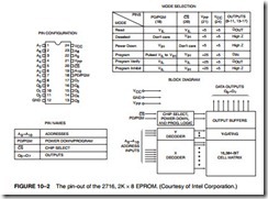
Figure 10–2 illustrates the 2716 EPROM, which is representative of most common EPROMs. This device contains 11 address inputs and eight data outputs. The 2716 is a 2K × 8 read-only memory device. The 27XXX series of the EPROMs includes the following part numbers: 2704 (512 × 8), 2708 (1K × 8), 2716 (2K × 8), 2732 (4K × 8), 2764 (8K × 8), 27128 (16K × 8), 27256 (32K × 8), 27512 (64K × 8), and 271024 (128K × 8). Each of these parts contains address pins, eight data connections, one or more chip selection inputs (CE), and an output enable pin (OE).

Figure 10–3 illustrates the timing diagram for the 2716 EPROM. Data appear on the out- put connections only after a logic 0 is placed on both CE and OE pin connections. If CE and OE are not both logic 0s, the data output connections remain at their high-impedance or off states. Note that the VPP pin must be placed at a logic 1 level for data to be read from the EPROM. In some cases, the VPP pin is in the same position as the WE pin on the SRAM. This will allow a single socket to hold either an EPROM or an SRAM. An example is the 27256 EPROM and the 62256 SRAM, both 32K × 8 devices that have the same pin-out, except for VPP on the EPROM and WE on the SRAM.

Memory Interface-0025

One important piece of information provided by the timing diagram and data sheet is the memory access time—the time that it takes the memory to read information. As Figure 10–3 illustrates, memory access time (TACC) is measured from the appearance of the address at the address inputs until the appearance of the data at the output connections. This is based on the assumption that the CE input goes low at the same time that the address inputs become stable. Also, OE must be a logic 0 for the output connections to become active. The basic speed of this EPROM is 450 ns. (Recall that the 8086/8088 operated with a 5 MHz clock allowed memory 460 ns to access data.) This type of memory component requires wait states to operate properly with the 8086/8088 microprocessors because of its rather long access time. If wait states are not desired, higher-speed versions of the EPROM are available at an additional cost. Today, EPROM memory is available with access times of as little as 100 ns. Obviously, wait states are required in modern microprocessors for any EPROM device.

Static RAM (SRAM) Devices

Static RAM memory devices retain data for as long as DC power is applied. Because no special action (except power) is required to retain stored data, these devices are called static memory. They are also called volatile memory because they will not retain data without power. The main

Memory Interface-0026

difference between a ROM and a RAM is that a RAM is written under normal operation, whereas a ROM is programmed outside the computer and normally is only read. The SRAM, which stores temporary data, is used when the size of the read/write memory is relatively small. Today, a small memory is one that is less than 1M byte.

Figure 10–4 illustrates the 4016 SRAM, which is a 2K × 8 read/write memory. This device has 11 address inputs and eight data input/output connections. This device is representative of all SRAM devices, except for the number of address and data connections.

The control inputs of this RAM are slightly different from those presented earlier. The OE pin is labeled G, the CS pin is S, and the WE pin is W. Despite the altered designations, the con- trol pins function exactly the same as those outlined previously. Other manufacturers make this popular SRAM under the part numbers 2016 and 6116.

Figure 10–5 depicts the timing diagram for the 4016 SRAM. As the read cycle timing reveals, the access time is ta(A). On the slowest version of the 4016, this time is 250 ns, which is fast enough to connect directly to an 8088 or an 8086 operated at 5 MHz without wait states.

Again, it is important to remember that the access time must be checked to determine the compatibility of memory components with the microprocessor.

Figure 10–6 on p. 336 illustrates the pin-out of the 62256, 32K × 8 static RAM. This device is packaged in a 28-pin integrated circuit and is available with access times of 120 ns or 150 ns. Other common SRAM devices are available in 8K × 8, 128K × 8, 256K × 8, 512K × 8, and 1M × 8 sizes, with access times of as little as 1.0 ns for SRAM used in computer cache memory systems.

Dynamic RAM (DRAM) Memory

About the largest static RAM available today is a 1M × 8. Dynamic RAM, on the other hand, is available in much larger sizes: up to 256M × 8 (2G bits). In all other respects, DRAM is essentially the same as SRAM, except that it retains data for only 2 or 4 ms on an integrated capacitor. After 2 or 4 ms, the contents of the DRAM must be completely rewritten (refreshed) because the capacitors, which store a logic 1 or logic 0, lose their charges.

Instead of requiring the almost impossible task of reading the contents of each memory location with a program and then rewriting them, the manufacturer has internally constructed the DRAM differently from the SRAM. In the DRAM, the entire contents of the memory are refreshed with 256 reads in a 2- or 4-ms interval. Refreshing also occurs during a write, a read, or during a special refresh cycle. Much more information about DRAM refreshing is provided in Section 10–6.

Another disadvantage of DRAM memory is that it requires so many address pins that the manufacturers have decided to multiplex the address inputs. Figure 10–7 illustrates a 64K × 4 DRAM, the TMS4464, which stores 256K bits of data. Notice that it contains only eight address inputs where it should contain 16—the number required to address 64K memory locations. The

Memory Interface-0027

Memory Interface-0028Memory Interface-0029

inputs and strobed into an internal column latch by CAS as the column address (see Figure 10–8 for this timing). The 16-bit address held in these internal latches addresses the contents of one of the 4-bit memory locations. Note that CAS also performs the function of the chip selection input to the DRAM.

Figure 10–9 illustrates a set of multiplexers used to strobe the column and row addresses into the eight address pins on a pair of TMS4464 DRAMs. Here, the RAS signal not only strobes

Memory Interface-0030

Memory Interface-0031

the row address into the DRAMs, but it also selects which part of the address is applied to the address inputs. This is possible due to the long propagation-delay time of the multiplexers. When RAS is a logic 1, the B inputs are connected to the Y outputs of the multiplexers; when the RAS input goes to a logic 0, the A inputs connect to the Y outputs. Because the internal row address latch is edge-triggered, it captures the row address before the address at the inputs changes to the column address. More detail on DRAM and DRAM interfacing is provided in Section 10–6.

As with the SRAM, the R>W pin writes data to the DRAM when a logic 0, but there is no pin labeled G or enable. There also is no S (select) input to the DRAM. As mentioned, the CAS input selects the DRAM. If selected, the DRAM is written if R>W 0 and read if R>W 1.

Figure 10–10 shows the pin-out of the 41256 dynamic RAM. This device is organized as a 256K × 1 memory, requiring as little as 70 ns to access data.

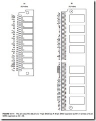
More recently, larger DRAMs have become available that are organized as a 16M × 1, 256M × 1, 512M × 1, 1G × 1, and 2G × 1 memory. On the horizon is the 4G × 1 memory, which is in the planning stages. DRAM memory is often placed on small circuit boards called SIMMs (Single In-Line Memory Modules). Figure 10–11 shows the pin-outs of the two most common SIMMs. The 30-pin SIMM is organized most often as 1M × 8 or 1M × 9, and 4M × 8 or 4M × 9. (Illustrated in Figure 10–11 is a 4M × 9.) The ninth bit is the parity bit. Also shown is a newer 72 pin SIMM. The 72-pin SIMMs are often organized as 1M × 32 or 1M × 36 (with parity). Other sizes are 2M × 32, 4M × 32, 8M × 32, and 16M × 32. These are also available with parity. Figure 10–11 illustrates a 4M × 36 SIMM, which has 16M bytes of memory.

Lately, many systems are using the Pentium–Pentium 4 microprocessors. These micro- processors have a 64-bit wide data bus, which precludes the use of the 8-bit-wide SIMMs described here. Even the 72-pin SIMMs are cumbersome to use because they must be used in pairs to obtain a 64-bit-wide data connection. Today, the 64-bit-wide DIMMs (Dual In-line Memory Modules) have become the standard in most systems. The memory on these modules is organized as 64 bits wide. The common sizes available are 16M bytes (2M × 64), 32M bytes (4M × 64), 64M bytes (8M × 64), 128M bytes (16M × 64), 256M bytes (32M × 64), 512M bytes (64M × 64), and 1G bytes (128M × 64). The pin-out of the DIMM is illustrated in Figure 10–12.

The DIMM module is available in DRAM, EDO, SDRAM, and DDR (double-data rate) forms,
Memory Interface-0032

Memory Interface-0033

with or without an EPROM. The EPROM provides information to the system on the size and the speed of the memory device for plug-and-play applications.

Another addition to the memory market is the RIMM memory module from RAMBUS Corporation, although this memory type has faded from the market. Like the SDRAM, the RIMM contains 168 pins, but each pin is a two-level pin, bringing the total number of connections to 336. The fastest SDRAM currently available is the PC-4400 or 500 DDR, which operates at a rate of 4.4G bytes per second. By comparison, the 800 MHz RIMM operates at a rate of 3.2G bytes per second and is no longer supported in many systems. RDRAM had a fairly short life in the volatile computer market. The RIMM module is organized as a 32-bit-wide device. This means that to populate a Pentium 4 memory, RIMM memory is used in pairs. Intel claims that the Pentium 4 system using RIMM modules is 300% faster than a Pentium III using PC-100 memory. According to RAMBUS, the current 800 MHz RIMM has been increased to a speed of 1200 MHz, but it is still not fast enough to garner much of a market share.

Currently the latest DRAM is the DDR (double-data rate) memory device and DDR2. The DDR memory transfers data at each edge of the clock, making it operate at twice the speed of SDRAM. This does not affect the access time for the memory, so many wait states are still required to operate this type of memory, but it can be much faster than normal SDRAM memory and that includes RDRAM.


SUMMARY OF 8086/8088 HARDWARE SPECIFICATIONS.

SUMMARY

1. The main differences between the 8086 and 8088 are (1) an 8-bit data bus on the 8088 and a 16-bit data bus on the 8086, (2) an SS0 pin on the 8088 in place of BHE /S7 on the 8086, and (3) an IO/M pin on the 8088 instead of an M/ IO on the 8086.

2. Both the 8086 and 8088 require a single +5.0 V power supply with a tolerance of ±10%.

3. The 8086/8088 microprocessors are TTL-compatible if the noise immunity figure is derated to 350 mV from the customary 400 mV.

4. The 8086/8088 microprocessors can drive one 74XX, five 74LSXX, one 74SXX, ten 74ALSXX, and ten 74HCXX unit loads.

5. The 8284A clock generator provides the system clock (CLK), READY synchronization, and RESET synchronization.

6. The standard 5 MHz 8086/8088 operating frequency is obtained by attaching a 15 MHz crystal to the 8284A clock generator. The PCLK output contains a TTL-compatible signal at one half the CLK frequency.

7. Whenever the 8086/8088 microprocessors are reset, they begin executing software at memory location FFFF0H (FFFF:0000) with the interrupt request pin disabled.

8. Because the 8086/8088 buses are multiplexed and most memory and I/O devices aren’t, the system must be demultiplexed before interfacing with memory or I/O. Demultiplexing is accomplished by an 8-bit latch whose clock pulse is obtained from the ALE signal.

9. In a large system, the buses must be buffered because the 8086/8088 microprocessors are capable of driving only 10 unit loads, and large systems often have many more.

10. Bus timing is very important to the remaining chapters in the text. A bus cycle that consists of four clocking periods acts as the basic system timing. Each bus cycle is able to read or write data between the microprocessor and the memory or I/O system.

11. A bus cycle is broken into four states, or T periods: T1 is used by the microprocessor to send the address to the memory or I/O and the ALE signal to the demultiplexers; T2 is used to send data to memory for a write and to test the READY pin and activate control signals RD or WR; T3 allows the memory time to access data and allows data to be transferred between the microprocessor and the memory or I/O; and T4 is where data are written.

12. The 8086/8088 microprocessors allow the memory and I/O 460 ns to access data when they are operated with a 5 MHz clock.

13. Wait states (Tw) stretch the bus cycle by one or more clocking periods to allow the memory and I/O additional access time. Wait states are inserted by controlling the READY input to the 8086/8088. READY is sampled at the end of T2 and during Tw.

14. Minimum mode operation is similar to that of the Intel 8085A microprocessor, whereas maximum mode operation is new and specifically designed for the operation of the 8087 arithmetic coprocessor.

15. The 8288 bus controller must be used in the maximum mode to provide the control bus signals to the memory and I/O. This is because the maximum mode operation of the 8086/8088 removes some of the system’s control signal lines in favor of control signals for the coprocessors. The 8288 reconstructs these removed control signals.


QUESTIONS AND PROBLEMS ON 8086/8088 HARDWARE SPECIFICATIONS.

QUESTIONS AND PROBLEMS

1. List the differences between the 8086 and the 8088 microprocessors.

2. Is the 8086/8088 TTL-compatible? Explain your answer.

3. What is the fan-out from the 8086/8088 to the following devices:

(a) 74XXX TTL

(b) 74ALSXXX TTL

(c) 74HCXXX CMOS

4. What information appears on the address/data bus of the 8088 while ALE is active?

5. What are the purposes of status bits S3 and S4?

6. What condition does a logic 0 on the 8086/8088 RD pin indicate?

7. Zxplain the operation of the TEST pin and the WAIT instruction.

8. Describe the signal that is applied to the CLK input pin of the 8086/8088 microprocessors.

9. What mode of operation is selected when MN>MX is grounded?

10. What does the WR strobe signal from the 8086/8088 indicate about the operation of the 8086/8088?

11. When does ALE float to its high-impedance state?

12. When DT>R is a logic 1, what condition does it indicate about the operation of the 8086/8088?

13. What happens when the HOLD input to the 8086/8088 is placed at its logic 1 level?

14. What three minimum mode 8086/8088 pins are decoded to discover whether the processor is halted?

15. Explain the operation of the LOCK pin.

16. What conditions do the QS1 and QS0 pins indicate about the 8086/8088?

17. What three housekeeping chores are provided by the 8284A clock generator?

18. By what factor does the 8284A clock generator divide the crystal oscillator’s output frequency?

19. If the F>C pin is placed at a logic 1 level, the crystal oscillator is disabled. Where is the timing input signal attached to the 8284A under this condition?

20. The PCLK output of the 8284A is MHz if the crystal oscillator is operating at 14 MHz.

The RES input to the 8284A is placed at a logic level in order to reset the 8086/8088.

22. Which bus connections on the 8086 microprocessor are typically demultiplexed?

23. Which bus connections on the 8088 microprocessor are typically demultiplexed?

24. Which TTL-integrated circuit is often used to demultiplex the buses on the 8086/8088?

25. What is the purpose of the demultiplexed BHE signal on the 8086 microprocessor?

26. Why are buffers often required in an 8086/8088-based system?

27. What 8086/8088 signal is used to select the direction of the data flows through the 74LS245 bidirectional bus buffer?

28. A bus cycle is equal to clocking periods.

29. If the CLK input to the 8086/8088 is 4 MHz, how long is one bus cycle?

30. What two 8086/8088 operations occur during a bus cycle?

31. How many MIPS is the 8086/8088 capable of obtaining when operated with a 10 MHz clock?

32. Briefly describe the purpose of each T state listed:

(a) T1

(b) T2

(c) T3

(d) T4

(e) Tw

33. How much time is allowed for memory access when the 8086/8088 is operated with a 5 MHz clock?

How wide is DEN if the 8088 is operated with a 5 MHz clock?

35. If the READY pin is grounded, it will introduce states into the bus cycle of the 8086/8088.

36. What does the ASYNC input to the 8284A accomplish?

37. What logic levels must be applied to AEN1 and RDY1 to obtain a logic 1 at the READY pin? (Assume that AEN2 is at a logic 1 level.)

38. Contrast minimum and maximum mode 8086/8088 operation.

39. What main function is provided by the 8288 bus controller when used with 8086/8088 maximum mode operation?


8086/8088 HARDWARE SPECIFICATIONS:MINIMUM MODE VERSUS MAXIMUM MODE.

MINIMUM MODE VERSUS MAXIMUM MODE

There are two available modes of operation for the 8086/8088 microprocessors: minimum mode and maximum mode. Minimum mode operation is obtained by connecting the mode selection pin MN>MX to +5.0 V, and maximum mode is selected by grounding this pin. Both modes enable different control structures for the 8086/8088 microprocessors. The mode of operation provided by minimum mode is similar to that of the 8085A, the most recent Intel 8-bit micro- processor. The maximum mode is unique and designed to be used whenever a coprocessor exists in a system. Note that the maximum mode was dropped from the Intel family beginning with the 80286 microprocessor.

Minimum Mode Operation

Minimum mode operation is the least expensive way to operate the 8086/8088 microprocessors (see Figure 9–19 for the minimum mode 8088 system). It costs less because all the control sig- nals for the memory and I/O are generated by the microprocessor. These control signals are identical to those of the Intel 8085A, an earlier 8-bit microprocessor. The minimum mode allows the 8085A 8-bit peripherals to be used with the 8086/8088 without any special considerations.

Maximum Mode Operation

Maximum mode operation differs from minimum mode in that some of the control signals must be externally generated. This requires the addition of an external bus controller—the 8288 bus controller (see Figure 9–20 for the maximum mode 8088 system). There are not enough pins on the 8086/8088 for bus control during maximum mode because new pins and new features have replaced some of them. Maximum mode is used only when the system contains external coprocessors such as the 8087 arithmetic coprocessor.

8086-8088 Hardware Specifications-00208086-8088 Hardware Specifications-0021

The 8288 Bus Controller

An 8086/8088 system that is operated in maximum mode must have an 8288 bus controller to provide the signals eliminated from the 8086/8088 by the maximum mode operation. Figure 9–21 illustrates the block diagram and pin-out of the 8288 bus controller.

Notice that the control bus developed by the 8288 bus controller contains separate signals for I/O (IORC and IOWC) and memory (MRDC and MWTC). It also contains advanced memory (AMWC) and I/O (AIOWC) write strobes, and the INTA signal. These signals replace the minimum mode ALE, WR, IO/M, DT/R, DEN, and INTA, which are lost when the 8086/8088 microprocessors are operated in the maximum mode.

8086-8088 Hardware Specifications-0022

Pin Functions

The following list provides a description of each pin of the 8288 bus controller.

S2, S1, and S0 Status inputs are connected to the status output pins on the 8086/8088 microprocessor. These three signals are decoded to generate the timing signals for the system.

CLK The clock input provides internal timing and must be connected to the CLK output pin of the 8284A clock generator.

ALE The address latch enable output is used to demultiplex the address/data bus.

DEN The data bus enable pin controls the bidirectional data bus buffers in the system. Note that this is an active high output pin that is the opposite polarity from the DEN signal found on the microprocessor when operated in the minimum mode.

DT>R AEN

The data transmit/receive signal is output by the 8288 to control the direction of the bidirectional data bus buffers.

The address enable input causes the 8288 to enable the memory control signals.

CEN The control enable input enables the command output pins on the 8288.

IOB The I/O bus mode input selects either the I/O bus mode or system bus mode operation.

AIOWC

IORC IOWC AMWT

MWTC MRDC

INTA

MCE>PDEN

The advanced I/O write is a command output used to provide I/O with an advanced I/O write control signal.

The I/O read command output provides I/O with its read control signal. The I/O write command output provides I/O with its main write signal. The advanced memory write control pin provides memory with an early or advanced write signal.

The memory write control pin provides memory with its normal write control signal.

The memory read control pin provides memory with a read control signal. The interrupt acknowledge output acknowledges an interrupt request input applied to the INTR pin.

The master cascade/peripheral data output selects cascade operation for an interrupt controller if IOB is grounded, and enables the I/O bus transceivers if IOB is tied high.


8086/8088 HARDWARE SPECIFICATIONS:READY AND THE WAIT STATE.

READY AND THE WAIT STATE

As we mentioned earlier in this chapter, the READY input causes wait states for slower memory and I/O components. A wait state (Tw) is an extra clocking period, inserted between T2 and T3 to lengthen the bus cycle. If one wait state is inserted, then the memory access time, normally 460 ns with a 5 MHz clock, is lengthened by one clocking period (200 ns) to 660 ns.

In this section, we discuss the READY synchronization circuitry inside the 8284A clock generator, show how to insert one or more wait states selectively into the bus cycle, and examine the READY input and the synchronization times it requires.

The READY Input

The READY input is sampled at the end of T2 and again, if applicable, in the middle of Tw. If READY is a logic 0 at the end of T2, T3 is delayed and Tw is inserted between T2 and T3. READY is next sampled at the middle of Tw to determine whether the next state is Tw or T3. It is tested for a logic 0 on the 1-to-0 transition of the clock at the end of T2, and for a 1 on the 0-to-1 transition of the clock in the middle of Tw.

The READY input to the 8086/8088 has some stringent timing requirements. The timing diagram in Figure 9–14 shows READY causing one wait state (Tw), along with the required setup and hold times from the system clock. The timing requirement for this operation is met by the internal READY synchronization circuitry of the 8284A clock generator. When the 8284A is used for READY, the RDY (ready input to the 8284A) input occurs at the end of each T state.

RDY and the 8284A

RDY is the synchronized ready input to the 8284A clock generator. The timing diagram for this input is provided in Figure 9–15. Although it differs from the timing for the READY input to the

8086-8088 Hardware Specifications-00178086-8088 Hardware Specifications-0018

8086/8088, the internal 8284A circuitry guarantees the accuracy of the READY synchronization provided to the 8086/8088 microprocessors.

Figure 9–16 again depicts the internal structure of the 8284A. The bottom half of this diagram is the READY synchronization circuitry. At the leftmost side, the RDY1 and AEN1 inputs are ANDed, as are the RDY2 and AEN2 inputs. The outputs of the AND gates are then ORed to generate the input to the one or two stages of synchronization. In order to obtain a logic 1 at the inputs to the flip-flops, RDY1 ANDed with AEN1 must be active or RDY2 ANDed with AEN2 must be active.

The ASYNC input selects one stage of synchronization when it is a logic 1 and two stages when it is a logic 0. If one stage is selected, then the RDY signal is kept from reaching the 8086/8088 READY pin until the next negative edge of the clock. If two stages are selected, the first positive edge of the clock captures RDY in the first flip-flop. The output of this flip-flop is fed to the second flip-flop, so on the next negative edge of the clock, the second flip-flop captures RDY.

Figure 9–17 illustrates a circuit used to introduce almost any number of wait states for the 8086/8088 microprocessors. Here, an 8-bit serial shift register (74LS164) shifts a logic 0 for one or more clock periods from one of its Q outputs through to the RDY1 input of the 8284A. With appropriate strapping, this circuit can provide various numbers of wait states. Notice also how the shift register is cleared back to its starting point. The output of the register is forced high when the RD, WR, and INTA pins are all logic 1s. These three signals are high until state T2, so the shift register shifts for the first time when the positive edge of the T2 arrives. If one wait is desired, output QB is connected to the OR gate. If two waits are desired, output QC is connected, and so forth.

Notice in Figure 9–17 that this circuit does not always generate wait states. It is enabled from the memory only for memory devices that require the insertion of waits. If the selection signal from a memory device is a logic 0, the device is selected; then this circuit will generate a wait state.

Figure 9–18 illustrates the timing diagram for this shift register wait state generator when it is wired to insert one wait state. The timing diagram also illustrates the internal contents of the shift register’s flip-flops to present a more detailed view of its operation. In this example, one wait state is generated.

8086-8088 Hardware Specifications-0019


8086/8088 HARDWARE SPECIFICATIONS:BUS TIMING.

BUS TIMING

It is essential to understand system bus timing before choosing a memory or I/O device for inter- facing to the 8086 or 8088 microprocessors. This section provides insight into the operation of the bus signals and the basic read and write timing of the 8086/8088. It is important to note that we discuss only the times that affect memory and I/O interfacing in this section.

Basic Bus Operation

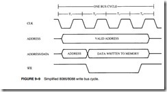
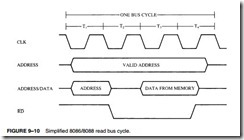
The three buses of the 8086 and 8088—address, data, and control—function exactly the same way as those of any other microprocessor. If data are written to the memory (see the simplified timing for write in Figure 9–9), the microprocessor outputs the memory address on the address bus, out- puts the data to be written into memory on the data bus, and issues a write (WR) to memory and IO>M = 0 for the 8088 and M>IO = 1 for the 8086. If data are read from the memory (see the simplified timing for read in Figure 9–10), the microprocessor outputs the memory address on the address bus, issues a read memory signal (RD), and accepts the data via the data bus.

Timing in General

The 8086/8088 microprocessors use the memory and I/O in periods called bus cycles. Each bus cycle equals four system-clocking periods (T states). Newer microprocessors divide the bus cycle into as few as two clocking periods. If the clock is operated at 5 MHz (the basic operating frequency for these two microprocessors), one 8086/8088 bus cycle is complete in 800 ns. This means that the microprocessor reads or writes data between itself and memory or I/O at a maxi- mum rate of 1.25 million times a second. (Because of the internal queue, the 8086/8088 can exe- cute 2.5 million instructions per second [MIPS] in bursts.) Other available versions of these microprocessors operate at much higher transfer rates due to higher clock frequencies.

8086-8088 Hardware Specifications-00128086-8088 Hardware Specifications-0013

During the first clocking period in a bus cycle, which is called T1, many things happen. The address of the memory or I/O location is sent out via the address bus and the address/data bus connections. (The address/data bus is multiplexed and sometimes contains memory-addressing information, sometimes data.) During TI, control signals ALE, DT>R, and IO>M (8088) or M>IO (8086) are also output. The IO>M or M>IO signal indicates whether the address bus contains a memory address or an I/O device (port) number.

During T2, the 8086/8088 microprocessors issue the RD or WR signal, DEN, and in the case of a write, the data to be written appear on the data bus. These events cause the memory or I/O device to begin to perform a read or a write. The DEN signal turns on the data bus buffers, if they are present in the system, so the memory or I/O can receive data to be written, or so the microprocessor can accept the data read from the memory or I/O for a read operation. If this hap- pens to be a write bus cycle, the data are sent out to the memory or I/O through the data bus.

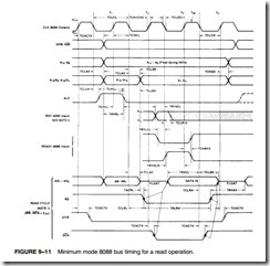
READY is sampled at the end of T2, as illustrated in Figure 9–11. If READY is low at this time, T3 becomes a wait state (Tw). (More detail is provided in Section 9–5.) This clocking period is provided to allow the memory time to access data. If the bus cycle happens to be a read bus cycle, the data bus is sampled at the end of T3.

In T4, all bus signals are deactivated in preparation for the next bus cycle. This is also the time when the 8086/8088 samples the data bus connections for data that are read from memory or I/O. In addition, at this point, the trailing edge of the WR signal transfers data to the memory or I/O, which activates and writes when the WR signal returns to a logic 1 level.

Read Timing

Figure 9–11 also depicts the read timing for the 8088 microprocessor. The 8086 read timing is identical except that the 8086 has 16 rather than eight data bus bits. A close look at this timing diagram should allow you to identify all the main events described for each T state.

The most important item contained in the read timing diagram is the amount of time allowed for the memory or I/O to read the data. Memory is chosen by its access time, which is the fixed amount of time that the microprocessor allows it to access data for the read operation. It is therefore extremely important that the memory chosen complies with the limitations of the system.

The microprocessor timing diagram does not provide a listing for memory access time. Instead, it is necessary to combine several times to arrive at the access time. To find memory

8086-8088 Hardware Specifications-0014

access time in this diagram, first locate the point in T3 when data are sampled. If you examine the timing diagram closely, you will notice a line that extends from the end of T3 down to the data bus. At the end of T3, the microprocessor samples the data bus.

Memory access time starts when the address appears on the memory address bus and continues until the microprocessor samples the memory data at T3. Approximately three T states elapse between these times. (See Figure 9–12 for the following times.) The address does not appear until TCLAV time (110 ns if the clock is 5 MHz) after the start of T1. This means that TCLAV time must be subtracted from the three clocking states (600 ns) that separate the appearance of the address (T1) and the sampling of the data (T3). One other time must also be subtracted: the data setup time (TDVCL), which occurs before T3. Memory access time is thus three clocking states minus the sum of TCLAV and TDVCL. Because TDVCL is 30 ns with a 5 MHz clock, the allowed memory access time is only 460 ns (access time = 600 ns – 110 ns – 30 ns).

The memory devices chosen for connection to the 8086/8088 operating at 5 MHz must be able to access data in less than 460 ns, because of the time delay introduced by the address decoders and buffers in the system. At least a 30- or 40-ns margin should exist for the operation of these circuits. Therefore, the memory speed should be no slower than about 420 ns to operate correctly with the 8086/8088 microprocessors.

8086-8088 Hardware Specifications-0015

The only other timing factor that may affect memory operation is the width of the RD strobe. On the timing diagram, the read strobe is given as TRLRH. The time for this strobe is 325 ns (5 MHz clock rate), which is wide enough for almost all memory devices manufactured with an access time of 400 ns or less.

Write Timing

Figure 9–13 illustrates the write-timing diagram for the 8088 microprocessor. (Again, the 8086 is nearly identical, so it need not be presented here in a separate timing diagram.)

The main differences between read and write timing are minimal. The RD strobe is replaced by the WR strobe, the data bus contains information for the memory rather than information from the memory, and DT>R remains a logic 1 instead of a logic 0 throughout the bus cycle.

When interfacing some memory devices, timing may be especially critical between the point at which WR becomes a logic 1 and the time when the data are removed from the data bus. This is the case because, as you will recall, memory data are written at the trailing edge of the WR strobe. According to the timing diagram, this critical period is TWHDX or 88 ns when the 8088 is operated with a 5 MHz clock. Hold time is often much less than this; it is, in fact, often 0 ns clip_image013[2]for memory devices. The width of the WR strobe is TWLWH or 340 ns at a 5 MHz clock rate. This rate is compatible with most memory devices that have an access time of 400 ns or less.

8086-8088 Hardware Specifications-0016