BUS TIMING
It is essential to understand system bus timing before choosing a memory or I/O device for inter- facing to the 8086 or 8088 microprocessors. This section provides insight into the operation of the bus signals and the basic read and write timing of the 8086/8088. It is important to note that we discuss only the times that affect memory and I/O interfacing in this section.
Basic Bus Operation
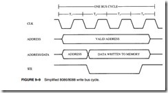
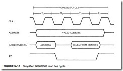
The three buses of the 8086 and 8088—address, data, and control—function exactly the same way as those of any other microprocessor. If data are written to the memory (see the simplified timing for write in Figure 9–9), the microprocessor outputs the memory address on the address bus, out- puts the data to be written into memory on the data bus, and issues a write (WR) to memory and IO>M = 0 for the 8088 and M>IO = 1 for the 8086. If data are read from the memory (see the simplified timing for read in Figure 9–10), the microprocessor outputs the memory address on the address bus, issues a read memory signal (RD), and accepts the data via the data bus.
Timing in General
The 8086/8088 microprocessors use the memory and I/O in periods called bus cycles. Each bus cycle equals four system-clocking periods (T states). Newer microprocessors divide the bus cycle into as few as two clocking periods. If the clock is operated at 5 MHz (the basic operating frequency for these two microprocessors), one 8086/8088 bus cycle is complete in 800 ns. This means that the microprocessor reads or writes data between itself and memory or I/O at a maxi- mum rate of 1.25 million times a second. (Because of the internal queue, the 8086/8088 can exe- cute 2.5 million instructions per second [MIPS] in bursts.) Other available versions of these microprocessors operate at much higher transfer rates due to higher clock frequencies.
During the first clocking period in a bus cycle, which is called T1, many things happen. The address of the memory or I/O location is sent out via the address bus and the address/data bus connections. (The address/data bus is multiplexed and sometimes contains memory-addressing information, sometimes data.) During TI, control signals ALE, DT>R, and IO>M (8088) or M>IO (8086) are also output. The IO>M or M>IO signal indicates whether the address bus contains a memory address or an I/O device (port) number.
During T2, the 8086/8088 microprocessors issue the RD or WR signal, DEN, and in the case of a write, the data to be written appear on the data bus. These events cause the memory or I/O device to begin to perform a read or a write. The DEN signal turns on the data bus buffers, if they are present in the system, so the memory or I/O can receive data to be written, or so the microprocessor can accept the data read from the memory or I/O for a read operation. If this hap- pens to be a write bus cycle, the data are sent out to the memory or I/O through the data bus.
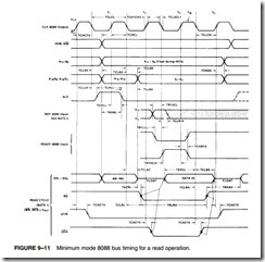
READY is sampled at the end of T2, as illustrated in Figure 9–11. If READY is low at this time, T3 becomes a wait state (Tw). (More detail is provided in Section 9–5.) This clocking period is provided to allow the memory time to access data. If the bus cycle happens to be a read bus cycle, the data bus is sampled at the end of T3.
In T4, all bus signals are deactivated in preparation for the next bus cycle. This is also the time when the 8086/8088 samples the data bus connections for data that are read from memory or I/O. In addition, at this point, the trailing edge of the WR signal transfers data to the memory or I/O, which activates and writes when the WR signal returns to a logic 1 level.
Read Timing
Figure 9–11 also depicts the read timing for the 8088 microprocessor. The 8086 read timing is identical except that the 8086 has 16 rather than eight data bus bits. A close look at this timing diagram should allow you to identify all the main events described for each T state.
The most important item contained in the read timing diagram is the amount of time allowed for the memory or I/O to read the data. Memory is chosen by its access time, which is the fixed amount of time that the microprocessor allows it to access data for the read operation. It is therefore extremely important that the memory chosen complies with the limitations of the system.
The microprocessor timing diagram does not provide a listing for memory access time. Instead, it is necessary to combine several times to arrive at the access time. To find memory
access time in this diagram, first locate the point in T3 when data are sampled. If you examine the timing diagram closely, you will notice a line that extends from the end of T3 down to the data bus. At the end of T3, the microprocessor samples the data bus.
Memory access time starts when the address appears on the memory address bus and continues until the microprocessor samples the memory data at T3. Approximately three T states elapse between these times. (See Figure 9–12 for the following times.) The address does not appear until TCLAV time (110 ns if the clock is 5 MHz) after the start of T1. This means that TCLAV time must be subtracted from the three clocking states (600 ns) that separate the appearance of the address (T1) and the sampling of the data (T3). One other time must also be subtracted: the data setup time (TDVCL), which occurs before T3. Memory access time is thus three clocking states minus the sum of TCLAV and TDVCL. Because TDVCL is 30 ns with a 5 MHz clock, the allowed memory access time is only 460 ns (access time = 600 ns – 110 ns – 30 ns).
The memory devices chosen for connection to the 8086/8088 operating at 5 MHz must be able to access data in less than 460 ns, because of the time delay introduced by the address decoders and buffers in the system. At least a 30- or 40-ns margin should exist for the operation of these circuits. Therefore, the memory speed should be no slower than about 420 ns to operate correctly with the 8086/8088 microprocessors.
The only other timing factor that may affect memory operation is the width of the RD strobe. On the timing diagram, the read strobe is given as TRLRH. The time for this strobe is 325 ns (5 MHz clock rate), which is wide enough for almost all memory devices manufactured with an access time of 400 ns or less.
Write Timing
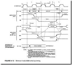
Figure 9–13 illustrates the write-timing diagram for the 8088 microprocessor. (Again, the 8086 is nearly identical, so it need not be presented here in a separate timing diagram.)
The main differences between read and write timing are minimal. The RD strobe is replaced by the WR strobe, the data bus contains information for the memory rather than information from the memory, and DT>R remains a logic 1 instead of a logic 0 throughout the bus cycle.
When interfacing some memory devices, timing may be especially critical between the point at which WR becomes a logic 1 and the time when the data are removed from the data bus. This is the case because, as you will recall, memory data are written at the trailing edge of the WR strobe. According to the timing diagram, this critical period is TWHDX or 88 ns when the 8088 is operated with a 5 MHz clock. Hold time is often much less than this; it is, in fact, often 0 ns ![]() for memory devices. The width of the WR strobe is TWLWH or 340 ns at a 5 MHz clock rate. This rate is compatible with most memory devices that have an access time of 400 ns or less.
for memory devices. The width of the WR strobe is TWLWH or 340 ns at a 5 MHz clock rate. This rate is compatible with most memory devices that have an access time of 400 ns or less.


