Switch interfaces:Multi-state switch

Multi-state switch

Context

● You are developing an embedded application using one or more members of the 8051 family of microcontrollers.

● The application has a time-triggered architecture, constructed using a scheduler.

● You are creating the user interface for your application.

Problem

How do you obtain the behaviour illustrated in Figure 19.13 from a single, push- button switch connected to the port pin of a microcontroller?

image

Background

Solution

Although – as discussed in ON OFF SWITCH [page 414] – sustained switch depressions can sometimes be problematic, they can also form the basis of more complex switch- based interfaces and can allow us to turn this two-state input device into a three-state (or more) input device.

For example, if we have a real-time clock, we may have just two buttons (‘forward’ and ‘backward’) to set the time. To avoid this process becoming unduly tedious, we might decide that a brief depression of the ‘Forward’ button should slowly increment the displayed time, while a sustained depression (longer than, say, five seconds), should advance the display more rapidly.

To implement this type of behaviour, we might operate as follows:

● We keep track of the period of time over which the switch has been continually depressed.

● When the depression exceeds a threshold (call it Duration A), we treat this like a normal switch depression.

● When the depression exceeds a larger threshold (call it Duration B), we treat this as a sustained switch depression.

Note that further ‘levels’ can be added, but more than two (sometimes three) can be confusing to the user.

See the example that follows for complete implementation details.

Hardware resource implications

Creating a multi-state switch imposes very minor loads on CPU and memory resources.

Reliability and safety issues

The use of multi-state switches does not generally have reliability or safety implications.

Refer to SWITCH INTERF ACE ( SOFTW ARE ) [page 399] and SWITCH INTERF ACE

( HARDW ARE ) [page 410] for general discussions about the safety of switch interfaces.

Portability

This pattern may be adapted for use with other microcontrollers without difficulty.

Overall strengths and weaknesses

A cost-effective way of improving the usability of many applications.

Related patterns and alternative solutions

See ON OFF SWITCH [page 414].

Example: Counter

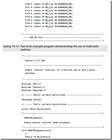
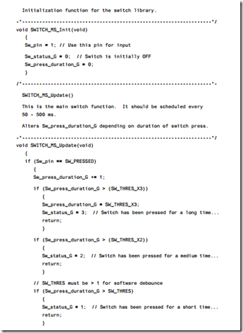
In this example, we demonstrate the key features of a multi-state switch by means of a counter that is incremented at a rate which depends on the switch-press duration (Listings 19.10 to 19.14).

The required hardware is illustrated in Figure 19.14.

image

image

image

image

image

image

image

image


Switch interfaces:On-off switch

Onoff switch

Context

● You are developing an embedded application using one or more members of the 8051 family of microcontrollers.

● The application has a time-triggered architecture, constructed using a scheduler.

● You are creating the user interface for your application.

Problem

How do you obtain the behaviour illustrated in Figure 19.9 from a single, push- button switch connected to the port pin of a microcontroller?

image

The switch is intended to operate as follows:

● The user presses the switch to turn on a piece of equipment.

● The equipment operates as required.

● The user presses the switch again to turn off the equipment.

This seems very straightforward. However, suppose we are applying the basic approach to switch reading presented in SWITCH INTERF ACE ( SOFTW ARE ) [page 399], or SWITCH INTERF ACE ( HARDW ARE ) [page 410]. This can be summarized as follows:

1 We read the relevant port pin.

2 If we think we have detected a switch depression, we read the pin again 100 ms later.

3 If the second reading confirms the first reading, we assume the switch really has been depressed.

This is what can happen:

● The user presses the switch to turn on the piece of equipment.

● The switch is checked. It is depressed.

● The switch is checked (say) 100 ms later: the second check confirms the first. The equipment is turned on.

● The switch is checked 100 ms later. It is still depressed.

● The switch is checked 100 ms later: the second check confirms the first. The equip- ment is turned off again.

● And so on.

This behaviour arises because the user will generally wait until the equipment begins to work and will then remove their finger from the switch. In the best case sce- nario, a switch depression is likely to last about 500 ms. Unless we take action to prevent it, the equipment will ‘flicker’ on and off.

Solution

We can most simply create an on-off switch by adding a ‘switch block’ counter to the existing interface code. This works as follows:

1 Every time we find the switch has been pressed, we ‘block’ it for – say – 1 second.

2 While the switch is blocked, any changes in switch status are ignored: thus, for example, if the user keeps the switch depressed for half a second, this fact will be ignored.

The ‘on-off’ example that follows illustrates how this is achieved in practice.

Hardware resource implications

Reading a switch input imposes minimal loads on CPU and memory resources.

Reliability and safety issues

In hostile environments, this code should be based on SWITCH INTERF ACE ( HARD W ARE ) [page 410].

Note that, where safety is a primary concern, the blocking of switch inputs may not be appropriate. As an alternative, you can retain the basic switch-handling approach, but use two switches (Figure 19.11).

The use of two switches can make it easier to react quickly to changes in the inputs and may be safer under some circumstances.

image

Portability

This pattern may be adapted for use with other microcontrollers without difficulty.

Overall strengths and weaknesses

A simple way of achieving ‘ON–OFF’ behaviour from a single switch.

Related patterns and alternative solutions

This pattern builds on SWITCH INTERF ACE ( SOFTW ARE ) [page 399] and / or SWITCH INTERF ACE ( HARDW ARE ) [page 410].

See ‘Reliability and safety issues’ for an alternative solution.

Example: Controlling a flashing LED

In this example, we use the hardware in Figure 19.12 to illustrate the creation of an on-off switch interface.

The key software files required in this example are presented in Listings 19.6 to 19.9: as usual, a complete set of files for the project are included on the CD.

image

image

image

image

image

image


Switch interfaces:Switch interface (software)

Switch interface (software)

Context

● You are developing an embedded application using one or more members of the 8051 family of microcontrollers.

● The application has a time-triggered architecture, constructed using a scheduler.

● You are creating the user interface for your application.

Problem

How do you connect the port pin of an 8051 microcontroller to some form of mechanical switch (for example, a simple push-button switch or an electromechani- cal relay)?

Background

Consider the simple push-button switches illustrated in Figure 19.1.

Depressing this switch will, in either arrangement, cause a voltage change from approximately Vcc to 0V at the input port.

In an ideal world, this change in voltage would take the form illustrated in Figure 19.2 (top). In practice, all mechanical switch contacts bounce (that is, turn on and off, repeatedly, for a short period of time) after the switch is closed or opened. As a result, the actual input waveform looks more like that shown in Figure 19.2 (bottom). Usually, switches bounce for less than 20 ms: however large mechanical switches

image

image

exhibit bounce behaviour for 50 ms or more.

This bounce is equivalent to pressing an idealized switch multiple times. This causes various potential problems, not least:

● If we need to distinguish between single and multiple switch presses: for example, rather than reading ‘A’ from a keypad, we read ‘AAAAA’.

● If we wish to count the number of switch presses.

● If we need to distinguish between a switch being depressed and being released: for example, if the switch is depressed once and then released some time later, the bounce will make it appear as if the switch has been pressed again.

Solution

Checking for a switch input is, in essence, straightforward:

1 We read the relevant port pin.

2 If we think we have detected a switch depression, we read the pin again (say) 20 ms later.

3 If the second reading confirms the first reading, then we assume the switch really has been depressed.

Note that the figure of ‘20 ms’ will, of course, depend on the switch used: the data sheet of the switch will provide this information. If you have no data sheet, you can either experiment with different figures or measure directly using an oscilloscope.

We illustrate this basic procedure in the example.

Hardware resource implications

Reading a switch input in software imposes very minor loads on CPU and memory resources.

Reliability and safety issues

We consider some reliability and safety issues associated with switches here.

Latching vs. push-button switches

All the examples in this chapter (and throughout this book) focus on the use of push- button (rather than ‘latching’) switches.

To illustrate why this is the case, we will consider two possible designs for a switch- based interface (Figure 19.3). The first interface design uses a ‘latching’ switch: specifically, this is a 5-position, rotary switch. The second design uses two push- button switches and five LEDs to provide similar functionality.

We can immediately see some advantages of the push-button solution when we consider how each system behaves when power is first applied and in an emergency situation.

In the case of the push-button solution, the software designer has control of the initial state. For example, if it is appropriate to always start the system in ‘State 2’ (as illustrated in Figure 19.3), this can be easily achieved. Similarly, suppose that State 5 involves control of a piece of machinery: if a problem develops with the machine, we might need to change the system to (say) State 4. Again, we can do this under soft- ware control and we can make this change clear to the user simply by lighting the appropriate LED.

The rotary switch interface behaves very differently. If the user moves the switch to Position 5 before applying power, then, at power up, how do we move the system to State 2? And if we do change the state to State 2, we cannot indicate this fact to the user, since we are unable to move the rotary switch. Similarly, in the emergency situa- tion just discussed, we may be able to shut down the machine under software control, but we cannot show the user that the system is now in State 4.

image

These problems arise not just with multi-state rotary switches but with any form of latching switch.

We can summarize the advantage of the push-button solution by saying that it leaves the software in control of the hardware, rather than vice versa. This is a good general design guideline in embedded systems.

Switch bounce times

In electrical engineering terms, the switches used as inputs in a typical microcontroller system are ‘dry’. This means that, because they must handle only small currents (< 20 mA) and voltages (< 10V), they suffer little (electrical) ‘wear and tear’ and can be expected to have a long life.

However, switches also have moving mechanical parts and their performance, inevitably, varies with age. Even a good quality switch will change its performance as it is used: in particular, the period of bounce tends to increase with age. As a result, it is important not to trust to luck or experiments with new switches when determining appropriate debounce times: you should allow a margin (at least 20%) with new switches to allow for the impact of prolonged usage.

Using single-pole switches

We have already discussed the advantages of push-button (PB) switches. Unfortunately, simply using a PB switch is not enough to ensure reliability. For exam- ple, consider again the switch in Figure 19.1: this type of switch is often referred to as ‘normally open’ (NO). If this form of NO switch is removed or damaged, leaving the connection permanently open, we cannot detect this fact in software. This may have safety or reliability implications.

In some circumstances, there may be advantages to using a ‘normally closed’ (NC) PB switch (Figure 19.4). Using a PB-NC switch, we can detect the removal of the switch or damage to the wiring, although we cannot generally distinguish this from a normal (sustained) switch depression.

image

We can provide an even more reliable solution by using a PB ‘double-pole, double- throw’ (PB-DPDT) switch (Figure 19.5). This generates two inputs, which will always have opposite logic if the switch is undamaged and wired correctly. Using such an input device, we can detect various types of switch faults (including switch removal) and wiring faults (including wire cutting).

Note that such a switch requires two input pins and slightly more software than a single-pole switch input.

image

Out-of-range inputs and ESD

Like all software-only input techniques, SWITCH INTERF ACE ( SOFTW ARE ) provides no protection against out-of-range inputs: if someone applies +/–20V to your switch (by mistake or deliberately), they may ‘fry’ the microcontroller.

Similar problems arise in the event of electrostatic discharge (ESD). ESD can present a significant problem in harsh environments (e.g. industrial systems, automotive applications) and compliance with international standards in this area (e.g. IEC 1000- 4-2) is a requirement for some applications.

There is little you can do, in software, to guard again either of these situations. See

SWITCH INTERF ACE (HARDW ARE ) [page 410] for a discussion of this issue and a solution.

Portability

None of these discussions in this pattern is 8051 specific: the pattern may be used with other microcontroller families without difficulty.

Overall strengths and weaknesses

SWITCH INTERF ACE ( SOFTW ARE ) requires a minimum of external hardware.

It is very flexible: for example, the programmer can incorporate ‘auto-repeat’ functions with few code changes.

It is simple and cheap to implement.

Like all software-only input techniques, SWITCH INTERF ACE ( SOFTW ARE ) pro- vides no protection against out-of-range inputs or electrostatic discharge (ESD). See SWITCH INTERF ACE ( HARDW ARE ) [page 410] for a discussion of this issue and a solution.

Related patterns and alternative solutions

Reading a switch input is a classic example of a situation where we can trade hard- ware cost against software complexity. For an alternative approach using hardware, consider SWITCH INTERF ACE ( HARDW ARE ) [page 410].

Where the switch (or other input device) does not suffer from bounce (for exam- ple, where your input is derived from a solid-state relay or some other form of ‘electronic switch’) then much of the complexity of these input strategies can be avoided through the use of PORT I / O [page 174].

Example: Controlling a flashing LED

In this example, we use a push-button switch to control the flashing of an LED. Here the LED flashes only when the switch is pressed.

The hardware used is illustrated in Figure 19.6 and the software framework is given in Listings 19.1 to 19.4.

image

image

image

image

image

image


Keypad interfaces:Keypad interface

Keypad interface

Context

● You are developing an embedded application using one or more members of the 8051 family of microcontrollers.

● The application has a time-triggered architecture, constructed using a scheduler.

● You are creating the user interface for your application.

Problem

How do you connect a small keypad, similar to that illustrated in Figure 20.1, to your application?

image

Background

See Chapter 19 for background information on the reading of single switches.

Solution

Basics

We are concerned here with keypads made up of a matrix of switches, in an arrange- ment similar to that illustrated in Figure 20.2.

Some key points to note are as follows:

● The matrix arrangement is used to save port pins. If we have R rows and C columns of keys, we need R + C pins if we use a matrix arrangement and R × C pins if we use individual switches. If you need six or more keys, then the matrix arrangement requires fewer pins.

image

[Note: The pull-up resistors may be omitted, as usual, if the port has internal pull-ups.]

Many keypads have 12 keys (‘0’–‘9’ plus two function keys – typically ‘#’ and ‘*’). Using a matrix arrangement, this requires seven port pins.

● The keys may bounce, when pressed and released.

● The duration of the key press will generally be at least 500 ms.

● The keys will not generally be allowed to ‘auto repeat’: this can be very confusing for users.

● We may wish the user to be able to press one or more ‘function keys’ in combina- tion with other keys.

Keypad scanning

At the heart of any keypad code is a scanning function: this will typically go through each column in turn and identify if any key in that column has been pressed.

Consider, for example, the keypad shown in Figure 20.3.

In Figure 20.3, the numbers adjacent to the rows and column indicate the port pins to which the keypad should be connected. Pins 0, 1 and 2 (the columns) will be referred to here as the output pins: these are written to during the scanning process. Pins 3, 4, 5 and 6 will be referred to as the input pins: these are read during the scan- ning process.

image

Suppose we wish to see if the key ‘1’ is pressed. We can proceed as follows:

● We set the corresponding output pin (in this case, Pin 6) to a Logic 0 value and the remaining output pins to a Logic 1 value.

● We read the required input pin (in this case, Pin 0).

If this pin is a Logic 1, then the key ‘1’ is not pressed: the Logic 1 value is, instead, obtained via the pull-up resistor on the port pin.

If this pin is at Logic 0, then the key is being pressed (subject to debounce con- siderations): the Logic 0 voltage reading results from the Logic 0 voltage output on Pin 6.

● We must repeat the reading (say) 200 ms later, to allow for switch bounce.

We need to repeat this process for every key. Listing 20.1 illustrates one way of per- forming this scanning for the whole keypad.

image

image

image

Function keys

Note that more than one key may be pressed at the same time. The ‘function keys’ (‘#’ and ‘*’) in Listing 20.1 illustrate how we can make use of multiple key depressions.

The main code example presented with this pattern illustrate the use of function keys.

Buffer arrangements

In most scheduled keypad routines, it is useful to have a small buffer, so that key presses are not lost if the system is unable to process them immediately.

Numerous buffer arrangements are possible: the main code example presented with this pattern illustrates one possibility.


Switch interfaces:Switch interface (hardware)

Switch interface (hardware)

Context

● You are developing an embedded application using one or more members of the 8051 family of microcontrollers.

● The application has a time-triggered architecture, constructed using a scheduler.

● You are creating the user interface for your application.

Problem

How do you create a very robust switch interface for use in a hostile (e.g. industrial, automotive) environment?

Background

Consider the following scenarios:

● Your embedded application is used in an industrial environment where high levels of electrostatic discharge are likely. How can you ensure that your device remains fully operational?

● Your automotive security application may be the subject of deliberate vandalism or damage. Specifically, reports on the WWW have revealed that thieves have found it possible to disable a similar security system by applying 12V from a car battery directly to one of the system switches. How can you ensure that your system is more robust?

In general, SWITCH INTERF ACE ( SOFTW ARE ) [page 399] describes techniques that are only suitable in ‘safe’ applications: in hostile environments, you need a more robust solution. This must be hardware based.

Solution

As noted in ‘Background’, creating a robust switch interface requires the use of off- chip hardware.

Traditionally, techniques involving J-K flip-flops, high-impedence CMOS gates or R-C integrators have all been used for switch debouncing: Huang (2000), for example, provides details of these techniques. In general, these approaches – while performing the debounce operation – provide only very limited protection, at best, again ESD and similar hazards. Because, as we saw in SWITCH INTERF ACE ( SOFTW ARE ) [page 399], the process of switch debouncing is almost trivial in a scheduled application, the cost of external hardware for switch debouncing alone cannot generally be justified.

More recently, several specialized ICs for protection and switch debouncing have appeared on the market. Of these, the Maxim 6816/6817/6818 family are a good example (Figure 19.7).

This is how Maxim describes these devices:

● The Max6816/Max6817/Max6818 are single, dual, and octal switch debouncers that provide clean interfacing of mechanical switches to digital systems. They accept one or more bouncing inputs from a mechanical switch and produce a clean digital output after a short, preset qualification delay. Both the switch opening bounce and the switch closing bounce are removed.

● Robust inputs can exceed power supplies by up to ±25V.

● ESD protection for input pins:

±15 kV Human Body Model

±8 kV IEC 1000-4-2, Contact Discharge

±15 kV IEC 1000-4-2, Air-Gap Discharge

● Single-supply operation from +2.7V to +5.5V.

● Single (Max6816), dual (Max6817) and octal (Max6818) versions available.

● No external components required.

● 6 µA supply current.

image

Hardware resource implications

Reading a debounced switch input imposes minimal loads on CPU and memory resources.

Reliability and safety issues

For the reasons discussed in ‘Solution’, this is a highly reliable method for creating a switch interface.

For additional reliability – particularly in the event of malicious damage – see SWITCH INTERF ACE ( SOFTW ARE ) [page 399] for discussions on the use of multi-pole switches.

Portability

These techniques are inherently portable.

Overall strengths and weaknesses

Greatly increased reliability (compared with software-only solutions) in hostile environments.

Increased costs and hardware complexity.

Related patterns and alternative solutions

See SWITCH INTERF ACE ( SOFTW ARE ) [page 399].

Example: Reading 8 switch inputs in a hostile environment

Figure 19.8 illustrates the use of a Max6818 to read the inputs from eight switches connected to Port 1 of an 8051 device. The results are reported on Port 2.

image

image


Example: An output-only library for the 8051/8052 (generic)

Example: An output-only library for the 8051/8052 (generic)

This example again illustrates how to link a Standard 8051 device to a PC.

Unlike the first example, the software is ‘write only’: data are transferred from the microcontroller to the PC but not vice versa. To illustrate this, the software displays elapsed time on the PC via a terminal emulator program.

In Figure 18.6, we illustrate this software running on the Keil hardware simulator. Of course, it may equally well display its outputs using Hyperterminal (or equivalent), as in Figure 18.3: however, the use of the hardware simulator is useful during the early stages of program development.

The hardware shown in Figure 18.2 can again be used here to run this program. The source code for this example is included on the CD.

image

Further reading

In a very readable book, Axelson (1998) considers the use of RS-232 communications. Although she discusses 8051 microcontrollers, the main focus is on the PC end of the communication link. Axelson provides some useful code examples that can be adapted for use in many PC-based data acquisition and monitoring systems.


Switch interfaces

Introduction

Reading the status of one or more push-button switches is a very common require- ment in embedded applications. The four patterns in this chapter describe different solutions to this problem.

The patterns are as follows:

SWITCH INTERF ACE ( SOFTW ARE ) [page 399]

Uses a minimum of external hardware. Reads a single switch, debounces it and reports its status

SWITCH INTERF ACE ( HARDW ARE ) [page 410]

Use external hardware to perform switch debouncing. Increased cost (compared with SWITCH INTERF ACE ( SOFTW ARE ) ), but much higher level of protection against ESD, malicious damage etc.

ON OFF SWITCH [page 414]

Building on SWITCH INTERF ACE ( SOFTW ARE ) or SWITCH INTERF ACE ( HARD

W ARE ) this pattern provides, through software, the following behaviour:

Assume that the switch is in the OFF state. It remains in this state until it is pressed. When pressed, the state changes to ON. It remains in this state until it is pressed. When pressed, the state changes to OFF.

This type of behaviour can be used, for example, to allow a single (non-latching) switch to control a piece of machinery.

MUL TI ST A TE SWITCH [page 423]

Building on SWITCH INTERF ACE ( SOFTW ARE ) or SWITCH INTERF ACE ( HARD

W ARE ) this pattern provides, through software, the following behaviour:

Assume that the switch state is in the OFF state. The switch is pressed and briefly held. The switch state changes to ‘ON STATE 1’. The user continues to depress the switch. The switch state becomes ‘ON STATE 2’, etc. Releasing the switch (at any time) puts the switch back in the OFF state.

That is, the switch state depends on the duration of the switch press. Any number of ‘ON’ states may be supported (although having more than around three is generally very confusing for the user).

This type of behaviour can be useful when, for example, setting time on a clock. Pressing the set switch will initially cause the displayed time to change slowly; sus- tained depressions will cause the displayed time to increase more rapidly.

Note: For reasons discussed in SWITCH INTERF ACE ( SOFTW ARE ) , in ‘Safety and reliability’, we are only concerned with push-button switches in these patterns: ‘toggle’ or ‘latching’ switches are not considered (and the use of such switches is not recommended).


Communicating with PCs via RS-232:Pc link (rs-232)

Pc link (rs-232)

Context

● You are developing an embedded application using one or more members of the 8051 family of microcontrollers.

● The application has a time-triggered architecture, constructed using a scheduler.

● You are creating the user interface for your application.

Problem

How do you link your embedded application to a desktop (or notebook or hand-held) PC using ‘RS-232’?

Background

This pattern is concerned with the use of what is commonly referred to as the RS-232 communication protocol, to transfer data between an 8051 microcontroller and some form of personal computer (PC, notebook or similar).

We provide some important background information on RS-232 in this section. We begin, however, by considering some important terminology used in the communica- tions area.

What are ‘simplex’, ‘half-duplex’ and ‘duplex’ serial communications?

In a simplex serial communication system, we typically require at least two wires (’signal’ and ‘ground’). Data transfer is only in one direction: for example, we might transfer data from a simple data-monitoring system to a PC using simplex data transfer.

In a half-duplex serial communication system we again (typically) require at least two wires. Here, data transfer can be in both directions. However, transmission can only be in one direction at a time. In a variation of the data-monitoring example, we might use a half-duplex communication strategy to allow us to send information to the embedded module (to set parameters, such as sampling rate). We might also, at other times, use the same link to download the data from the embedded board to a PC. In a full-duplex serial communication system, we typically require at least three wires (Signal A, Signal B, Ground). The line Signal A will carry data in one direction at

the same time that Signal B carries data in the other direction.

What is ‘RS-232’?

In 1997 the Telecommunications Industry Association released what is formally known as TIA-232 Version F, a serial communication protocol which has been

universally referred to as ‘RS-232’ since its first ‘Recommended Standard’ appeared in the 1960s. Similar standards (V.28) are published by the International Telecommunications Union (ITU) and by CCITT (Consultative Committee International Telegraph and Telephone).

The ‘RS-232’ standard includes details of:

● The protocol to be used for data transmission.

● The voltages to be used on the signal lines.

● The connectors to be used to link equipment together.

Overall, the standard is comprehensive and widely used, at data transfer rates of up to around 115 or 330 kbits / second (115 / 330 k baud). Data transfer can be over distances of 15 metres or more.

Note that RS-232 is a peer-to-peer communication standard. Unlike the multi-drop RS-485 standard (which we consider in Chapter 27), RS-232 is intended to link only two devices together.

Basic RS-232 protocol

RS-232 is a character-oriented protocol. That is, it is intended to be used to send single 8-bit blocks of data. To transmit a byte of data over an RS-232 link, we gener- ally encode the information as follows:

● We send a ‘Start’ bit.

● We send the data (8 bits).

● We send a ‘Stop’ bit (or bits).

We consider each of these stages here.

Quiescent state

When no data are being sent on an RS-232 ‘transmit’ line, the line is held at a Logic 1 level.

Start bit

To indicate the start of a data transmission we pull the ‘transmit’ line low.

Data

Data are often encoded in ASCII (American Standard Code for Information Interchange), in 7-bit form. The bits are sent least significant bit first. If we are send- ing 7-bit data, the eighth data bit is often used as a simple parity check bit and is transmitted in order to provide a rudimentary error detection facility on a character- by-character basis.

Note that none of the code presented here uses parity bits: we use all 8 bits for data transfer.

Stop bit(s)

The stop bits consist of a Logic 1 output. These can be 1 or, less commonly, 1G or 2 pulses wide.

Note that we will use a single stop bit in all code example.

Asynchronous data transmission and baud rates

RS-232 uses an asynchronous protocol. This means that no clock signal is sent with the data. Instead, both ends of the communication link have an internal clock, run- ning at the same rate. The data (in the case of RS-232, the ‘Start’ bit) is then used to synchronize the clocks, if necessary, to ensure successful data transfer.

RS-232 generally operates at one of a (restricted) range of baud rates. Typically these are: 75, 110, 300, 1,200, 2,400, 4,800, 9,600, 14,400, 19,200, 28,800, 33,600,

56,000, 115,000 and (rarely) 330,000 baud. Of these, 9,600 baud is a very ‘safe’ choice, as it is very widely supported.

RS-232 voltage levels

The threshold levels used by the receiver are +3V and -3V and the lines are inverted. The maximum voltage allowed is +/- 15V.

Note that these voltages cannot be obtained directly from the naked microcon- troller port pins: some form of interface hardware is required. For example, the Maxim Max232 and Max233 are popular and widely used line driver chips; we con- sider how to use such chips in ‘Solution’.

Flow control

RS-232 is often used with some form of flow control. This is a protocol, implemented through software or hardware, that allows a receiver of data to tell the transmitter to pause the dataflow. This might be necessary, for example, if we were sending data to a PC and the PC had filled a RAM buffer: the PC would then tell our embedded applica- tion to pause the data transfer until the buffer contents had been stored on disk.

Although hardware handshaking can be used, this requires extra signal lines. The most common flow control technique is ‘Xon / Xoff’ control. This requires a half- or full-duplex communication link, and can operate as follows:

1 Transmitter sends a byte of data.

2 The receiver is able to receive more data: it does nothing.

3 The transmitter sends another byte of data.

4 Steps 1–3 continue until the receiver cannot accept any more data: it then sends a ‘Control s’ (Xoff) character back to the transmitter.

5 The transmitter receives the ‘Xoff’ command and pauses the data transmission.

6 When the receiver node is ready for more data, it sends a ‘Control q’ (Xon) charac- ter to the transmitter.

7 The transmitter resumes the data transmission.

8 The process continues from Step 1.

Solution

In this section we consider how to implement an RS-232 link from an embedded 8051 microcontroller to a PC.

Transceiver hardware

As noted in ‘Background’, the voltages used in RS-232 communications are incompat- ible with the voltages used on the microcontroller itself. Therefore, you will require some form of voltage level conversion circuitry between the microcontroller board and the PC cable.

Usually the most cost-effective way of achieving this is to use a ‘transceiver’ (transmitter-receiver) chip created for this purpose. Of these, the Max232 (from Maxim) is frequently used; however, in new designs the more recent Max233 is a better choice as it requires fewer external components.

The required link to a Max233 is illustrated in Figure 18.1, which also shows the standard connections (9-pin D-type socket: ‘DB-9’) used for most recent designs.

image

Cable connections

To connect to the PC using the software presented here, you need a 3-wire cable.

Use DB-9 socket (‘female’) connector at the PC end and DB-9 plug (‘male’) connec- tor at the microcontroller end.

The required cable connections are a ‘straight through’ cable as described in Table 18.1.

image

The software architecture

Suppose we wish to transfer data to a PC at a standard 9,600 baud rate; that is, 9,600 bits per second. As we discussed in ‘Background’, transmitting each byte of data, plus stop and start bits, involves the transmission of ten bits of information (assuming a single stop bit is used). As a result, each byte takes approximately 1 ms to transmit.

This has important implications in all applications, not least those using a sched- uler. If, for example, we wish to send this information to the PC:

Current core temperature is 36.678 degrees

then the task sending these 42 characters will take more than 40 milliseconds to complete. This will frequently be an unacceptably long duration.

The most obvious way of solving this problem is to increase the baud rate; how- ever, this is not always possible and it does not solve the underlying problem.

A better solution is to write all data to a buffer in the microcontroller. The contents of this buffer will then be sent – usually one byte at a time – to the PC, using a regu- lar, scheduled task.

This solution is used in the code libraries presented in the following sections and included on the accompanying CD. The architecture is a good example of a MUL TI ST AGE T ASK [page 317], and is frequently used in user-interface libraries: LCD CHARACTER P ANEL [page 467], for example, uses a very similar architecture.

Using the on-chip U(S)ART for RS-232 communications

Having decided on the basic architecture for the RS-232 library, we need to consider in more detail how the on-chip serial port is used.

This port is full duplex, meaning it can transmit and receive simultaneously. It is also receive buffered, meaning it can commence reception of a second byte before a previously received byte has been read from the receive register. (However, if the first byte still has not been read by the time reception of the second byte is complete, one of the bytes will be lost.)

The serial port can operate in four modes (one synchronous mode, three asynchro- nous modes). In this pattern, we are primarily interested in Mode 1. In this mode, 10 bits are transmitted (through TxD) or received (through RxD): a start bit (0), 8 data bits (lsb first), and a stop bit (1).

Note that the serial interface may also provide interrupt requests when transmis- sion or reception of a byte has been completed. However, for reasons discussed in Chapter 1, none of the code used in this pattern will generate interrupts.

Serial port registers

The serial port control and status register is the special function register SCON. This register contains the mode selection bits (and the serial port interrupt bits, TI and RI).

SBUF is the receive and transmit buffer of serial interface. Writing to SBUF loads the transmit register and initiates transmission. Reading out SBUF accesses a physi- cally separate receive register.

Baud rate generation

There are several different ways to generate the baud rate clock for the serial port depending on the mode in which it is operating.

As already noted, we are primarily concerned here with the use of the serial port in Mode 1. In this mode the baud rate is determined by the overflow rate of Timer 1 or Timer 2. For reasons discussed in Chapter 14, we assume that, if Timer 2 is available, it will usually be used to drive the scheduler. Therefore, we focus on the use of Timer 1 for baud rate generation.

The baud rate is determined by the Timer 1 overflow rate and the value of SMOD follows:

image

image

Thus, the required value of TH1 is 252.7447916667.

The nearest integer value is 253. This means that our actual baud rate will be approximately 10,417 baud – more than 8% higher than the required (9,600) rate.

Remember: This is an asynchronous protocol and relies for correct operation on the fact that both ends of the connection are working at the same baud rate. In practice, you can generally work with a difference in baud rates at both ends of the connection by up to 5%, but no more.

Despite the possible 5% margin, it is always good policy to get the baud rate as close as possible to the standard value because, in the field, there may be significant temperature variations between the oscillator in the PC and that in the embedded system. This will lead to a ‘drift’ in baud rates on PC and microcontroller, even if they were precisely the same to start with: as a result, if the baud rates were initially mismatched, then communication with the PC may fail completely during normal use. This type of ‘inexplicable fault’ has caused many developers sleepless nights (’I don’t understand it! It works fine in all the tests in the lab!’).

Note also that it is generally essential to use some form of crystal oscillator (rather than a ceramic resonator) when working with asynchronous serial links (such as RS-232, RS-485 or CAN): the ceramic resonator is not sufficiently stable for this purpose: see CR YST AL OSCILLA TOR [page 54] and CERAMIC RESONA TOR [page 64]for details.

Dealing with the 11.0592 MHz problem

In a scheduled application, using an 11.0592 MHz crystal oscillator is not ideal. 11.0592 MHz may translate into precise baud rates, but it is not ideal as a source of ‘ticks’ in the scheduler: in particular, it is impossible to produce precise 1 ms ticks from an 8051 device driven by an 11.0592 MHz crystal.

There are at least four solutions to this problem:

● The first solution is to use a 11.0592 MHz crystal and work with a 5 ms tick inter- val. Note that a 5 ms interval can be generated precisely at this crystal frequency, as demonstrated in the example on the CD.

● The second solution is to use Timer 2 to generate the baud rates. Timer 2 allows precise baud-rate generation at a wider range of oscillator frequencies than Timer 1; of course – in a single-processor system – this means that Timer 2 cannot simulta- neously be used to generate the scheduler ticks, and Timer 0 or Timer 1 will need to be used for this purpose.

● The third solution is to use the dedicated baud rate generator included on recent 8051 devices. These allow very standard baud rates to be generated even with – say

– 12 MHz crystals. In addition, use of a dedicated generator frees up the other timers for general-purpose use. Again, one of the libraries on the CD make use of internal baud rate generator.

● The fourth solution is to use two-microcontroller solution, and a shared-clock

scheduler. Figure 18.2 illustrates this approach.

image

PC software

We focus in this pattern on the software required on the microcontroller in order to transfer data to a PC. Clearly, however, we also need software on the PC itself.

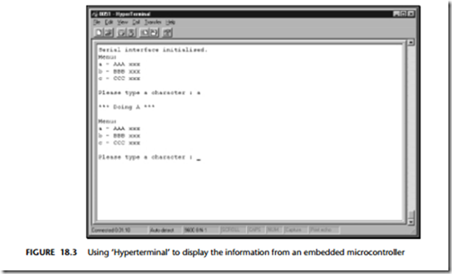
If your desktop computer is running Windows (95, 98, NT, 2000), then a simple but effective option is the ‘Hyperterminal’ application which is included with all of these operating systems. Figure 18.3 shows this application running one of the exam- ple applications.

While Hyperterminal (or similar terminal-emulator programs in other environ- ments) are useful, they are not suitable for all purposes.

If you need more specialized PC code for storing or analyzing data from your embedded application, you will probably need to write your own. Such programs lie beyond the scope of this book but Axelson (1998) is a good source of further informa- tion and useful code samples.
image

Hardware resource implications

The use of the PC link library described in this pattern has the following hardware resource implications:

● It uses the UART.

● It uses two port pins (P3.0, P3.1).

● It uses either a general-purpose timer or a specialized baud rate generator circuit.

Overall, however, it is the memory load that causes greatest difficulty, particularly in situations where only internal memory is available. The root of this difficulty is that fact that, as we discussed in ‘Solution’, the architecture used (to transmit data to the PC) is based on the use of a buffer to which the user writes as required; this buffer is then emptied, one character at a time, by a scheduled task.1

The buffer itself is very simple:

// The transmit buffer length

#define PC_LINK_TRAN_BUFFER_LENGTH 100

static tByte Tran_buffer[PC_LINK_TRAN_BUFFER_LENGTH];

If you run out of memory, there are several options:

● You can reduce the buffer size. This may mean that tasks in your applications must break down the data they send into smaller blocks. Typically, the main implication is that shorter strings must be used.

● You can increase the baud rate and adapt the code so that the scheduler sends more than one byte of data in every time the ‘update’ function is run.

● If using on-chip memory only, you can choose an 8051 device with additional on- chip RAM: for example, Dallas and Infineon produce a number of such devices. We discuss how to make use of this memory in OFF CHIP DA T A MEMOR Y [page 94].

Reliability and safety issues

We consider the reliability and safety implications of RS-232 communications in this section.

What about printf()?

We do not generally recommend the use of standard library functions, such as

printf(), because:

● This function sends data immediately to the UART. As a result, the duration of the transmission is usually too long to be safely handled in a co-operatively scheduled application.

● Most implementations of printf() do not incorporate timeouts, making it possi- ble that use of this functions can ‘hang’ the whole application if errors occur.

If you are determined to use printf(), refer to Chapter 10 where a simple library using this function is presented.

General comments

The RS-232 protocol does not provide any adequate form of error checking: you need to carry this out manually. A simple approach is to send important data to the PC two (or more) times and compare the two (or more) versions: if there is a mismatch, have the data sent again. Clearly, this approach greatly increases the required communica- tion bandwidth.

Portability

The UART is part of the 8051 core: therefore if your application has a UART-based RS- 232 interface it will generally be portable. However, use of non-core features (like dedicated baud rate generators or more than one serial port) will dramatically reduce the porting opportunities.

Overall strengths and weaknesses

RS-232 support is part of the 8051 core: applications based on RS-232 are very portable.

At the PC end too, RS-232 is ubiquitous: every PC has one or more RS-232 ports.

Links can – with modern transceiver chips – be up to 30 m (100 ft) in length.

Because of the hardware support, RS-232 generally imposes a low software load.

RS-232 is a peer-to-peer protocol (unlike, for example, RS-485: see Chapter 27): you can only connect one microcontroller directly (simultaneously) to each PC.

RS-232 has little or no error checking at the hardware level (unlike, for exam- ple, CAN: see Chapter 28): if you want to be sure that the data you received at the PC are valid, you need to carry out checks in software.

Related patterns and alternative solutions

There are several related patterns and some alternative solutions. We discuss these here.

Selecting an oscillator or resonator

As already noted, it is generally essential to use some form of crystal oscillator (rather than a ceramic resonator) when working with asynchronous serial links: the ceramic resonator is not sufficiently stable for this purpose: see CR YST AL OSCILLA TOR [page 54] and CERAMIC RESONA TOR [ page 64] for details.

Multi-drop communications

If you wish to connect more than one microcontroller to a single PC, this is readily possible. Use a shared-clock scheduler (see SCI SCHEDULER ( DA T A ) [page 593] and SCC SCHEDULER [page 677]) to link the controllers together, and use a serial port on one of the boards to send the data to the PC, over an RS-232 link. If required, you can send data to multiple PCs in this way.

USB

RS-232 has been around since the 1960s. It is popular and effective, but has its limitations. Increasingly, PCs are being released with (additional) USB (universal serial bus) ports.

It is now becoming possible to use USB to transfer data between PCs and 8051 microcontrollers. For example, the Infineon C541 is an 8051 device with on-chip USB support. Note that this chip includes not just the USB controller, but also the driver as well: unlike RS-232, no external transceiver hardware is required (Figure 18.4).

Other USB-compatible 8051 devices are the EZ-USB range from Cypress Semiconductor,2 and the TUSB3200 from Texas Instruments.3

Note that for 8051 microcontrollers without USB support, an alternative you may wish to consider is the FT8U232AM USB UART chip from FTDI.4 As far as the 8051 is concerned, the USB UART appears to be an ordinary RS-232 transceiver.

image

Example: A PC Link library for the 8051/8052 (generic)

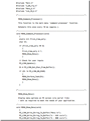
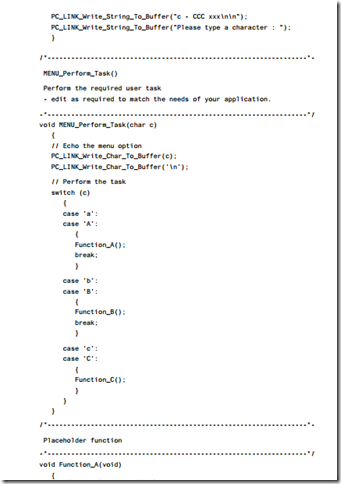
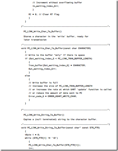
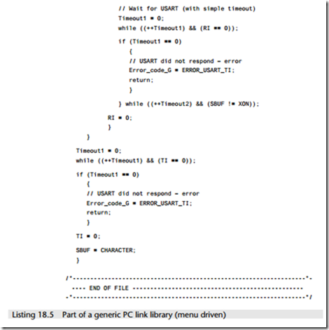
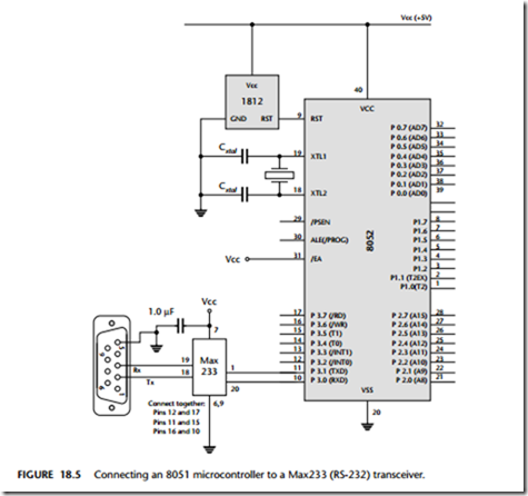
This example illustrates how to link a Standard 8051 device to a PC (listings 18.1 to 18.5). The software is menu driven in this example: the user is (via a terminal emula- tor on the PC) given the option of running one of three different tasks on the microcontroller (see Figure 18.5).

In this library, the scheduler is driven by Timer 2, and Timer 1 is used for baud rate generation.

As usual, all files for this example are included on the CD, in the directory associ- ated with this chapter.
image

image

image

image

image

image

image

image

image

image

image

image

image


Hybrid schedulers

Introduction

As we discussed in Chapter 13, co-operative schedulers provide a predictable platform for a wide range of embedded applications.

On some occasions, it can be necessary to incorporate some of the features of preemptive schedulers into a co-operative scheduler framework, in a carefully controlled manner. A hybrid scheduler seeks to achieve this.


Delays:Hardware delay

Hardware delay
Context

● You are developing an embedded application using one or more members of the 8051 family of microcontrollers.

● You are designing an appropriate software foundation for your application.

Problem

You need to wait for a fixed period of time (measured in milliseconds) before taking some action.

Background

Solution

All members of the 8051 family have at least two 16-bit timer / counters, known as Timer 0 and Timer 1. These timers can be used to generate accurate delays.

We begin by providing brief information on these timers.

Timer 0 and Timer 1

Timer 0 and Timer 1 have much in common and we will consider them together.

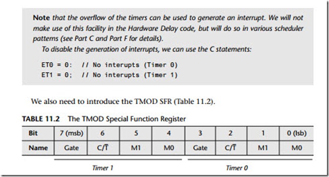
To see how these timers operate, we need, first, to introduce the TCON SFR (Table 11.1).

Delays-0189

(Cleared by hardware if processor vectors to interrupt routine.)

TR1 Timer 1 run control bit

Set/ cleared by software to turn Timer 1 either ‘ON’ or ‘OFF’.

TF0 Timer 0 overflow flag

Set by hardware on Timer 0 overflow.

(Cleared by hardware if processor vectors to interrupt routine.)

TR0 Timer 0 run control bit

Set / cleared by software to turn Timer 0 either ‘ON’ or ‘OFF’.

Note that the overflow of the timers can be used to generate an interrupt. We will not make use of this facility in the Hardware Delay code, but will do so in various scheduler patterns (see Part C and Part F for details).

To disable the generation of interrupts, we can use the C statements:

Delays-0190

The first thing to note in TMOD is that there are three main modes of operation (for each timer), set using the M1 and M0 bits. We will only be concerned in this book with Mode 1 and Mode 2, which operate in the same way for both Timer 0 and Timer 1, as follows:

Mode 1 (M1 = 0; M0 = 1)

16-bit timer/counter (with manual reload).1

Mode 2 (M1 = 1; M0 = 0)

8-bit timer/counter (with 8-bit auto-reload).1

The remaining bits in TMOD have the following purpose:

GATE Gating control

When set, timer/counter ‘x’ is enabled only while ‘INT x’ pin is high and ‘TRx’ con- trol bit is set. When cleared timer ‘x’ is enabled whenever ‘TRx’ control bit is set.

C/T

Counter or timer select bit

Set for counter operation (inputfrom ‘Tx’ input pin).

Cleared for timer operation (input from internal system clock).

Finally, before we can see how this hardware can be used to create delays, you need to be aware that there are an additional two registers associated with each timer: these are known as TL0 and TH0, and TL1 and TH1. These ‘L’ and ‘H’ refer to ‘low’ and ‘high’ bytes, as will become clear shortly.

Creating delays with Timer 0 and Timer 1

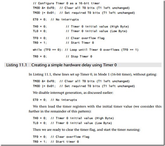
To see how this all fits together, we will consider a concrete example (Listing 11.1).

Delays-0191

What happens now in the original 8051 (we consider some exceptions under ‘Portability’) is that the timer will be incremented every 12 oscillator cycles. When this (16-bit) timer overflows – that is, it is incremented from a value of 65535 – the timer flag (TF1) will be set. In addition, as we have already noted, this overflow can be used to generate an interrupt; we do not use this option here.

This is very useful behaviour. Simply by varying the initial value stored in the timer, we specify the number of oscillations that occur before an overflow takes place and can generate shorter delays.

Building on the material discussed under ‘Background’, HARDW ARE DELA Y calcula- tions generally take the following form:

● We calculate the required starting value for the timer.

● We load this value into Timer 0 or Timer 1.

● We start the timer.

● The timer will be incremented, without software intervention, at a rate determined by the oscillator frequency; we wait for the timer to reach its maximum value and ‘roll over’.

● The rolling over of the timer signals the end of the delay by changing the value of a flag variable.

● With a 12-oscillator per instruction 8051, running at 12 MHz, the longest delay that can be produced with a 16-bit timer is ~65 ms. If we need longer delays, we can repeat the process.

Overall, this is a powerful and reliable technique and can be used to generate repeatable delays with good levels of accuracy. A detailed code example is presented later in this pattern.

Why not use Timer 2?

In many cases, as we saw in Chapter 3, modern 8051 family devices are based on the slightly later 8052 architecture: such devices include an extra, more powerful timer (called, logically, Timer 2).

While Timer 2 can be used to generate delays (in a manner nearly identical to that used with Timer 0 and Timer 1 in this pattern), this is generally an inappropriate use for this resource. This is because Timer 2 is a 16-bit auto-reload timer. This auto-reload feature has no value in the generation of delays, but makes it ideally suited as a source of ‘ticks’ for the schedulers we use throughout most of this book.2

Hardware resource implications

H ARDW ARE D ELA Y requires non-exclusive use of a timer. There are often competing demands for such resources, since they are essential for driving a scheduler and are often used, for example, to generate timeouts (see HARDW ARE TIMEOUT [page 305]), for pulse-width modulation (see 3LEVEL PWM [page 822]), for pulse-rate modulation

(see HARDW ARE PRM [page 742]) and for pulse counting (see HARDW ARE PULSE – COUNT

Reliability and safety implications

The techniques discussed in HARDW ARE DELA Y are generally more portable and more accurate than software-based delays, but they are still not suitable for generating pre- cisely timed delays without careful hand-tuning to take into account factors such as the time taken to call the delay function and the time taken to load the timer with the initial count value.

Delays generated through multiple calls to a delay function will increase the impact of these factors; long delays generated using this technique are likely to be particularly inaccurate.

Portability

We consider two main portability issues here.

Differences in timer increment rates

In the original 8051 (and in most current 8051s), Timer 0 and Timer 1 are incre- mented every 12 oscillator cycles: that is, at 1 MHz in a device using a 12 MHz crystal oscillator. In more recent 8051 devices, factors of 6, 4 or 1 are also used. You must check the data sheet to ensure that your calculations of the initial reload values take these differences into account.

Note that the library code (listed later) is itself highly portable, because it makes use of information provided in the PROJECT HEADER [page 169] file.

Porting within the 8051 family

There are limited timers available in the 8051 family. Careful use of particular timers can help make your code easier to port.

For example, in many applications presented in this book, we will use Timer 2 (where available) to drive a scheduler (see, for example, Chapter 13). In addition, in some appli- cations, Timer 1 will be required to generate baud rates, for a serial network. As a result, your delay code will be particularly portable if you base it on Timer 0.

Note that, where you will use a scheduler and a serial link and your chosen micro- controller does not have Timer 2 available, you may need to use both the available timers for the scheduler (T0) and baud rate generation (T1). You will then be forced to use an implementation of SOFTW ARE DELA Y [page 179] for any necessary delay gener- ation. Note also that, in many cases, the use of a scheduler can remove the need for most delay calculations.

Finally, note that, in addition to Timer 2, some extended 8051s have an additional internal timer, intended for use as an internal baud rate generator: this can free Timer 1 for other purposes, such as delay generation. (See Chapter 3 for details.)

Porting beyond the 8051 family

Like the 8051 family, most microcontrollers have on-board timers: where such timers are available, this pattern may be adapted without great difficulty. If your chosen microcontroller does not have an on-board timer, the pattern SOFTW ARE DELA Y [page 206] offers an alternative solution.

Overall strengths and weaknesses

These basic time delay techniques have the great advantage that they are very simple and can be implemented in a few lines of code. As a result, they are widely applicable and are frequently used in applications where very accurate timing is not of great concern.

clip_image010They are not suitable for generating very short delays; see ‘Related patterns and alternative solutions’ for alternative suggestions.

Because of the need to manually reload the initial timer value, the delays obtained may not be precisely as expected. This is of particular concern where, for example, an attempt is made to delay for (say) a second by invoking a 50 ms delay 20 times: this will not be accurate. Do not attempt to use HARDW ARE DELA Y to implement a real-time clock!

They require access to an important hardware resource (a timer).

The timings are not very portable: even different members of the 8051 family have different relationships between crystal frequency and instruction cycle fre- quency (note, however, that the code that follows addresses this problem for a wide range of delays).

As implemented here, the processor is tied up waiting for the timer to overflow. Where processor power is limited, this may not be an acceptable solution: use of a scheduler (see Chapter 13) can often reduce the need to waste CPU time in this way.

Related patterns and alternative solutions

The code we present in this pattern is designed to generate delays on N millisecond duration, which is a key requirement in many applications. If this is not what you require, then some alternatives are as follows:

● To generate delays from ~10 µs to about ~10+ ms, HARDW ARE TIMEOUT [page 305] can be used very effectively.

● For generating delays less than ~10 µs, neither HARDW ARE DELA Y nor HARDW ARE T IMEOUT – both of which use Timer 0 / Timer 1 – is suitable. For example, in an original 12 MHz 8051, the minimum timer increment is, in theory, 1 µs: that is the oscillator frequency / 12. However, this delay will often be less than the time taken to call the delay function, set up and start the timer. In general, delays less than

around 10 µs are better implemented in software: see SOFTW ARE DELA Y [page 206] (and LOOP TIMEOUT [page 298]).

● Delays waste CPU time and it is better to avoid using them at all, if possible: see CO OPERA TIVE SCHEDULER [page 255] for a delay-free alternative that will work in many circumstances.

Example: Generic delay code

Flashing an LED can be useful as a means of drawing attention to a particular warning message or error condition. It can also be used as a means of saving power. There are, of course, numerous different ways of implementing such behaviour: here, we illus- trate the use of the HARDW ARE DELA Y pattern.

Hardware

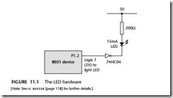
The single LED (or a similar device, such as a buzzer) is assumed to be connected to an 8051 microcontroller on Port 1 (P1.2), using positive logic: that is, +5V lights the LED (Figure 11.1).

Delays-0192

Software

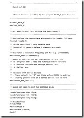
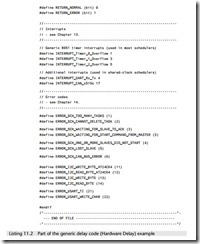
Here we use some generic delay code. This allows the initial timer values to be ‘auto- matically’ determined for a wide range of different hardware and oscillator combinations, by means of the project header file (Main.H), and some appropriate use of the C pre-processor directives.

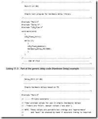
The key files required in the project follow (Listings 11.2 to 11.4). As usual com- plete set of files are included on the CD.

Delays-0193Delays-0194Delays-0195Delays-0196

Delays-0197