PIC Program Development:Program Design

Program Design

There are international standards for specifying engineering designs, which should be applied in commercial work. The design standards for different types of products will vary; for instance, a military application will typically be designed to a higher standard of reliability and more rigorously tested and documented than a commercial one. Our designs here are somewhat artificial in that they are intended to illustrate features of the PIC microcontroller, rather than meet a genuine user requirement. Nevertheless, we can follow the design process through the main steps.

Application Specification

The first step in the design process is to specify the functions and performance required by the application. In the real world, this needs to be done in some detail so that the overall design, development and production costings and timescales can be predicted as far as possible, as well

as establishing the market or customer requirements. For our purposes, the minimal specification given in Chapter 3 will suffice:

The circuit should output a binary count to eight LEDs, under the control of two push-button inputs. One input will start the output sequence when pressed. The sequence will stop when the button is released, retaining the current value on the display. The other input will clear the output (all LEDs off), allowing the count to resume from zero.

The next step is to design the hardware in which the application program will run, unless it already exists. A block diagram, which shows the user interface requirements, is a good starting point. The interfacing of the microcontroller is often implemented using certain standard devices, such as push buttons, keypad, LED indicators, LCD, relays and so on. The circuit design techniques required will not be covered in any detail here; the most common interfacing techniques and devices are described in Interfacing PIC Microcontrollers: Embedded Design by Interactive Simulation by the author (Newnes 2006). The microcontroller must be selected by specifying the requirements such as:

• Number and type of inputs and outputs (based on chip pin-out)

• Program memory size (maximum number of instructions)

• Data memory size (number of spare file registers)

• Program execution speed (clock speed)

• Availability of special interfaces (e.g. analogue inputs, serial ports).

The hardware configuration for the BINx applications has already been described in Chapter 3 (Figure 3.3). We have established that the instruction set and programming features of the microcontroller selected are suitable. If further features were required, the existing hardware design could be modified. If the microcontroller selected was then found to be lacking in some respect, for example, not enough input/output (I/O) pins, another microcontroller, or other types of hardware such as a conventional microprocessor system, may be considered. However, it is easier to stay within one family of processors, since it is normally based on a shared architecture and instruction set, from which the most suitable can be selected. The PIC range is the most extensive available for small and mid-range applications.

Microcontrollers are normally used in so-called real-time applications, typically a control system where inputs are measured and outputs modified as rapidly as possible, such as a motor vehicle engine controller. Complex data processing may be needed, but data storage is minimal. For simpler applications, assembly language provides maximum speed and minimum memory requirements, but for more complex software, a higher level language may be needed. This will provide a greater range of more user-friendly statements and constructs, such as mathematical functions and display drivers. The more powerful PIC microcontrollers are therefore generally programmed in the language C, the next level up from assembler. The basic syntax is more like English than assembler, and is therefore easier to learn and does not depend on an intimate knowledge of the MCU architecture. The downside is that each C statement

PIC Microcontrollers-1156

translates into several assembler instructions, so the program is longer and therefore slower to execute. It also needs more program memory. Programming PIC microcontrollers in C is introduced in Programming 8-bit PIC Microcontrollers in C with Interactive Hardware Simulation by the author (Newnes 2008).

Program Algorithm

A flowchart can be useful for illustrating the overall algorithm (process) graphically, particularly when learning programming. A flowchart for BIN3 is shown in Figure 4.2.

The program title is placed in the start symbol at the top of the flowchart, and the processes required are defined as a sequence of blocks. Each flowchart box will contain a description of the action at each stage, using different shaped boxes for processes (rectangle), input and output (sloping) and decisions (pointed). The decision box has two outputs, to represent a conditional branch in the program. This decision box should contain a question with the answer yes or no, and the active selection labeled YES or NO as appropriate; only output one needs to be labeled. The jump destinations can also be labeled, and these same labels can be used in the program as address labels.

Programming packages exist that allow a flowchart to be converted directly into code, which are most useful in education and training environments. Software design techniques, including flowcharts, will be discussed in more detail later.


PIC Program Development:Program Development

Program Development

The primary development system toolset for PIC applications is Microchip MPLAB IDE (integrated development environment). At the time of writing, MPLAB version 8.60 is the most recently released version. The basic principles of use do not change greatly as it is updated, rather extra facilities and support for an ever-expanding range of devices are added, and the reader will need to refer to the manufacturer’s documentation for details concerning the use of any particular version. The intention at this stage is to outline how to assemble and test demonstration programs BIN3 and BIN4. More advice on debugging programs is provided in Chapter 9.

The flowchart in Figure 4.1 gives an overview of the program development process.

The starting point is the specification for the program, which describes how the application will function when complete. This must then be analyzed by the software designer so that the required program can be derived from it, taking into account the features of the instruction set of the microcontroller (MCU). The program algorithm describes the process whereby the required outputs are obtained from the given inputs. Various software design techniques are available to outline the program, including flowcharts and pseudocode, which we will use here. These represent the program processes and their sequence in

PIC Microcontrollers-1154

The source code is developed from the program algorithm by filling in the details and converting each program block to assembler code. The program must be saved regularly as it is developed; it is a good idea to always have backup copies on different disks (memory stick, hard disk or network drive) in case of disk, memory or network failure. The source code text file is called PROGNAME.ASM, where PROGNAME represents the application name, such as BIN1. Successive versions of a program can be numbered BIN1, BIN2, etc., so that we can revert to an earlier version if new code does not work properly.

After initial text entry, the program can be assembled by calling up the assembler utility, MPASMWIN.EXE. It converts the source code into machine code, and creates additional files to help with debugging (fault finding) the program. If a mistake has been made in the individual instruction (e.g. misspelling a mnemonic), it will be reported in an error message window and an entry added to the error file on disk. This must then be corrected in the source code and the program reassembled until it is free of syntax errors.

The program can then be tested for correct operation by simulation, using the Microchip MPLAB simulator MPSIM or Proteus VSM (ISIS). This means running the program in the host computer as though it were running in the chip itself. The program is loaded and executed on screen, and the outputs are observed. It can then be checked step by step for the correct logical operation, by monitoring the changes in the registers, and checking the timing if necessary. Simulated inputs are needed to represent all the likely input sequences and combinations. If a logical error is found, the source code must be re-edited and reassembled, and the simulation repeated.

This process is simpler in ISIS, since inputs can be generated interactively on the schematic (see Figure 3.3) from animated manual inputs or simulated signals. Outputs can be observed directly on light-emitting diodes (LEDs), seven-segment displays or liquid crystal displays (LCDs), or on virtual instruments such as oscilloscopes or logic analyzers. However, MPLAB has the advantage that inputs and outputs can be generated from a predefined stimulus file and outputs recorded in a trace file, which provides a form of automated testing using standard sequences and a permanent record of the test results. Thus, MPSIM has a more extensive range of debugging tools, but Proteus can test the whole circuit and is more intuitive.

When the logical errors have been removed, the program can be downloaded to the chip. Final testing can then allow the finished circuit function to be compared with the original specification. If necessary, in-circuit debugging can be used to detect any remaining errors that may arise from interaction with the real peripheral circuits. Most current PIC chips have

on-board circuitry to support this option, while smaller chips need a dedicated header connector (see Chapter 7). Only MPSIM provides this final debugging stage.

The main software tools and the files created and used by MPLAB during the development process are listed in Table 4.1. The most significant ones are the source code (.ASM) and

PIC Microcontrollers-1155

machine code (.HEX) for simulation and downloading. The error file (.ERR) stores the assembler error messages that are displayed automatically when generated. The list file (.LST) contains the source text, machine code, memory allocation and label values in one text file. In more complex applications, multiple relocatable machine code object files (.O) that have been assembled separately as application components are combined by a linker utility to produce a COF file which contains the hex and list files (see Microchip ‘MPASM User’s Guide’).


A Simple PIC Application:Assembly Language

Assembly Language

It should be apparent that writing the machine code manually for any but the most trivial applications is going to be a bit tedious. Not only do the actual hex instruction codes have to be worked out, but so do jump destination addresses and so on. In addition, the codes are not easy to recognize or remember.

Mnemonics

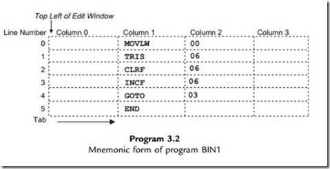
For this reason, simple microcontroller programs are written in assembly language, not machine code. Each instruction has a corresponding mnemonic defined in the instruction set. The main task of the assembler program supplied with the chip is to convert a source code program written in mnemonic form into the equivalent machine code. The mnemonic form of the program BIN1 is shown in Program 3.2.

PIC Microcontrollers-1149

The instructions can now written as recognizable (when you get used to them!) code words. The program is typed into a text editor, spaced out as shown, using the tab key to place the code in the correct columns. Note that the first column (column 0) is kept blank; we will see why later. The instruction mnemonics are placed in column 1, and the operands (data to be operated on) in column 2. The operand 00 is the data direction code for the port initialization, 06 is the file register number of the port data register, and 03 is the jump destination address, line 3 of the program. The PIC instructions are all 14 bits long, so each line of source code becomes a 14-bit code, which we have already seen. The meaning of the mnemonics is as follows:

PIC Microcontrollers-1150

The END statement is an assembler directive; it tells the assembler that this is the end of the program, and is not converted into an actual instruction. When entering the program, there must be space before and after each instruction mnemonic, and it is advisable to lay out the program in columns as shown to improve its readability.

Assembly

The source code program could be created using a general purpose text editor, but is normally edited within a dedicated software package such as MPLAB, the PIC integrated development environment (IDE), which contains the assembler as well as a text editor. ISIS schematic capture also incorporates a suitable text editor, which can be opened after the circuit drawing has been completed, or it can be run in conjunction with MPLAB.

The source code text is entered in an edit window and the assembler invoked from the menu. The assembler program analyzes the source code, character by character, and works out the binary code required for each instruction. The terminology can be confusing here; the assembly language application program (user source code) is created in the text editor, while the software tool that performs the conversion is the assembler program or utility.

The source code is saved on disk as a text file called PROGNAME.ASM, where ‘progname’ represents any suitable filename. This is then converted by the assembler program MPASM.EXE, which creates the machine code file PROGNAME.HEX. This appears as hexadecimal code when listed. At the same time, PROGNAME.LST, the list file, is created, containing both the source and hex code, which may be useful later on when debugging (fault finding) the program, we have already seen KEY690.LST in Chapter 1. This assembly and download process will be described in more detail in the next chapter.

Labels

The mnemonic form of the program with numerical operands can now be further improved. We want the operands to be specified in a more easily recognizable form, in the same way that the mnemonics represent the instruction codes. Therefore, the assembler is designed to recognize labels.

A label is a word that represents a number, which can be an address, register or literal. Examples used below are ‘again’, ‘portb’ and ‘allout’. These are listed at the top of the program with the replacement value, and the assembler simply replaces any occurrence of the label with the corresponding number.

Jump destinations are similarly defined by label, by placing the label at the beginning of the destination line, and using a matching label as the jump instruction operand. When the program is assembled, the assembler notes the numerical address of the instruction where the label was found, and replaces the label, when found as an operand, with this address.

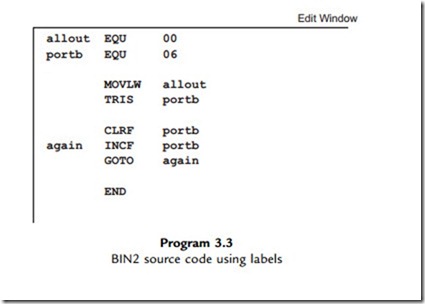
The program BIN1 can thus be rewritten using labels as shown in BIN2 source code (Program 3.3). The literal value 00 and the port register address 06 have been replaced with labels, which are assigned at the beginning of the program. The ‘equate’ statements define the numbers that are to be replaced in the source code. In this case, the label ‘allout’ will represent the port B data direction code, while the data register address itself, 06, will be

PIC Microcontrollers-1151

represented by the label ‘portb’. ‘EQU’ is another example of an assembler directive, which is an instruction to the assembler program and will not be translated into code in the executable program.

Note that lower case is used for the labels, while upper case is used for the instruction mnemonics and assembler directives. Although this is not obligatory, this convention will be used because the instruction mnemonics are given in upper case in the instruction set. The labels can then be distinguished by using lower case. The jump destination label is simply defined by placing it in column 0 of the line containing the destination instruction. The ‘GOTO label’ instruction then uses a matching label. Initially, labels will be limited to six characters; they must start with a letter, but can contain numbers, e.g. ‘loop1’. Longer labels may be used if preferred.

The programs BIN1 and BIN2 are functionally identical, and the machine code will be the same.

Layout and Comments

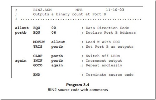
A final version of BIN2 (Program 3.4) includes comments in the program to explain the action of each line, and the overall program. As much information as possible should be provided. When learning programming, comments help the learner to retain information, and when developing real applications, it will help with future modifications and upgrading or software maintenance. Even if you have written the program yourself, you may have forgotten how it works later on!

Comments must be preceded by a semicolon (;), which tells the assembler to ignore the rest of that line. Comments and information can thus occupy a whole line, or can be added after

PIC Microcontrollers-1152

PIC Microcontrollers-1153

each instruction in column 3. A minimal header has been added to BIN2, with the source code file name, author and date, and a comment added to each line. Blank lines can be used without a comment ‘delimiter’ (the semicolon); these are used to break up the source code into functional sections, and thus make the structure of the program easier to understand. In BIN2.ASM, the first block contains the operand label equates, the second the port initialization and the third the output sequence. The layout of the source code is very important in showing how it works.

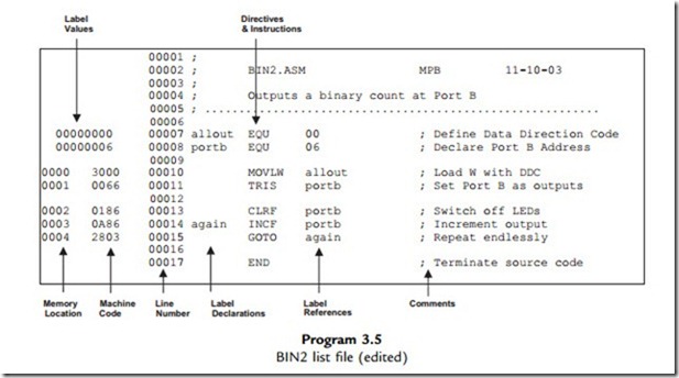
The list file for the program BIN2 is provided as Program 3.5. It contains the source code, machine code and program memory addresses in one file. It has been edited to remove extraneous detail; the original may be downloaded from www.picmicros.org.uk with all the other demo application filesets. A complete list file may be seen in Table 4.4 (Chapter 4).

We now have a program that can be entered into a text editor, assembled and downloaded to the PIC chip. The exact method will vary with the development system you are using. Next, we will look in more detail at developing the program.

. State the four-digit hex code for the instruction INCF 06. (2)

2. State the two-digit hex code for the instruction MOVLW. (2)

3. What is the meaning of the least significant two digits in the PIC machine code

instruction 2803? (2)

4. Why must the instruction mnemonic be in the second column of the source code? (2)

5. Give two examples of a PIC assembler directive. Why are they not represented in the machine code? (3)

6. What are the numerical values of the labels ‘allout’ and ‘again’ in BIN2? (2)

7. A line from the list file for BIN2 is shown below. Explain the significance of each item. (6)

0003 0A86 00014 again INCF portb

8. State the function and origin of program files with the extension: (a) ASM, (b) HEX,

(c) LST. (6)

Answers on page 419. (Total 25 marks)

Activities 3

1. Check the machine code for BIN1 against the information given in the PIC instruction set in the data sheet, so that you could, if necessary, write a program entirely in machine code. Modify the machine code program by deleting the ‘Clear Port B’ operation and changing the ‘Increment Port B’ to ‘Decrement Port B’. What would be the effect at the output when the program was run? Suggest an alternative to the instruction MOVLW 00 which would have the same effect.

2. Refer to Appendix E for a guide to using Proteus VSM to simulate the circuit. You will need a version of Proteus that includes the working model of the 16F84A chip. Enter or download the schematic BIN.DSN into ISIS and attach the program BIN1.ASM. Check that it assembles and runs correctly. Display the SFRs and source code. Set the MCU simulated clock to 100 kHz and single step the program. Observe the execution sequence, and check that the time taken to complete one loop is 120 ms.

3. Enter the program BIN2, using labels, into the text editor, assemble and test as above. Display or print out the list file BIN2.LST and check that the machine code generated is the same as BIN1. Note that there is no machine code generated for comment lines or assembler directives.

If necessary, refer forward to relevant sections to complete these activities.


A Simple PIC Application:Program BIN1 and Program Analysis

Program BIN1

The simple program called BIN1 is shown as Program 3.1. It consists of a list of 14-bit binary machine code instructions, represented as four-digit hex numbers (see Chapter 2). Bits 14 and 15 are assumed to be zero, so the codes are represented by hex numbers in the range 0000 to 3FFF. The program is stored at hex addresses 0000 to 0004 (five instructions) in program memory.

Program Analysis

The program instructions must be related to the PIC internal architecture, as outlined in Chapter 2, and specified in the data sheet. The instruction set in the data sheet explains the significance of each bit in each instruction.

PIC Microcontrollers-1147

This is a jump instruction, which causes the program to go back and repeat the previous instruction. This is achieved by the instruction overwriting the current program counter contents with the value 03, the destination address, which is given as the last two digits of the instruction code. The execution point is thus forced back to the previous instruction, so the program keeps repeating indefinitely. Most control programs have the same basic structure as this simple example; an initialization sequence and an endless loop, which will read the inputs and modify the outputs.

Program Execution

BIN1 is a complete working program, which initializes and clears port B, and then keeps incrementing it. The last two instructions, increment port B and jump back, will repeat indefinitely, with the value being increased by one each time. In other words, port B data register will act as an 8-bit binary counter. When it reaches FF, it will roll over to 00 on the next increment operation.

If you study the binary count table seen in Appendix A (Table A.3), you can see that the least significant bit is inverted each time the binary count is incremented. The least significant bit (LSB), RB0, will thus be toggled (inverted) every time the increment operation is repeated. The next bit, RB1, will toggle at half this rate, and so on, with each bit toggling at half the frequency of the previous bit. The most significant bit (MSB) therefore toggles at 1/128 of the frequency of the LSB. The output pattern generated is shown in Figure 3.5.

A PIC instruction takes four clock cycles to complete, unless it causes a jump, in which case it will take eight clock cycles (or two instruction cycles). The repeated loop in BIN1 will therefore take 4 þ 8 ¼ 12 clock cycles, and it will take 24 cycles for the RB0 to go low and high, the output period of the LSB. If the CR clock is set to run at 100 kHz, the clock period is 1/105 s ¼ 10 ms (frequency ¼ 1/period), giving an instruction cycle time of 40 ms. The loop will take 12 x 10 ¼ 120 ms, giving an output period of 240 ms, a frequency of 4167 Hz, and RB7 will then flash at 4167/128 ¼ 32.5 Hz. These outputs can be displayed on an oscilloscope or logic analyzer (virtual or real).

PIC Microcontrollers-1148

In the real hardware, the output changes too quickly to see unaided, but it is possible to reduce the clock speed by increasing the value of the resistance and/or the capacitor in the clock circuit. We will see later how to slow the outputs down without changing the clock, by adding a delay routine. In simulation mode, as we will see later, the timing can also be checked using debugging tools such as the stopwatch in MPLAB or the timing display in Proteus VSM.

The frequencies generated are actually in the audio range, and they can be heard by passing them to a small loudspeaker or piezo buzzer. This is a handy way of checking quickly that the program is working, and also immediately suggests a range of PIC applications e generating signals and tones at known frequencies. We will come back to this idea later, and see how to generate audio outputs, or a tone sequence to make a tune, such as a mobile phone ring tone.


A Simple PIC Application:Program Execution

Program Execution

Microcontroller circuits will not function without a program in the chip; this is created using the PIC development system software on a PC, and downloaded via a serial data link. This process has already been outlined, and will be described in more detail later, so for now we will assume that the program is already in memory.

Figure 3.4 is a block diagram showing a simplified program execution model for the PIC 16F84A. The main elements are the program memory, decoder, working register and file registers. The binary program, in hexadecimal, is stored in the program memory. The instructions are decoded one at a time by the instruction decoder, and the required operations set up in the registers by the control logic. The file registers are numbered from 00 to 4F, with the first 12 registers (00 to 0B) being reserved for specific purposes. These are called the special function registers (SFRs). The rest may be used for temporary data storage; these are called the general purpose registers (GPRs). Only selected registers are shown in this diagram. All addresses and register contents are in hexadecimal. Appendix A explains hexadecimal numbers.

PIC Microcontrollers-1146

3.2.1. Program Memory

The program memory is a block of flash read-only memory (ROM), which means it is non- volatile, but can be reprogrammed. The program created in the host computer is downloaded via port register pins RB6 and RB7. The methods for doing this will be described in more detail in Chapter 4, as will the assembler programming language required to create the program code.

The 14-bit codes are loaded into memory starting at address 000. When the chip is powered up, the program counter resets automatically to 000, and the first instruction is fetched from this address, copied to the instruction register in the control block, decoded and executed. The file registers are modified accordingly, and the resulting output seen at the ports.

3.2.2. Program Counter, PCL: File Register 02

The program counter keeps track of the program execution by holding the address of the current instruction. It is automatically incremented to point to the next instruction during the execution cycle. If there is a jump in the program, the program counter is modified by the jump instruction (e.g. the last one in this program), so that it then points to the required jump destination address. PCLATH stands for program counter latch high. This stores the most significant two bits of the 10-bit program counter, which also cannot be accessed directly.

3.2.3. Working Register, W

This is the main data register (8 bits), used for holding the data that is currently being worked on. It is separate from the file register set and is therefore referred to as W in the PIC program. Literals (values given in the program) must be loaded into W before being moved to another register or used in a calculation. Most data movements have to be via W, in two stages, since direct moves between file registers are not available in the basic PIC instruction set.

3.2.4. Port B Data Register, PORTB: File Register 06

The 8 bits stored in the port B data register will appear on the LEDs connected to pins RB0eRB7, if the port bits are initialized as outputs. The data direction for each pin is determined by placing a data direction code in the register TRISB. A ‘0’ in TRISB sets the corresponding pin in the port register as an output (0 ¼ output). A ‘1’ sets it to input

(1 ¼ input). In this case, 00000000 (binary) will be placed in TRISB to set all bits as outputs, but any combination of inputs and outputs can be used.

3.2.5. Port A Data Register, PORTA: File Register 05

The least significant five bits of File Register 05 are connected to pins RA0eRA4, the other three being unused. Inputs RA0 and RA1 will be used later to read the push buttons. If not initialized as outputs, the PIC I/O pins automatically become inputs, i.e. TRISA ¼ xxx11111. We will use this default setting for port A, so this port does not have to be explicitly initialized. The state of these inputs will have no effect unless the program actually uses them; the first program BIN1 will not use them.

3.2.6. General Purpose Register 1, GPR1: File Register 0C

The first GPR will be used later in a timing loop. It is the first of a block of 68 such registers, numbered 0C to 4F in the ’84A chip. They may be allocated by the programmer as required for temporary data storage, counting and so on.

3.2.7. Bank 1 Registers

The main registers such as the program counter and port data registers are in a random access memory (RAM) block called register bank 0, while TRISA, TRISB and PCLATH are in a separate block, bank 1. Bank 0 can be directly addressed, meaning that data can be moved into it using a simple ‘move’ instruction.

Unfortunately, this is not the case with bank 1. There are two ways to write to these registers. The first way is a simple method, which we will use initially; it requires the required 8-bit code to be loaded into W first, and then moved into the bank 1 register using the TRIS instruction. Later, we will use the recommended method, using bank selection, but this is a little more complicated. TRIS does not now appear in the main instruction set, but continues to be recognized by the PIC assembler.


A Simple PIC Application:BIN Circuit Operation

BIN Circuit Operation

Active low switch circuits, consisting of normally open push buttons and pull-up resistors, are connected to the control inputs; the resistors ensure that the inputs are high when the buttons

PIC Microcontrollers-1145

are not pressed. The outputs are connected to LEDs in series with current-limiting resistors. The PIC outputs are capable of supplying enough current (up to 20 mA) to drive LEDs directly, making the circuit relatively simple. The external clock circuit consists of a capacitor (C) and resistor (R) in series; the value of C and R multiplied together will determine the chip clock rate. The resistance in this circuit has been made variable, and the values shown should allow the clock frequency to be adjusted to 100 kHz. The reset input (!MCLR) must be connected to the positive supply (þ5 V). Other unused pins can be left open circuit, and unused input/output (I/O) pins will default to inputs.


A Simple PIC Application:BIN Hardware Block Diagram

BIN Hardware Block Diagram

The hardware arrangement can be represented in simplified form as a block diagram (Figure 3.2). This is not really necessary for such a trivial circuit, but is a useful system design technique for more complex applications. The main parts of the hardware and relevant inputs

PIC Microcontrollers-1143

PIC Microcontrollers-1144

and outputs should be identified, together with the direction of signal flow. The type of signal can be indicated, e.g. parallel or serial data, or analogue waveform. The power connections need not be shown; it is assumed that suitable supplies are available for the active components. The idea is to outline the basic hardware arrangement without having to design the circuit in detail at this stage.

Port A (5 bits) and port B (8 bits) give access to the data registers of the ports, the pins being labelled RA0 to RA4, and RB0 to RB7, respectively. The two push-button switches will be connected to RA0 and RA1, and a set of LEDs connected to RB0 to RB7. The switches will later be used to control the output sequence. However, these inputs will not be used in the first program, BIN1. The connections required are shown in Table 3.2.

The block diagram can now be converted into a circuit diagram. A drawing is created using electronic schematic capture software such as Proteus VSM (ISIS) or ORCAD. In Proteus, the design file can then be used to test the circuit by interactive simulation. When finalized, it can be converted into a printed circuit board and the hardware produced. The schematic can be inserted into other documentation as required, or printed separately.

The schematic for the BIN circuit design created in ISIS (BIN.DSN) is shown in Figure 3.3. This is available on the support website www.picmicros.org.uk and can be used to simulate the circuit operation described below. The process for editing the schematic and simulating the circuit operation is described in Appendix E. The operation of the chip itself can be simulated in MPLAB, the Microchip development system.


A Simple PIC Application:Hardware Design and PIC 16F84A Pin-Out

Hardware Design

We need a microcontroller that will provide two inputs and eight outputs, which will drive the light-emitting diodes (LEDs) without additional interfacing, and has reprogrammable flash memory to allow the program to be developed in stages. An accurate clock is not required, so a crystal oscillator is not necessary. The PIC 16F84A meets these requirements; it is a basic device, so we will not be distracted by unused features. Later, we can replace it with a more recent processor, such as the PIC 16F690. The 16F84A should not be used for new designs.

PIC 16F84A Pin-Out

The PIC 16F84A microcontroller is supplied in an 18-pin dual in-line (DIL) chip. The pin labeling, taken from the data sheet (download from www.microchip.com), is shown in Figure 3.1. Some of the pins have dual functions, which will be discussed later.

PIC Microcontrollers-1142

The chip has two ports, A and B, consisting of five and eight pins, respectively. The port pins allow data to be input and output as digital signals, at the same voltage levels as the supply, which is connected between VDD and VSS, nominally 5 V. CLKIN and CLKOUT are used to connect clock circuit components, and the chip then generates a fixed frequency clock signal that drives all its operations along. !MCLR (NOT Master CLeaR) is a reset input, which can be used to restart the program. Note that the active low operation of this input is indicated by a bar over the pin label in the data sheet, or an exclamation mark here. In simple applications, this input does not need to be used, but it MUST be connected to the positive supply rail to allow the chip to run. If you construct a circuit and it does not work, check this point. A summary of the pin functions is provided in Table 3.1.

Port B has eight pins, so we will assign these pins to the LEDs and initialize them as outputs. Port A has five pins, two of which can be used for the input switches. A resistor and capacitor will be connected to the CLKIN pin to control the clock frequency. In this chip, an external crystal can be used for a more precise clock frequency, and in many current chips, an internal oscillator is provided, which means that no external clock components are needed.


Microcontroller Operation:Conditional Jump

Conditional Jump

The conditional jump instruction is required for making decisions in the program.

Instructions to change the program sequence depending on, for instance, the result of a calculation or a test on an input, are an essential feature of any microprocessor instruction set.

PIC Microcontrollers-1136

In Figure 2.3, the code 1885 tests an input bit of the PIC and skips the next instruction if it is zero. Instruction YYYY (representing any valid instruction code) is then executed. If the input bit is high, the instruction 2807 is executed, which causes a jump to address 007, and instruction ZZZZ is executed next. This is called Bit Test and Skip, and is the way that conditional branches are achieved in the PIC.

In PIC assembly language, this program fragment looks like this:PIC Microcontrollers-1137

The PIC is designed with a minimal number of instructions, so the conditional branch has to be made up from two simpler instructions. The first instruction tests a bit in a register and then skips (misses out) the next instruction, or not, depending on the result. This next instruction is usually a jump instruction (GOTO or CALL). Thus, program execution continues either at the instruction following the jump, if the jump is skipped, or at the jump destination.

The program outline of a conditional jump used in a delay routine, would look like this:

PIC Microcontrollers-1138

PIC Microcontrollers-1139

This software timing loop simply causes a time delay in the program, which is useful, for instance, for outputting signals at specific intervals. A register is used as a down counter by loading it with a number, XX, and decrementing it repeatedly until it is zero. A test instruction then detects that the zero flag has gone active, and the loop is terminated. Each instruction takes a known time to execute, therefore the delay can be predicted.

An example of a conditional jump can be seen at lines 39 and 40 in the keypad program, where BTFSS DIGIT,4 is followed by GOTO Next, so that the jump back is only executed if bit 4 of the register labelled DIGIT (GPR 20) is zero.

Subroutine

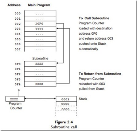
Subroutines are used to carry out discrete program functions. They allow programs to be written in manageable, self-contained blocks, which are then executed as required, often more than once per program cycle. The instruction CALL is used to jump to a subroutine, which must be terminated with the instruction RETURN.

CALL has the address of the first instruction in the subroutine as its operand. When the CALL instruction is decoded, the destination address is copied to the PC, as in the GOTO instruction. In addition, the address of the next instruction in the main program is saved in the ‘stack’, a special set of registers. The return address is ‘pushed’ onto the stack when the subroutine is called, and ‘pulled’ back into the program counter at the end of the routine, when the RETURN instruction is executed. These addresses are automatically stored in order and retrieved in reverse order.

In Figure 2.4, the subroutine is a block of code whose start address has been defined by label as 0F0. The CALL instruction at address 002 contains the destination address as its operand. When this instruction is encountered, the processor carries out the jump by copying the destination address (F0h) into the program counter. At the same time, the address of the next instruction in the main program (003) is pushed onto the stack, so that the program can come back to the original point after the subroutine has been executed.

One advantage of using subroutines is that the block of code can be used more than once in the program, but only needs to be typed in once. A delay loop can be written as a subroutine. In a program to generate an output pulse train, it can be ‘called’ twice within a loop, which sets an output high, delays, sets the output low, and delays again before repeating the whole process. The delay subroutine can be written such that it takes its delay count from W each time it is called, making it a variable delay routine, as shown in the outline below:

PIC Microcontrollers-1140

An example of a subroutine call is included in the keypad program at line 38, CALL Scan, which causes a jump to the subroutine starting at line 54. RETURN is encountered at line 83, when the execution continues from line 39.

A simple application will be developed in the next chapter to illustrate the basic principles of assembly language programming.

1. Outline the sequence of program execution in a microcontroller, describing the role of the program memory, program counter, instruction register, instruction decoder, and timing and control block. (5)

2. A register is loaded with the binary code 01101010. The carry bit is set to zero. State the contents of the register after the following operations on this data (refer to PIC MCU data sheet for exact effects):

(a) clear, (b) increment, (c) decrement, (d) complement, (e) rotate right, (f) shift left,

(g) clear bit 5, (h) set bit 0. (8)

3. A source register is loaded with the binary code 01001011, and a destination register loaded with 01100010. State the contents of the destination register after the following operations:

(a) MOVE, (b) ADD, (c) AND, (d) OR, (e) XOR. (5)

4. In a microcontroller program, a subroutine starts at address 016F and ends with a ‘return’ instruction at address 0172. A ‘call subroutine’ instruction is located at address 02F3. Assuming that the microcontroller has one complete instruction in each address, list the changes in the contents of the program counter and stack between the time of execution of the instruction before the call and the instruction following the call. Indicate an unknown value as XXXX. (5)

5. Write a program outline for the process by which two numbers, say 4 and 3, could be multiplied by successive addition. Use the register instructions Clear, Move, Add, Decre- ment, Test for Zero and Jump if Zero to Label. Load a register with zero, and add 4 to it three times by using a counter initially loaded with 3 and decremented to zero to control the loop. (7)

Answers on page 417 (Total 30 marks)

Activities 2

Download the PIC 16F84A data sheet from www.microchip.com.

1. Study the PIC 16F84A block diagram (data sheet Figure 1-1), and identify the features described in Section 2.1. Note the separate internal instruction and data buses, and summarize the function of each block. Describe how data is moved between registers and memory, and the function of the multiplexers (refer to Appendix C).

2. Study the PIC Instruction Set (data sheet Table 7-2). Note the format of the binary code for each instruction, and identify the meaning of the symbols f, b, k, d, x, C, DC and Z. Explain why some instructions take two cycles.

3. Study the list file generated for program BIN4 shown in Figure 4-4, noting the machine code at the lower left. The program memory addresses from 0000 to 000F appear in column 1, and the machine code instructions appear in column 2. Refer to the instruction set in the PIC 16F84A data sheet, and analyze the program by deducing the code for each instruction and operand, identifying SFR and GPR addresses, register bits, destination bit, address labels and literal values as appropriate. Complete the table below (for all addresses from 0004 through 000F), analyzing each instruction e 0000 to 0003 have been completed as an example:

PIC Microcontrollers-1141


Microcontroller Operation:Program Control

Program Control

As we have already seen, the microcontroller program is a list of binary codes in the program memory, which are executed in sequence. The sequence is controlled by the program counter, (PC). Most of the time, PC is simply incremented by one to proceed to the next instruction. However, if a program jump (branch) is needed, PC must be modified, that is, the address of the next instruction required loaded into PC, replacing the existing value.

The PC is cleared to zero when the chip is reset or powered up for the first time, so program execution starts at address 0000. The clock signal then drives the execution sequence forward. During the execution cycle of the first instruction, the PC is incremented to 0001, so that the processor is ready to execute the next instruction. This process is repeated unless there is a jump instruction.

The jump instructions must have a destination address as the operand. This can be given as a numerical address, but this would mean that the instructions would have to be counted up by the programmer to work out this address. So, as we can see in the program examples, a destination address is usually specified in the program source code by using a recognizable label, such as ‘again’, ‘start’ or ‘wait’. The assembler program then replaces the label with the actual address when the assembler code is converted to machine code.

Program sequence control operations are illustrated in Figures 2.2e2.4. The diagrams show the program memory from address zero, with different types of jump instruction at address 0002.

Jump

The unconditional jump (Figure 2.2) forces a jump to another point in the program every time it is executed. This is carried out by replacing the contents of the program counter with the address of the destination instruction, in this case, 005. Execution then continues from the new address. Note that the code for GOTO is 28 combined with the destination address 05, giving the instruction code 2805h.

PIC Microcontrollers-1135

The label ‘start’ is placed in the first column of the program code, to differentiate it from the instruction mnemonics, which must be placed in the second column, as we will see. The spelling of the label and its reference must match exactly, including upper and lower case letters. The label is replaced by the corresponding address by the assembler when creating the machine code for the GOTO instruction.

An example of an unconditional jump in the keypad program can be seen at line 50, GOTO Next, where Next is the label assigned to line 37.