Program Debugging:Test Schedule

Test Schedule

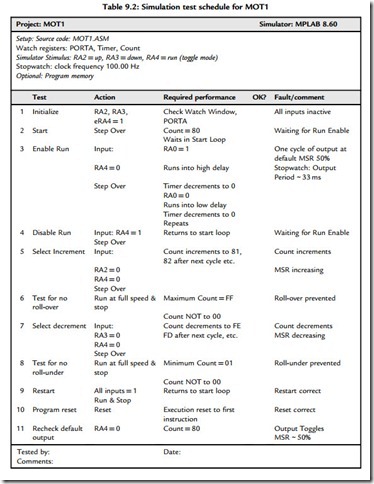
Using the simulator, the program function can be tested against the design requirements. The specification for MOT1 has been converted into a test procedure designed to exercise all its functions; we also need to anticipate incorrect input sequences that may cause a problem.

PIC Microcontrollers-1247

It is difficult to anticipate exactly what kinds of logical errors will arise, as they are generally the result of inexperience, but the following are typical:

• Port initialization: If a port does not appear to respond to output operations, check that the initialization is correct.

• Register operations: If a register is not responding as it should, ensure that the correct register is being modified, and the address label is correct. Check for correct bank selection during setup.

• Bit test & skip: Obtaining the correct sequence of operations in the program depends on these instructions. Make sure the skip condition logic is correct, as it is easy to get this wrong.

• Jump destinations: Make sure that the destination specified is correct, and the loop sequence includes all the necessary steps.

• Program structure: If the program gets lost during subroutine execution, check that call address labels are correct, and all subroutines are terminated with ‘return’ instructions.


Application Design:Hardware Design

Hardware Design

The hardware is typically designed before the software, although it may need to be revisited subsequently. It is possible that the initial choice of MCU may need to be changed when the overall design requirements have been finalized.

Block Diagram

In the block diagram, the system inputs and outputs can be identified, and a provisional arrangement of subsystems worked out. The blocks and their connections should be labeled, indicating their function. The direction and type of information flow between the blocks should be described using arrows. Inset diagrams can be used to illustrate the waveform of analogue signals. Parallel data paths will be shown as block arrows, or with suitable signal labeling. The block diagram for MOT1 is seen in Figure 8.2.

The block diagram can be readily created using the drawing tools in Microsoft® Word or a general purpose drawing package, since it needs only basic shapes, arrows and text boxes. In Word, the drawing toolbar may need to be selected via the main menu, ‘View, Toolbars, Drawing’. The drawing can be embedded in a text file, but beware of interaction of drawing objects with the text cursor, which can disrupt the drawing. It is usually a good idea to move the text cursor below the drawing area. A drawing grid can be switched on to help line up the main drawing objects; from the ‘Draw’ menu, select ‘Grid’ and check the ‘Snap to grid’ option. To make fine adjustments to drawing objects, the grid can later be switched off. It may be found that drawing directly onto the text page by switching off the default option of inserting a drawing canvas is more convenient (Tools, Options, General).

The main elements can be drawn using text boxes, and the same object used for labeling with the ‘No line’ and ‘No fill’ options selected. Various line and arrow styles are available, and the ‘Freeform’ line style in the ‘Autoshapes’ menu is useful for multi-segment lines. This menu also provides various standard shapes for block diagrams and flowcharts. When the drawing is

PIC Microcontrollers-1231

finished, select all the drawing elements by looping with the ‘Select objects’ tool and select ‘Draw, group’. This will create a single drawing object, which will no longer be affected by the text cursor, and allows the whole drawing to be repositioned on the page if necessary.

Hardware Implementation

Unless the program is being written for an existing hardware system, the general hardware configuration must be worked out as part of the design exercise. The nature and complexity of the software are important considerations in the selection of a microprocessor or microcontroller, as are the number and type of inputs and outputs, data storage and interfacing.

Various types of control system could be applied here, some of which are described in more detail in Chapter 14. The requirement is for minimal complexity with no special interfacing. A purely hardware solution could be based around the 555 timer, a standard pulse generator chip whose output is controlled by external CR (analogue) networks. However, this would not provide the push-button (digital) continuously variable output required. The microcontroller also provides a more flexible solution, in that the software is easily reconfigured.

A circuit derived from the block diagram is shown in Figure 8.3. The input control uses simple active low push buttons, with the additional feature of connections for remote system control. The motor is controlled by an FET, which acts as a current switch operated by the PIC digital output. An FET is selected whose input gate operates at TTL levels (0 Vor þ5 V with respect to the source terminal), so that it can be connected directly to the PIC output, and can handle the motor current anticipated (about 500 mA for a small motor). The motor forms an inductive

PIC Microcontrollers-1232

PIC Microcontrollers-1233

load, so a diode is connected to protect the FET from the back electromotive force (emf) normally generated by the motor. Additional decoupling is applied across the supplies to prevent the motor switching transients from disrupting the PIC supply.

The microcontroller only needs four input/output (I/O) pins, so a 12XXX series device with six I/O could be considered. However, an external reset is required, so our basic device 16F84A will be used, at least for simulation purposes. The controller I/O allocation can then be specified as shown in Table 8.2.

The PIC thus provides motor speed control with a PWM output at RA0. The !RUN (‘Not Run’, active low) input has been allocated to RA4. This will be programmed to enable the PWM output to run the motor when low. When RA2 (!UP) is low, the MSR at RB0 should increase, and the motor speed up. When RA3 (!DOWN) is low, the MSR should be reduced, slowing the motor down. !MCLR (Master Clear) is the reset input to the PIC, which will restart the program when pulsed low, and hence reset the speed to the default value of 50% MSR.


Program Debugging:Syntax Errors

Syntax Errors

When the program source code for a PIC program has been created in the editor, it must be converted into machine code for downloading to the chip. This is carried out by the

assembler program, MPASMWIN.EXE, which analyzes the source code text line by line, converts the instruction mnemonics into a list of corresponding binary codes and saves it as PROGNAME.HEX for downloading into the chip. Only valid statements as defined in the PIC instruction set will be recognized and successfully converted. Assembler directives provide additional programming instructions, but these are not converted to machine code (see Chapter 6).

Before starting a project, create a folder to keep the project files in, named, for example, MOT1. In MPLAB, the source code is created in an edit window opened by hitting the New File button. Type in the file name and save it immediately in the application folder as MOT1.ASM, or any file name with an ASM extension. It is a good idea to keep a backup version of the file set on a different drive (USB stick, portable drive or network).

When the program has been entered and saved, the project menu item ‘Quickbuild’ will assemble a single file. If required, a project can be created, but this is only really necessary for more complex applications using multiple source files or a higher level language (usually C). In the Project menu, select ‘New .’ and call the project MOT1, or the same name as the source code. Now select ‘Add Files to Project .’ and select the source code created above. The program can now be assembled by selecting ‘Build All’, and the project saved. Alternatively, the workspace can be saved, that is, the screen configuration and working files.

In the source code file, numerical formatting, assembler directives and so on must all be used correctly. If they are not, error messages will be generated when the program is assembled. These describe the syntax errors that have been found. The error messages are saved in a text file PROGNAME.ERR, and displayed when the assembler is finished. A typical set of messages is shown below:

PIC Microcontrollers-1243

To generate this list, deliberate errors were introduced into the demo program MOT1.ASM, and the messages selected from the error file MOT1.ERR. There are three levels of error shown: ‘Message’, ‘Warning’ and ‘Error’. The source code line number where the problem was found is indicated, and the type of problem that the assembler thinks is present. However, a word of warning: owing to the presence of the error itself, the assembler may be misled as to the actual error. Consequently, the message generated is not always entirely accurate. For example, the incorrect instruction mnemonic at line 58 caused the assembler to misinterpret ‘Count’ as an illegal op-code.

The PROCESSOR directive was misplaced, causing a non-fatal warning, which would not itself prevent successful assembly of the program. The TRIS instruction also caused a warning in the MPLAB assembler, because its use is not recommended, but will still be successfully assembled. It is used in our examples because the alternative method of port initialization, using register bank selection, is more complicated.

The instruction mnemonic DECF was misspelt as DEC, causing the errors at line 58. This contributed to the register label count being misinterpreted. The register label ‘Timer’ was missed out of the EQU statements at the top of the program, causing the error at line 71. The jump destination ‘again1’ has been incorrectly labeled ‘again’, causing the error at line 73. Finally, the END directive had been omitted at the end of the program, causing the message ‘Expected (END)’.

The message ‘Using default destination of 1 (file)’ refers to the fact that the full syntax for MOVWF instruction has not been used. Using the full syntax, the destination for the result of the operation is specified as the file register or the working register, by placing a W (0) or F (1) after the destination register number or label. In the examples throughout this text, we take advantage of the assumption by the assembler that the destination is the file register if not specified in the instruction; this simplifies the source code. When the error messages have been studied carefully, and printed out if necessary, the source code must be re-edited and reassembled until it is correct. The different levels of error message (message, warning and error) can be selectively suppressed in the list file output using the list file options with the directive LIST. These options can also be set in the Project, Build Options dialogue in MPLAB by selecting the Output Category under the Assembler tab, then the preferred Diagnostics level.


Application Design:Design Specification

In this chapter, we will go through the complete process of application design and development, based on a simple motor drive system, to illustrate the principles outlined in the preceding sections. At each step, basic design techniques will be explained and a suitable implementation developed.

Before designing hardware or writing a program, we have to describe as clearly as possible what an application is required to do; this means a specification is needed which defines the user’s requirement. Once the specification has been written, a prototype hardware design can be attempted; a useful starting point for hardware design is a block diagram. We have already seen some examples in previous chapters. It should represent the main parts of a system and the signal/data flow between them, in a simplified form.

This can later be converted to circuit diagrams and the hardware connections laid out and constructed on a printed circuit board (PCB). In a similar way, software can be designed using techniques that allow the application program to be outlined, and then the details progressively filled in. Flowcharts have been used already, and this chapter will explain in more detail the basic principles of using flowcharts to help with program design.

Pseudocode is another useful method for designing software. This is a program outline in text form that can be entered directly into the source code editor as a set of general statements that describe each major block, which would be defined as functions and procedures in a high-level language, and subroutines and macros in a low-level language. Detail is then added under each heading until the pseudocode is suitable for conversion into source code statements for the assembler or compiler for the target processor or programming language.

At this stage, we will concentrate on flowcharts, as their pictorial nature makes them a useful learning tool. The first step in the software design process is to establish a suitable algorithm for the program; that is, a processing method that will achieve the specification using the features of an available programming language. This obviously requires some knowledge of the range of languages that might be suitable, and experience in the selected language. Formal software design techniques cannot be properly applied until the software developer is reasonably familiar with the relevant language syntax. However, when learning programming we have to develop both skills together, so some trial and error is unavoidable. When learning, it is useful to apply these design techniques retrospectively, that is, as an analytical tool or as part of the application documentation. For instance, a final version of a flowchart might be drawn after the program has been written and tested, when the suitability of the design algorithm has been proven.

Real software products will generally be far more complex than the simple examples considered here, but the same basic design principles may be applied. If the design brief is not specific about the hardware, considerable experience and detailed knowledge of the options available is required to select the most appropriate hardware and software combination. The relative costs in the planning, development, implementation, testing, commissioning and

support of the product should also be estimated to obtain the most cost-effective solution. Naturally, the example used here to illustrate the software development process has been chosen as suitable for PIC® implementation.

Design Specification

The application program will be required to generate a pulse width modulated (PWM) output to drive a small, brushed direct current (dc) motor. This can be generated by a specially designed hardware interface in many microcontrollers (MCUs), including PICs, as it is

a common requirement. The software implementation will help us to understand the operation of the hardware-based PWM interface, which will be described later.

Under PWM control, the motor runs at a speed that is determined by the average level of a pulsed signal, which in turn is dependent on the ratio of the on (mark) to off (space) time, or ‘duty cycle’. This method provides an efficient method of using a single digital output to control output power from a motor, heater, lamp or similar power output transducer. PWM is also used to control small digital position (hobby) servo units, as used in radio-controlled models. The basic drive waveform is shown in Figure 8.1.

A variable mark/space ratio (MSR) of 0e100%, with a resolution of 1%, is required.

The frequency is not critical, but should be high enough to allow the motor to run without any significant speed variation over each cycle (> 10 Hz). It is desirable to operate at a frequency above the audible range (> 15 kHz) because some of the signal energy can radiate as sound from the windings of the motor, which can be quite irritating! A higher frequency of operation also ensures full averaging of the current. However, it is more practical to implement this using the dedicated (hardware) PWM interface, so we will aim for lower frequency of operation just to demonstrate the principles involved. The interfacing hardware is also simplified; a single field effect transistor (FET) drive transistor is used to drive the motor in one direction only, such as

would be required in a ventilation fan. A full bridge driver with four FETs is normally used to provide bidirectional motor control, which would be needed in a position controller, for example.

The motor speed will be controlled by two active low inputs, which will increment or decrement the PWM output. An active low enable signal is also required to switch the drive on and off, while preserving the existing setting of the MSR. The system should start on reset or power up at 50% MSR, that is, with equal mark and space, and a reset input should be provided to return the output to the default 50% MSR at any time. The increment and decrement operations must stop at the maximum and minimum values; in particular, 0% must not roll over to 100%, causing a zero to maximum motor speed transition in a single step. The inputs and outputs must be TTL (transistoretransistor logic) compatible (þ5 V nominal signals) for interfacing purposes, allowing PWM control from a separate master controller. A programmed device (i.e. PIC) allows the control parameters to be modified to suit different motors and to enable future enhancement of the controller options and performance. A performance specification and a control logic table (Table 8.1) define the operational characteristics required.

PIC Microcontrollers-1230


PIC Development Systems:Test Program

Test Program

The test program LPC1 (Program 7.1) exercises the analogue input and LEDs, and is used to explain the testing and downloading processes. Its function is to rotate an LED through the bits of port B, with the speed controlled by the pot. The test program has the following structure:

PIC Microcontrollers-1223

In the processor configuration word !MCLR (reset input) is enabled as this allows the program execution in the LPC board to be controlled from the MPLAB programming toolbar. Bank selection is used to access the control registers, in descending order (bank 2, 1, 0) so the port data register bank does not need to be reselected at the end of the register initialization sequence.

PIC Microcontrollers-1224

The main sequence lights up an LED, rotates it through port B bits, reads the pot voltage and uses that value in the delay counter, with the result that the pot controls the speed of the LED sequence. At the mid-position of the pot, with a clock rate of 4 MHz, the whole cycle takes about 1 second. Note the high bit is rotated through all 8 bits but only 4 are displayed, so there is a delay between the last LED going out and the first coming on.


PIC Development Systems:Analogue Input

Analogue Input

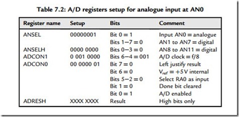
The registers used in setting up and operating the analogue input are listed in Table 7.2.

The ANSEL and ANSELH (analogue input select) register bits are configured with 0 for digital and 1 for analogue inputs. Only AN0 is required in this case (ANSEL,0), the others will be set for digital input. The register bits default to 1, or analogue inputs, so must be initialized for digital I/O with 0. Usually it is convenient to clear all the control bits, and then setthose that are required as analogue inputs.

The analogue-to-digital converter (ADC) works by a successive approximation method, and uses the system clock to drive the converter that generates the binary equivalent of the input voltage. Since the conversion takes a minimum time per bit, the clock must not be too fast, so a frequency divider is provided which can be set to a suitable value. The recommended division ratio is given in the data sheet (Table 9-1) for each oscillator frequency. In this example, a 4 MHz system clock requires division by 8, to provide a 500 kHz A/D clock. ADCON1, bits 4, 5 and 6 are used to select the recommended ADC clock rate.

ADCON0 has several functions. ADCON0,0 enables the ADC and bit 1 starts the conversion process when set to 1 in the program, and also indicates the conversion is finished when it is cleared in hardware. In the test program, this bit is polled in a loop that repeats until it is cleared. Bits 2e5 select the current input as the corresponding binary number (0000 ¼ AN0,

PIC Microcontrollers-1225

The ADC needs a reference voltage to set the range of the input that will be converted. ANCON0,6 selects between an internal reference of 5 V and an external reference which must be supplied from a constant voltage circuit, usually based on a zener diode. A 10-bit conversion gives results from 0000000000 (010) to 1111111111 (102310) or 1024 steps, giving a resolution of better than 0.1%. If an accurate reference voltage of say 4.096 V is supplied, the resolution will be 4096/1024 ¼ 4.00 mV per bit. With a 5 V reference, the resolution would not be such a convenient value (5000/1024 ¼ 4.88 mV), but no external circuit is needed. In the test program, an accurate measurement is not needed, so the internal reference is used.

Since the result is more than 8 bits, two registers are needed to receive the result: ADRESH and ADRESL. The justification of the result controls how it is placed in these. Left justification places the high 8 bits in ADRESH and the low 2 bits in ADRESL (bits 6 and 7). In the test program, therefore, the whole range is covered (0e5 V) by reading ADRESH, but at reduced 8-bit resolution (19.5 mV per bit). Right justification places the low 8 bits in ADRESL, providing 25% of the range (0e1.25 V) but at full resolution.


PIC Development Systems:In-Circuit Debugging

In-Circuit Debugging

In-circuit debugging (ICD) is the most powerful fault-finding technique available for microcontrollers. It allows the chip to be programmed and tested in circuit using the standard MPLAB debugging tools to control program execution in the actual target board. This is obviously a major advantage, as it allows the interaction of the PIC chip with the real hardware to be more fully examined than in a purely software simulation. Microchip currently offers three main debugging interfaces, of increasing cost and power, which all support the whole range of PIC chips. These are:

• PICkit3

• ICD3

• Real ICE.

They all possess the following features:

• USB connection

• Program download, read and verify

• In-circuit debugging, including

• Unconditional and conditional breakpoints

• Register display and stopwatch timing.

PICkit3 is the most cost-effective solution for non-professional developers, providing all the necessary features for learning and hobby applications in a compact and easy-to-use package. It is an enhanced version of PICkit2, operating at a USB full speed data rate of 12 Mb/ s. It uses the six-pin in-line board connector, which will normally connect direct to the chip in circuit.

ICD3 is more powerful, operating with high-speed USB (up to 480 Mb/s) to provide real-time ICD with maximum MCU clock rates and more complex breakpoint triggering options. It uses the six-pin RJ-11 connector, designed to connect directly to chips that support ICD, or to a header board (see below) for those that do not.

PIC Microcontrollers-1228

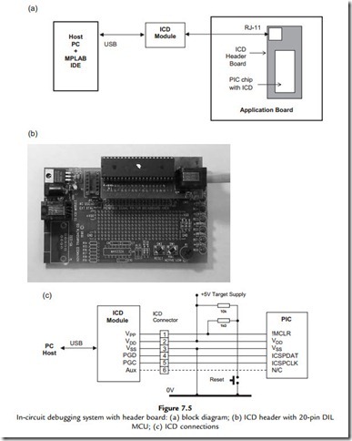
PICkitX and ICDX programmers are both capable of supporting ICD. Unfortunately, the smaller mid-range (16FXXX) chips, including the 16F690 chip fitted in the LPC board, do not support ICD internally, owing to pin-out limitations and cost constraints. For these chips, ICD can be implemented instead by using a header board connected between the ICD module and the chip socket on the application board. The header board carries a version of the target chip that incorporates the on-chip ICD circuitry, which substitutes for the target device while the system is under development (these chips are not available separately).

The ICD header system configuration is shown in Figure 7.5(a). The ICD module sits in between the host PC running MPLAB IDE and the application board MCU socket (Figure 7.5b). When debugging is complete, the chip can be programmed to run independently and plugged directly into the board. The ICD signals are shown in Figure 7.5(c), with definitions provided in Table 7.1. The on-board reset circuit has been included to show how it is isolated from the VPP by a 1k0 resistor.


PIC Development Systems:In-Circuit Emulation

In-Circuit Emulation

An in-circuit emulator (ICE) traditionally allows processor systems to be tested without the microcontroller or microprocessor present. A host computer with a hardware dedicated emulator pod replaces the target processor, with a header connector with the same pin out as the processor connected to its socket on the application board. The emulator then substitutes for the processor operating at full speed with the real hardware, giving complete control

over the target system. In the microcontroller, however, only the ports are accessible on the pins, so internal debug circuitry is needed to feed register status information out to the debugger in real time, or a header is needed to substitute for the MCU and generate the same data.

The Microchip REAL ICE debugger offers the most comprehensive facilities of the range of in-circuit programmer/debuggers, with multiple modes of operation for interactive hardware testing. As well as the standard connections to the target, or substitute header board, high-speed options are available which can also employ the serial and parallel ports to supply additional debug information. PIC 32 devices have special trace outputs to enhance the debugging operation.

For professional development, the PIC REAL ICE provides superior performance and additional debug facilities, while using the same programming and debugging connections in the target device. For programming chips on a commercial scale, the Microchip PM3 and a number of third-party programmers are available. For current product information, visit www.microchip.com.

1. List the functions of pins 1e5 on the six-pin programming connector of the PICkit2 module. (5)

2. A PIC 16F690 is to be used for digital input on all pins of port C, and therefore no port initialization is performed. Why will this not work correctly? (2)

3. Calculate the maximum value and resolution of an A/D conversion if the reference voltage is 1.024 V, the result is right justified and only the contents of ADRESL are used. (4)

4. Explain why testing a program in simulation mode speeds up the development process. (3)

5. Why does the push button on the LPC board not work when the board is attached to the PICkit2 programmer? (3)

6. Compare the Microchip LPC board with the 44-pin demo board and summarize the additional features of the latter.

1. Download the program LPC1.ASM from the support website www.picmicros.org.uk, load it into MPLAB, assemble and test it in MPLAB. Ensure that the output port bit rotates as required. Modify the program so that the delay count is fixed at 0x80, and check the cycle time is about 1 s. Make sure the clock frequency is set to 4 MHz.

2. If you have access to Proteus VSM, download LPC690.DSN and test the program as above with the pot in mid-position. Setup the display as per Figure 7.4. Check that the output speed is controlled by the pot, and ADRESH and PORTB are displayed correctly.

3. Obtain the PICkit2 demo kit with LPC and test the system using the program LPC1. Connect the hardware, load the program into MPLAB, select PICkit2 programmer, download and run. The MCLR buttons should switch the sequence on and off, and the pot should control the speed.

4. Log onto www.microchip.com and research the current range of starter kits (home/ development tools/starter kits).


PIC Development Systems:Other PIC Demo Kits

Other PIC Demo Kits

There are several other Microchip demonstration kits that allow the user to investigate a range of devices and techniques and provide convenient hardware platforms for further application development. The features of some of the currently available range are summarized in Table 7.3, and described below.

44/28-Pin Demo Boards

The 44-pin demo board incorporates the 16F887 MCU, which has a full range of features in a surface-mounted TQFP package. The chip has 33 I/O pins (ports AeE), so is useful if more peripherals are needed. Additional features are a full set of eight LEDs, a 32 kHz

crystal clock input for timer 1 and a 10 MHz system crystal clock. A major advantage of the board is that the ’887 supports direct ICD (without a header). Otherwise, the board facilities are similar to the LPC demo board with a small prototyping area and extra connections to the chip. The 28-pin board has similar features, but with the smaller sibling of the ’887 chip, the 16F886, fitted.

PICDEM2 Plus Demo Board

This board has an alphanumeric liquid crystal display (LCD) commonly used to display simple messages in microcontroller applications. As well as push-button switches and a buzzer, it has a serial EEPROM that allows the I2C serial protocol to be examined, and a temperature

sensor, which can provide real-time data for storage. It has 18-, 28- and 40-pin dual in-line (DIL) sockets, allowing a range of different chips to be fitted.

PICDEM Lab Development Kit

This kit allows users to build peripheral circuits on a plug board, and is therefore a good choice for training purposes. It includes a set of different processors and a brushed direct current (dc) motor. Flowcode programming software is included, which is a user-friendly option that avoids the need to learn the details of assembler programming. Programs are entered as a flowchart (see Section 4.2 on program design in Chapter 4), which is then compiled directly to downloadable code.

PIC Microcontrollers-1227

This kit, again based on the 16F886 MCU, has a small computer fan on board, incorporating a brushless dc motor and a sensor to monitor the fan speed, allowing experimentation with closed loop motor control, as well as a heater and temperature sensor. C compilers are included, so that more complex programs can be developed, especially applications requiring real-time calculations. A serial analyzer pod also allows the communications signals produced in the board to be examined at the outputs.


PIC Development Systems:Simulation Test

Simulation Test

The program can be tested in simulation mode before downloading to the LPC board. Assuming it has been edited and assembled in MPLAB, MPSIM can be invoked and the program run with the SFRs, stopwatch, etc., displayed. However, an analogue input stimulus is not available in MPSIM, so the ADRESH must be loaded via a register stimulus or a modified simulation version of the program used where a literal is loaded in place of the input. Otherwise, the program can only then be tested with the delay count loaded with 00 from ADRESH, giving the maximum delay.

Interactive simulation using Proteus VSM (Figure 7.4) is, therefore, in this case, simpler and more convenient. The program is written, assembled and attached to the MCU in the schematic, and the simulation run with source code and SFRs displayed (see Appendix E

for tutorial notes). The pot can be adjusted on screen and the LEDs will animate in real time, so correct program function can quickly be demonstrated. The program timing can be checked on the display of simulated time elapsed in the status bar.

The advantages of both systems can be realized by running the interactive simulation from within MPLAB. The debug tools provided by MPLAB are used to control the VSM simulation in a viewing window, while the interactive features are still available.

PIC Microcontrollers-1226

The simulation test allows the basic program syntax and logic to be checked before downloading. Any syntax errors will be detected by the assembler, with a line number indicated and the error type indicated in the output window. If the scanning output is not obtained, check the main sequence by single stepping through the main loop, stepping over the delay subroutine. If the sequence appears correct, view the SFRs and check that the changes are correct. If the main sequence and intialization are correct, step into the delay loop and make sure the program is not getting stuck in an endless loop and failing to return.