Light Projects:LED Binary Counter

This chapter describes simple light projects using the basic 89C2051 micro- controller circuit described in earlier chapters. Over ten projects are given, from very simple LED display projects to complex projects incorporating alpha- numeric displays. For each project, the following information is given as appropriate:

• Function: what the project does, its inputs and outputs.

• Circuit diagram: full circuit diagram of the project and explanation of how the circuit works.

• Program description: functional description of the software in simple English-like language (PDL).

• Program listing: full tested and working C program listing for each project,

including comments.

• Components required: listing of components required to build each project.

LED Binary Counter

Function

This project counts up in binary and displays the result on eight LEDs connected to port 1 of the microcontroller as shown in Fig. 3.1.

Circuit Diagram

As shown in Fig. 3.2 the circuit is extremely simple, consisting of the basic 89C2051-based microcontroller and eight LEDs connected to port 1 of the microcontroller. Each microcontroller output pin can sink a maximum of 80 flA and source up to 20 mA. The manufacturers specify that the total source current of a port should not exceed 80 mA. There are many different types of LED lights on the market, emitting red, green, amber, white, or yellow colours. Standard red LEDs require about 5 to10 mA toemit visible bright light. There are also low-current small LEDs operating from as low as 1 mA.

Light Projects 0046

In Fig. 3.2, the microcontroller outputs operate in current source mode where an LED is turned on if the corresponding output is at logic LOW level. The required value of the current limiting resistors can be calculated as follows:

Light Projects 0047

where Vs is the supply voltage ( +5 V), Vf is the LED forward voltage drop (about 2 V), and If is the LED forward current (1 to 30 mA depending on the type of LED used). In this design if we assume an LED current of about 6 mA, the required resistors will be:

Light Projects 0048

Although eight individual resistors are shown in this circuit, it is possible to replace these resistors with a single DIL (dual-in-line) resistor chain.

Program Description

The program is required to increment a value and then output to port 1 of the microcontroller. Because the microcontroller operates at a very high speed, it is

Light Projects 0049

Light Projects 0050

Program Listing

The full program listing is shown in Fig. 3.3. Variable LED is initialized to1 and is used as the counter. The endless loop is set using the for statement with noparameters. Variable P1 is defined in include file ‘AT892051.h’ and this is a reserved name for port 1 of the microcontroller. Notice that variable LED is complemented (using operator ‘rv’) and then sent to the output port. This is necessary since the output ports are configured to source current, i.e. an LED is turned on when the corresponding port output is logic LOW. A delay of approximately 1 second is obtained by the function wait_a_second. This function is simply a dummy for loop and gives about 1 second delay when the microcontroller is operated with a 12 MHz crystal. Different values of loop

count will give different delays. Also, different delays will be obtained with other C compilers. More accurate and compiler independent delays can be obtained using the timer utilities of the microcontroller.

Components Required

In addition to the components required by the basic microcontroller circuit, the following components will be required for this project:

R2 470 0, 0.125 W resistor (8 off), or DIL package D LED (8 off)


Matrix Keypad + serial transmission

Test 15. Matrix Keypad + serial transmission

Keypads play important role in a small embedded system where human interaction or human input is needed. All we have to do is connect the rows and columns to a port of microcontroller and program the controller to read the input.

We make the rows as i/p and we drive the columns making them o/p, this whole procedure of reading the keyboard is called scanning.

A 3 x 4 matrix keypad is used for data entry. The 12 push switches are connected to seven lines of port A, as shown in figure 36.

Interfacing PIC Microcontrollers to Peripherial Devices-0372

Interfacing PIC Microcontrollers to Peripherial Devices-0373Interfacing PIC Microcontrollers to Peripherial Devices-0374Interfacing PIC Microcontrollers to Peripherial Devices-0375Interfacing PIC Microcontrollers to Peripherial Devices-0376Interfacing PIC Microcontrollers to Peripherial Devices-0377Interfacing PIC Microcontrollers to Peripherial Devices-0378Interfacing PIC Microcontrollers to Peripherial Devices-0379Interfacing PIC Microcontrollers to Peripherial Devices-0380Interfacing PIC Microcontrollers to Peripherial Devices-0381Interfacing PIC Microcontrollers to Peripherial Devices-0382Interfacing PIC Microcontrollers to Peripherial Devices-0383Interfacing PIC Microcontrollers to Peripherial Devices-0384Interfacing PIC Microcontrollers to Peripherial Devices-0385Interfacing PIC Microcontrollers to Peripherial Devices-0386Interfacing PIC Microcontrollers to Peripherial Devices-0387Interfacing PIC Microcontrollers to Peripherial Devices-0388Interfacing PIC Microcontrollers to Peripherial Devices-0389

Program description

Interrupt Service Routine has not been used in the program.

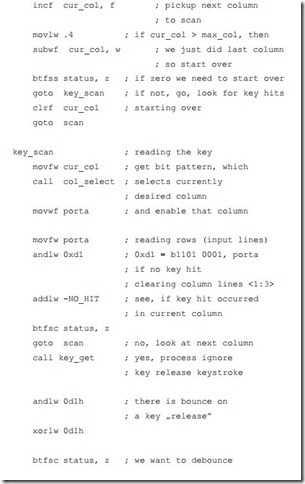
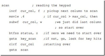
The three columns of the keypad are connected to three of the output signals from the PIC. The four rows of the keypad are connected to four of the input signals to the PIC. If no key is pressed there is no electrical contact between the rows and the columns. The PIC detects which key is pressed by ‘scanning’ the keypad.

First the PIC makes the column 1 current column and sets the signal going to Col- umn 1 low (a digital ‘0’). All the other Columns are made high (a digital ‘1’). Then it tests the input signals coming from each Row in turn. If any of the Row signals is low, this means that the corresponding key in Column 1 has been pressed. Current column number is stored to the variable cur_col.

Interrupt Service Routine has not been used in the program. During the initializa- tion phase the variable cur_col is cleared:

Interfacing PIC Microcontrollers to Peripherial Devices-0390

Interfacing PIC Microcontrollers to Peripherial Devices-0391

Now if we know valid keys, they have to be translated into ASCII codes. This task carries out the routine key_xlate. The lookup tables are built with the respective values for each column and each row. The lowest ASCII code is for the character

# (ASCII code 35)In lookup tables we assign 0 for the # character and starting with 0 we successively assign next numbers for next characters. Therefore after finishing this procedure to each value we have to add 35.

Interfacing PIC Microcontrollers to Peripherial Devices-0392

Finaly the found ASCII codes are sent to LCD for displaying and in parallel for transmission to terminal window on PC.


Dual RS232 software interface for PC and PIC microcontroller

Test 14. Dual RS232 software interface for PC and PIC microcontroller

In many PICMicros a built in serial interface, known as USART for “Universal

Synchronous/Asynchronous Receiver/Transmitter” is available. This hardware al- lows data to be received and sent without any software involvement. To send data, the USART simply shifts the data out (low byte first) to the TX I/O pin.

To receive data, the USART works by polling (sampling) the serial data input line at sixteen times the data rate. When a “low” is detected, the hardware waits 8 poll- ing cycles to check to see if the line is still low half a bit period later. If it is, then a bit is read every sixteen polling clocks until the whole byte has been read in. At the end of the byte, the Stop bit is checked to be high. If the byte is received with- out any problems, a byte received flag is set.

Interfacing PIC Microcontrollers to Peripherial Devices-0354

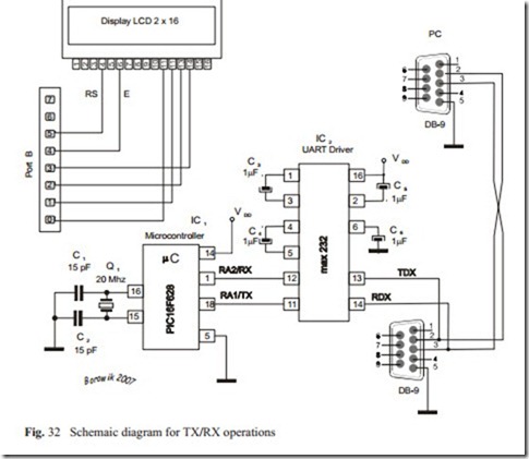
The software presented in our test provides similar serial interface functions while using not USART module, but general purpose I/O pins. This type of interfacing is known as “Bit Banging”. On the testing board serial input is connected to mi- crocontroller pin 1 (PIC16F628 RA2). Serial output is connected to microcontrol- ler pin (RA1). The Maxim “Max232” chip was used because it usesa single +5 Volt power supply. The schematic diagram is presented below.

Interfacing PIC Microcontrollers to Peripherial Devices-0355Interfacing PIC Microcontrollers to Peripherial Devices-0356Interfacing PIC Microcontrollers to Peripherial Devices-0357Interfacing PIC Microcontrollers to Peripherial Devices-0358Interfacing PIC Microcontrollers to Peripherial Devices-0359Interfacing PIC Microcontrollers to Peripherial Devices-0360Interfacing PIC Microcontrollers to Peripherial Devices-0361Interfacing PIC Microcontrollers to Peripherial Devices-0362Interfacing PIC Microcontrollers to Peripherial Devices-0363Interfacing PIC Microcontrollers to Peripherial Devices-0364Interfacing PIC Microcontrollers to Peripherial Devices-0365Interfacing PIC Microcontrollers to Peripherial Devices-0366

Program description

We use Bit-Banging method to emulate serial port. In this method we manage all synchronization and timing signals and we have to ensure proper setup and times for reading and writing data to the ports.

Bits are transfered in „8-N-1” format which means that eight data bits are sent with a single (low) Start Bit and high Stop Bit to make up a data packet. “8-N-1 is a simple and convenient protocol. The packet ends with a “1” being sent as a Stop Bit, to allow the “0” Start Bit to be easily recognised. In the idle state the line is on high. N letter means that no parity checking is performed.

Each bit is transmitted for a set period of time, the reciprocal of which is the “data rate”. Common data rates are 300, 1200, 2400, 9600, 19200 bps. As equipment

got faster, the data rates became multiples of these speeds. For the rate 9600 bps the bit time is:

1/9 600 = 104.1 μs

In our experiment we use the slow transmission: 110 bps. For this rate the bit time is:

1/110 = 9.09 ms

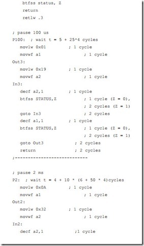
The signal for each bit, whether 1 or 0, has to stay on the transmit line over the time of app. 9.09 ms. We achieve this delay adding up: 2ms+ 2ms + 5ms + 50 μs

= 9.05 ms. The least significant bit is sent first, immediately after the start bit that is always low (0).

The start bit is an initial zero bit and the stop bit is a trailing one bit. The binary code b’01000001’ (code of the character ‘A’) is actually transmitted as follows: first the start bit 0, then 8 bits in reversed order and the stop bit high: : -> 0,0,1,0,1,0,0,1,0,1 with the start and stop bits added and the least significant bit sent first. The signal line idles at a ‘1’ (high) normally so the start bit is a change from idle to a 0 and the stop it continues at a one.

It is good custom to end the tranmission with 2 stop bits (8N2), while perform re- ception with the format 8N1. It provides some synchronization between TX and RX, assuming approximations in the delay procedures. Also between bytes we en- tered longer delays for the demo purposes.

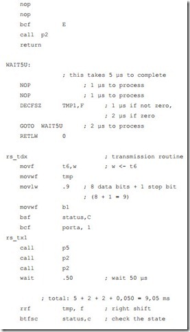
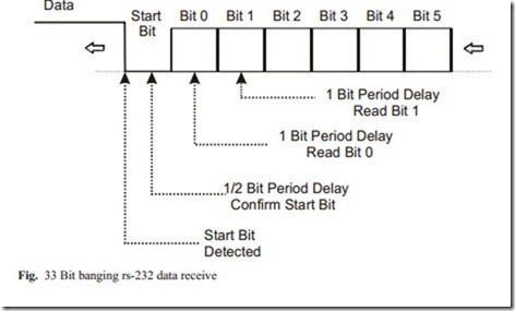
To receive data, the input line is continuously polled. When the leading edge of the start bit is detected, a half bit delay is made:

9,09/2 = 4,5 ms.

and the input line is polled again 8 times with time intervals 9.09 ms after each poll. At the end of the packet the Stop Bit is checked and the routine returns to its caller with the received byte.

Interfacing PIC Microcontrollers to Peripherial Devices-0367

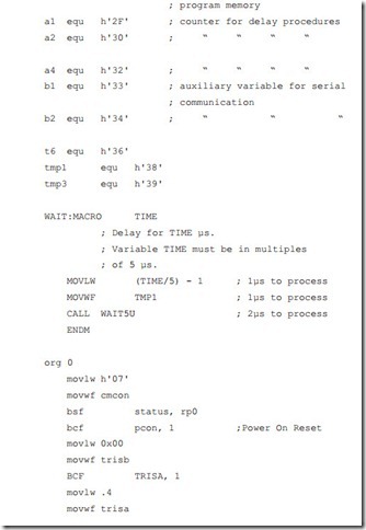
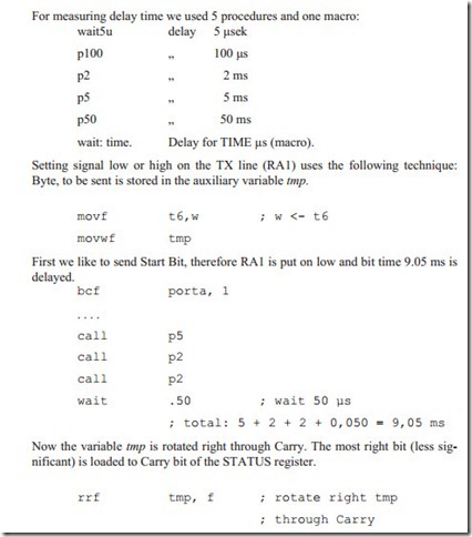
For measuring delay time we used 5 procedures and one macro:

Interfacing PIC Microcontrollers to Peripherial Devices-0368

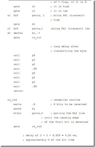
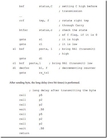
Then the state of C flag is checked. If it is high, the line RA1 is set high too. If C flag is low, RA1 is brought to low. Finaly the delay 9.05 ms is performed. This procedure is repeated 9 times (counter b1), so, that the whole byte and stop bit are outputed. Last bit sent is ‘1’, because before transmission the C Flag was set.

Interfacing PIC Microcontrollers to Peripherial Devices-0369

Interfacing PIC Microcontrollers to Peripherial Devices-0370

Receiving data is carried out in the similar manner (procedure rs_rxd).

The state if RA2 line is checked. If it is high, Carry flag is set high. If RA2 is low, the Carry Flag is brought low too. Then the auxiliary variable tmp is rotated right through Carry, loading with received bits.

Interfacing PIC Microcontrollers to Peripherial Devices-0371

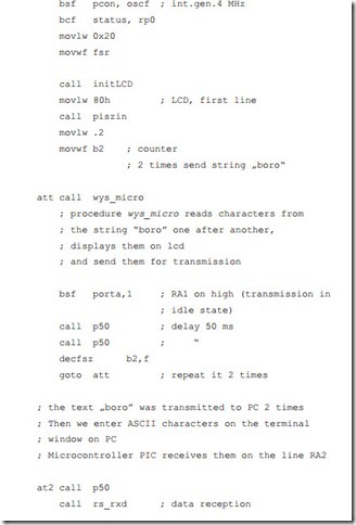
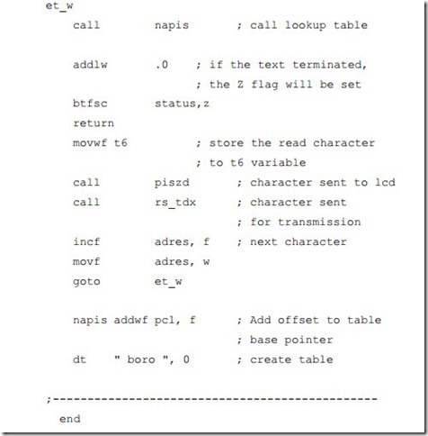
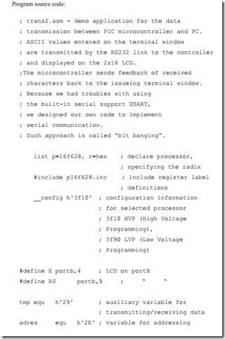
Above presented application makes first reading the text ‘boro from the lookup table. Text is 2 times written to lcd and transmitted to terminal window on PC. It can be Microsoft HyperTerminal application, but we would recommend application Tera Term Pro because of its simplicity.

After displaying on the terminal window the text: boro boro, the transmission from the PIC microcontroller is terminated and the microcontroller waits for data from PC. ASCII values entered on the terminal window are transmitted by the RS232 link to the controller and displayed on the LCD. The microcontroller sends feedback of received characters back to the issueing terminal window.


Interfacing a PIC microcontroller to an LCD Hitachi Display.

Test 12. Interfacing a PIC microcontroller to an LCD Hitachi Display.

We used an LCD 2x 16 HMC 16225 S-PY alphanumeric display module that is HD44780 compatible. Display has two lines, 16 characters each.

Interfacing PIC Microcontrollers to Peripherial Devices-0318

Low nibble of the port B: lines PORTB <3:0> communicate with DB7(pin 14) : DB4 (pin 11) of the LCD Display. LCD control signals E (Enable) and RS (Register Select) are connected to the RB4 and RB5 microcontroller PORTB lines respectively.

In 4-bit mode, two transfers per character / command are required. Half of the byte is sent in one operation, upper nibble first.

LCD’s (drivers) are slow devices when compared to microcontrollers. Care must be taken from having communication occur too quickly. The software will need to control communicaton speed and timing to ensure the slow LCD and fast micro- controller can stay synchronized.

B. Borowik, Interfacing PIC Microcontrollers to Peripherial Devices, Intelligent Systems, 56

Control and Automation: Science and Engineering 49, DOI 10.1007/978-94-007-1119-8_12,

© Springer Science+Business Media B.V. 2011

When we start to communicate with the LCD module, we follow a standard LCD initialization sequence as recommended by the manufacturer. The initialization sequence must be timed precisely (see the HD44780 instruction set for details) and cannot be initiated before at least 30 ms have been granted to the LCD module to proceed with its own internal initialization (power on reset) sequence.

Interfacing PIC Microcontrollers to Peripherial Devices-0319

When the module powers up, the default data transfer mode is 8-bit. The initializa- tion sequence only requires commands that are 4-bit in length. The last initialization command needs to specify the data transfer width (4-or 8-bit). Then a delay of 4.6 ms must be executed before the LCD module can be initialized.

Interfacing PIC Microcontrollers to Peripherial Devices-0320

Interfacing PIC Microcontrollers to Peripherial Devices-0321

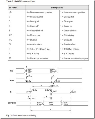
The LCD controller needs 40 to 120 microseconds (uS) for writing and reading. Other operations can take up to 5 mS. During that time, the microcontroller can not access the LCD, so a program needs to know when the LCD is busy. We can solve this in two ways.

One way is to check the LCD status register BUSY bit (BF flag) found on data line D7 (LCD pin 14). When it is low, data is written to LCD, the LCD is ready for next operation. When it is high, operation is in progress and we have to wait. On the testing board MICROCON4, R/W line is grounded and always in low therefore reaing from the LCD module status-register is disabled.

The other way to ensure, LCD is not busy, is to introduce a delays in the program. The delays have to be long enough for the LCD to finish the operation in process. The practice shows, that following delays are needed for LCD operations:

Interfacing PIC Microcontrollers to Peripherial Devices-0322

When the LCD is initialized, it is ready to continue receiving data or instructions. If it receives a character, it will write it on the display and move the cursor one space to the right. The Cursor marks the next location where a character will be written. When we want to write a string of characters, first we need to set up the starting address, and then send one character at a time.

Interfacing PIC Microcontrollers to Peripherial Devices-0323Interfacing PIC Microcontrollers to Peripherial Devices-0324Interfacing PIC Microcontrollers to Peripherial Devices-0325Interfacing PIC Microcontrollers to Peripherial Devices-0326Interfacing PIC Microcontrollers to Peripherial Devices-0327Interfacing PIC Microcontrollers to Peripherial Devices-0328Interfacing PIC Microcontrollers to Peripherial Devices-0329Interfacing PIC Microcontrollers to Peripherial Devices-0330

Interfacing PIC Microcontrollers to Peripherial Devices-0331

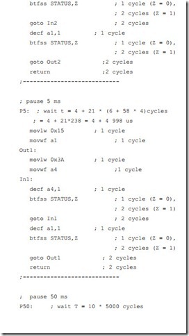
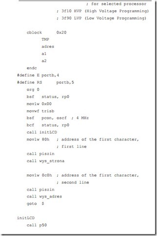
Before we can use initLCD, the delay procedures p50 (50 ms delay), p5 (5 ms delay) and p100 (100 us delay) must be defined. Also initLCD uses procedure for sending command to LCD: piszin. This procedure will be described later.

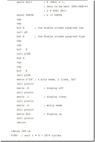
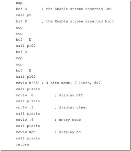
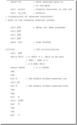
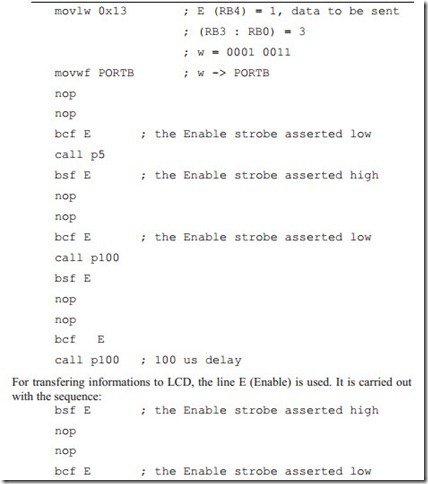
At the beginning initLCD procedure manually sends 3 times to LCD the value of 3 contained in the lower nibble of port B. Transfer is through raising and lowering the Enable strobe line.:

initLCD

call p50 ; 50 ms delay
Interfacing PIC Microcontrollers to Peripherial Devices-0332

Raising and lowering voltage on the line is called strobe. It activates information transfer. Both the data and control lines are on the same port: port B, therefore care has to be taken, that line E is on the low state, otherwise any unwanted in- formation can be sent to LCD. Usualy most of operation is performed on the working register W and, when the byte is ready to sent, it is splited into 2 nibbles, they are one after another moved to low 4 lines of port B and then the strobe sig- nal is generated.

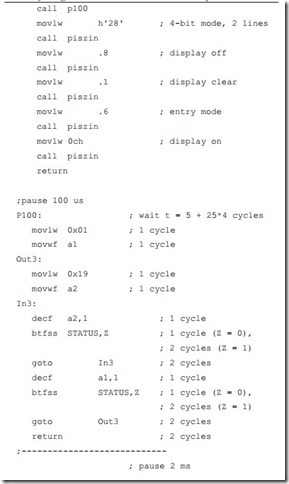
Next initialization sequence: sending commands: 0x28, 0x08, 0x01, 0x06 and 0x0c is implemented with the transfer procedure piszin, as shown below:

Interfacing PIC Microcontrollers to Peripherial Devices-0333

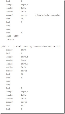
Executing each command requires at least 1.6 ms. We provide after each transfer the 2 ms delay. The respective call (call p2) is included in the piszin procedure. The description of the piszin procedure, for transferring commands to LCD:

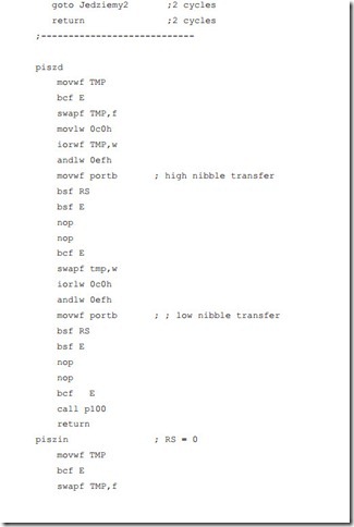
Interfacing PIC Microcontrollers to Peripherial Devices-0334

Before calling piszin, the byte to be sent is loaded to the working register W.

The LCD controller contains two separately addressable 8-bit registers: one for ASCII data and one for commands. LCD has an address line, RS, for the register selection. Its settings have the following meaning:

Register Select Control RS:

Interfacing PIC Microcontrollers to Peripherial Devices-0335

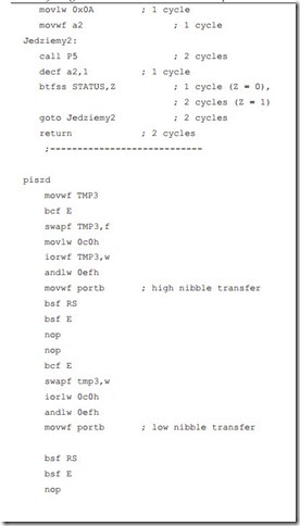
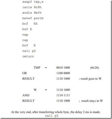
The byte to be sent has two nibbles. We have to send higher nibble first. Send operation is made on the lower 4 lines of PORTB. Therefore the byte has to be swaped and its higher part is on the lower position. Next we have to clear bits 4th and 5th, so that lines RB4 (E signal) and RB5 (RS line) of port B will be cleared. We do this with or and and operations (commands: iorwf and andlw).

Interfacing PIC Microcontrollers to Peripherial Devices-0336

Example:

If we are to send command byte 0x28, we first load the value to variable register TMP. After swapf operation, TMP register will contain 0x82, binary b’1000 0010’. We have to make sure, that line 4 (Enable) is zero. Therefore we perform inclusive or operation of this value with the mask b’1100 0000’, so that bits 6 and 7 are set, and lower bits are preserved without changes. Then we make and opera- tion with the mask: b’1110 1111’ and bit 4th is cleared. This looks as follows:

Interfacing PIC Microcontrollers to Peripherial Devices-0337

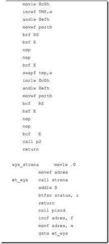
Now it is time to send next nibble. TMP register is swapped again. After iorlw and andlw operations with tha same masks result is moved to PORTB:
Interfacing PIC Microcontrollers to Peripherial Devices-0338

After initialising LCD we have to address upper or lower line of LCD. LCD controller recognizes address command, if the MSB is set. Therefore the addres of the beginning of the upper LCD line would be not 0x00, but 0x80, binary 1 0 0 0 0 0 0 0. For the lower line addres starts with 0x40. After seting the MSB it would be in hex: 0xC0, binary 1100 0000.

Because those addresses are commands, RS line has to be held low.

Interfacing PIC Microcontrollers to Peripherial Devices-0339clip_image001[16]We like to display in the upper line the string : borowik.pl. We generate this string and store in the memory with the procedure wys_strona.

Interfacing PIC Microcontrollers to Peripherial Devices-0340

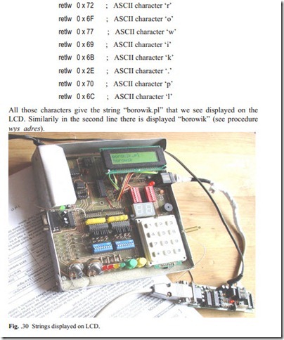
In the above procedures we form a lookup table. First we load 0 to the working register W and to the variable address. Then we call the one line procedure strona. Contents of W is table offset value. It is added to the Program Counter. Upon return W contains one by one all characters from the string. String is null terminated and after each return (retlw) contents of W is checked, if it is zero. If zero, procedure wys_strona ends. If not zero, character is sent to LCD in the pro- cedure piszd, variable address determining table offset is incremented, is moved to W and again is called procedure strona.

dt directive (Define Table) generates a series of RETLW instructions, one in- struction for each character in the string. Each character in a string is stored in its own RETLW instruction. This directive is used when generating a table of data for the PIC12/16 device family. If we were using a PIC18 device, it is recommended that we use the table read/write (TBLRD/TBLWT) features instead. Let us again consider one line procedure strona

Interfacing PIC Microcontrollers to Peripherial Devices-0341

Interfacing PIC Microcontrollers to Peripherial Devices-0342

All those characters give the string “borowik.pl” that we see displayed on the LCD. Similarily in the second line there is displayed “borowik” (see procedure wys_adres).

Procedure piszin, described earlier sends commands to the LCD controller. Procedure piszd for sending data (ASCII characters) to LCD is similar. The only differ- ence is, that the RS (Register Select) line must be set high.


Timer

Test 13. Timer

Real Time Clock emulation on the LCD Source code:

Interfacing PIC Microcontrollers to Peripherial Devices-0343Interfacing PIC Microcontrollers to Peripherial Devices-0344Interfacing PIC Microcontrollers to Peripherial Devices-0345Interfacing PIC Microcontrollers to Peripherial Devices-0346Interfacing PIC Microcontrollers to Peripherial Devices-0347Interfacing PIC Microcontrollers to Peripherial Devices-0348Interfacing PIC Microcontrollers to Peripherial Devices-0349Interfacing PIC Microcontrollers to Peripherial Devices-0350Interfacing PIC Microcontrollers to Peripherial Devices-0351Interfacing PIC Microcontrollers to Peripherial Devices-0352

Program description

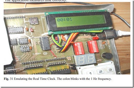
When microcotroller powers on, it starts counting the time and shows the time on the LCD display in the format HH:MM. Colon between hours and minutes is flickering with the frequency of 1 Hz. After 60 s number of minutes increases with

1. When the number of minutes reaches 10, it is cleared and tne number of tens of minutes is increased. When it reaches 6 (when it is 60 minutes), the number of hours increases and number of minutes is cleared and so on. Detailed explanation is in comment lines.

The application measures time correctly.

Interfacing PIC Microcontrollers to Peripherial Devices-0353


Driving a 7-Segment LED Display with PIC16F628 microcontroller (cont.)

Test 11. Driving a 7-Segment LED Display with PIC16F628 microcontroller (cont.)

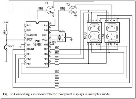
Our board is containing a dual 7 segment LED display. The display is a common catode type, so to light a segment we need to take the relevant segment high and the common cathode must be connected to the 0V rail. In order to reduce the I/O count we’re multiplexing the display digits.

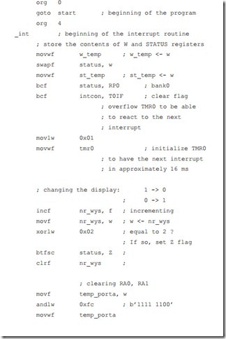
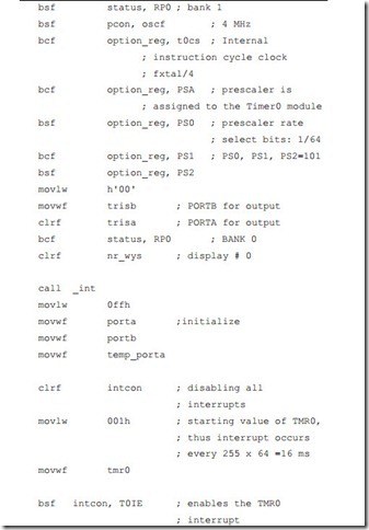
Program prints two digits: ‘0 1’ on two 7seg displays in multiplex mode. Displays are multiplexed with a frequency of 61 Hz:

T multipl. = 1 us * 64 (prescaler) * 256 (counter) = 16 384 1/T = appr. 61 Hz

Interfacing PIC Microcontrollers to Peripherial Devices-0304Interfacing PIC Microcontrollers to Peripherial Devices-0305Interfacing PIC Microcontrollers to Peripherial Devices-0306Interfacing PIC Microcontrollers to Peripherial Devices-0307Interfacing PIC Microcontrollers to Peripherial Devices-0308Interfacing PIC Microcontrollers to Peripherial Devices-0309

Each display is turned on at a such rate, that persistence of vision of our eye thinks the display is turned on the whole time. As each display is turned on, the appropriate information must be delivered to it so that it will give the correct read- ing. Therefore, the program has to ensure the proper timing, else the unpleasant blinking of display will occur.

Displaying digits is carried out in multiplex mode which means that the microcontroller alternately prints on first and on the second display. TMR0 interrupt serves for generating a time period, so that the program enters the interrupt routine every 16 ms and performs multiplexing. In the interrupt routine, first step is deciding which segment display should be turned on. In case that the first display was pre- viously on, it should be turned off, set the mask for printing the digit on next 7seg display which lasts 16 ms, i.e. until the next interrupt.

Operating the device is fairly straight forward. By selectively connecting a digit- select line (one of the 2 common cathodes) to ground and applying a positive volt- age to any of the segment-select lines (common anode), it is possible to illuminate any segment of any digit. Port B on the PIC16F628 is 8 bits wide: one bit for each segment.

Interfacing PIC Microcontrollers to Peripherial Devices-0310

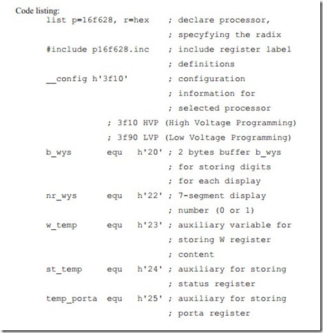
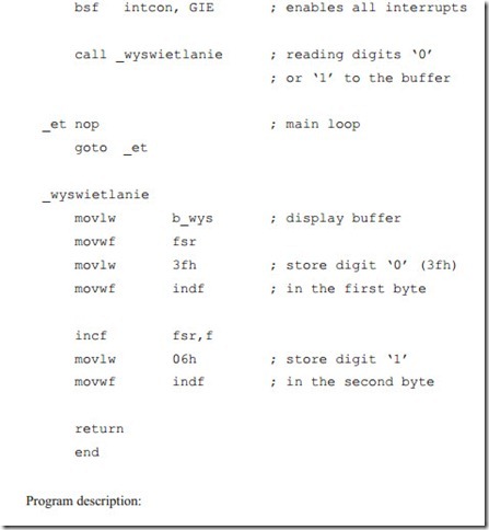
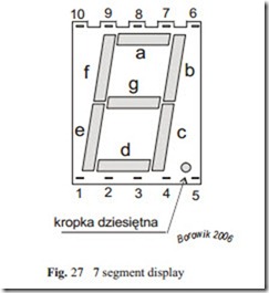
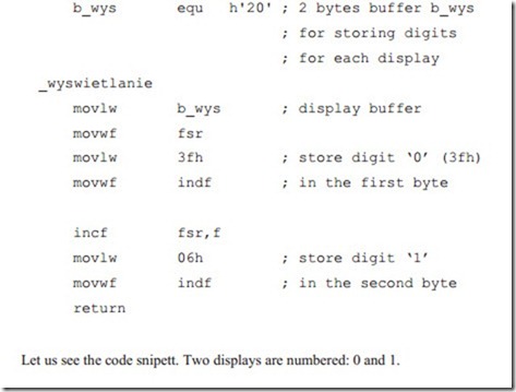
For displaying digit ‘0’ we have to turn on the following segments of the display: a, b, c, d, e, f. Into port B we have to put the value binary: b’00111111’, hexa- decimaly: 0x3f.

For displaying digit ‘1’ we have to turn on the segments b and c. Into port B we have to put the value binary: b’00000110’, hexadecimaly: 0x06.

Both values in the routine _wyswietlanie we put into RAM memory to the

variable b_wys, denoting the display buffer.

Interfacing PIC Microcontrollers to Peripherial Devices-0311

Interfacing PIC Microcontrollers to Peripherial Devices-0312

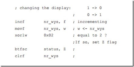
After incrementing display # 0 becomes # 1. That is OK.

Incrementing display number 1 gives #2. We detect this by xoring nr_wys (display #) with the value of 2 (0x02). Then we clear it, so display # 1 becomes # 0.

Interfacing PIC Microcontrollers to Peripherial Devices-0313

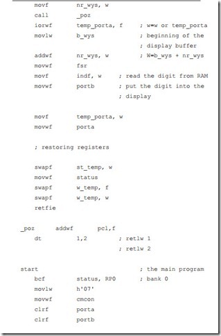
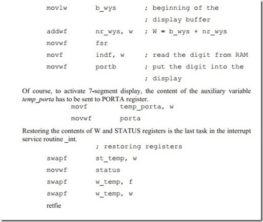
We put to ground common cathodes of both displays, and save this setting to aux- iliary variable temp_porta.. Now we have to send the appropriate digit pattern to port B. Both digit patterns are stored in RAM memory in the INDF register. The first digit: 0 (the pattern is 3fh or b’0011 1111’) has the memory address h20. The next digit: 1 (the pattern 06h or b’0000 0110’) occupies the next memory location.

Interfacing PIC Microcontrollers to Peripherial Devices-0314

In above two lines we load the display # into W register. Then we call subroutine _poz. If the display # was 0, we receive in W on return value of 1. If the display # was 1, we receive in W on return value of 2.

Interfacing PIC Microcontrollers to Peripherial Devices-0315

This value in W register is then ored with temp_porta register in order to turn off one of two 7-segment displays. If the W register was 1, the RA0 receives value of 1, turning the attached to it 7-segment display off. If the W register was 2, the RA1 receives value of 1, turning the attached to it 7-segment display off.

Interfacing PIC Microcontrollers to Peripherial Devices-0316

Then the address in RAM memory of the digit pattern to be displayed is com- posed. To the address of the display buffer b_wys, which is 0x20 we add the dis- play #, which is 0 or 1. Thus W now points to the digit pattern of ‘0’ (0x3F) or to the digit pattern of ‘1’ (0x06). Contents of W register is then moved to the File Se- lect Register and appropriate digit pattern can be read from the indf register. Ob- tained digit pattern is next put into port B.

Interfacing PIC Microcontrollers to Peripherial Devices-0317


Driving a 7-Segment LED Display with PIC16F628 microcontroller

Test 10. Driving a 7-Segment LED Display with PIC16F628 microcontroller

Below presented application was run on the prototype board Microcon4. The application can be used for testing all 8 lines connecting port B with the display and the display itself. 16 hexadecimal digits 0 – F are shown sequentialy one after an- other with time span 0.9s each.
Interfacing PIC Microcontrollers to Peripherial Devices-0294

B. Borowik, Interfacing PIC Microcontrollers to Peripherial Devices, Intelligent Systems, 39
Control and Automation: Science and Engineering 49, DOI 10.1007/978-94-007-1119-8_10,

Interfacing PIC Microcontrollers to Peripherial Devices-0295

The circuit is very simple. Port A, bits 0-4 are connected to the digit select lines directly. Port B, bits 0-7 are connected to the segment select lines through 330 Ω resistors. A 4MHz crystal resonator is connected to the OSC1/CLKIN and OSC2/CLKOUT pins of the PIC, with the center lead connected to Gnd. Vss and Vdd are connected to Gnd and +5V, respectively.

Interfacing PIC Microcontrollers to Peripherial Devices-0296Interfacing PIC Microcontrollers to Peripherial Devices-0297Interfacing PIC Microcontrollers to Peripherial Devices-0298Interfacing PIC Microcontrollers to Peripherial Devices-0299Interfacing PIC Microcontrollers to Peripherial Devices-0300

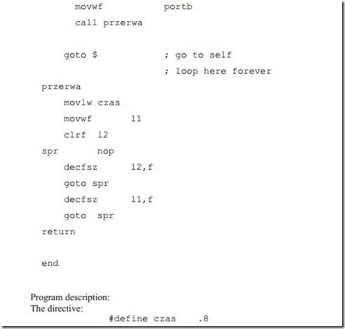
defines value of 8 decimal for register variable czas.

In the MPASM assembler (the assembler) that provides a platform for developing assembly language code for Microchip’s PICmicro microcontroller (MCU) fami- lies, a decimal integer is `d’ or `D’ followed by one or more decimal digits `0123456789′ in single quotes, or, a decimal integer is `.’ followed by one or more decimal digits `0123456789′.

The directives:

Interfacing PIC Microcontrollers to Peripherial Devices-0301

are used to assign a variable names l1 and l2 to an address locations in RAM re- spectively h’20’ and h’21’.

Routine przerwa contains nested loop. Two general purpose registers l2 and l1 are decremented. l2 is first cleared and then is decremented in the inner loop with in- struction decfsz (decrement f, skip if zero). The loop is executed 256 times. It takes time of 110.592ms (256 x 4 x 108us).

4 accounts for 4 machine cycles:

Interfacing PIC Microcontrollers to Peripherial Devices-0302Nop instruction adds up to the number of machine cycles in one iteration.

The segments in a 7-segment display are arranged to form a single digit from 0 to F as shown in the figure:

Interfacing PIC Microcontrollers to Peripherial Devices-0303

Segments 0 to 7 are marked respectively with non-capital letters: a, b, c, d, e, f, g and dp, where dp is the decimal point. The 8 display segments lines (0 to 7) are connected to the 8 PortB lines. PORTB is made output by clearing TRISB regis- ter.

In order to reduce the number of pins in the device, a clever arrangement of com- mon cathode is employed. Since there are 8 segments (7 plus the decimal point), there are 8 anode connections. Onto the PORTB are put respective values, repre- senting particular digits from 0 to F and at the last: the decimal point. Those val- ues were defined at the beginning of the program.

Value 1 means the respective LED segment is turned on. To display 8 we need to put a binary b’01111111′ on PortB. This will turn on all the LEDs except the decimal point. The number 0 is simply an 8 with the middle segment off, b’00111111′. The decimal point has its value: b’10000000’.


Working with debugger. Turn the LED on for the calculated period of time.

Test 9. Working with debugger. Turn the LED on for the calculated period of time.

Interfacing PIC Microcontrollers to Peripherial Devices-0280Interfacing PIC Microcontrollers to Peripherial Devices-0281

We select Debugger>Select Tool pull down menu and check MPLAB SIM. Addi- tional menu items will appear in the Debugger menu.

The MPLAB SIM simulator is integrated into MPLAB IDE integrated develop- ment environment.

MPLAB SIM allows us to:

· Modify object code and immediately re-execute it

· Trace the execution of the object code

The simulator is a software model, and not actual device hardware.

When MPLAB SIM is simulating running in real time, instructions are executing as quickly as the PC’s CPU will allow. This is usually slower than the actual de- vice would run at its rated clock speed.

The speed at which the simulator runs depends on the speed of our computer and how many other tasks we have running in the background.

Once we have chosen a debug tool, we will see changes in the following on the IDE:

1. The status bar on the bottom of the MPLAB IDE window should change to "MPLAB SIM".

2. Additional menu items should now appear in the Debugger menu.

3. Additional toolbar icons should appear in the Debug Tool Bar. After position- ing the mouse cursor over a toolbar button, a brief description of the button’s function can be seen.

4. An MPLAB SIM tab is added to the Output window.

Interfacing PIC Microcontrollers to Peripherial Devices-0282Interfacing PIC Microcontrollers to Peripherial Devices-0283

After positioning the mouse cursor over a toolbar button we can see a brief de- scription of the button’s function.

Interfacing PIC Microcontrollers to Peripherial Devices-0284

Standard debug windows allow to view the actual code, as well as the contents of program or data memory. The watch window displays the values of registers that are specified.

Next we select Debugger -> Reset -> Processor Reset and a green arrow shows where the program will begin (see Fig. 14). In our project it is the line:

Interfacing PIC Microcontrollers to Peripherial Devices-0285

which is loading working register with the value of 7.

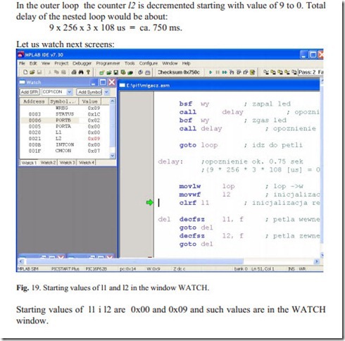
In order to see if the code is operating as intended, we can watch the values being changed in the program. Selecting View>Watch brings up an empty Watch win- dow. There are two pull downs on the top of the Watch window. The one on the left labeled "Add SFR" can be used to add the Special Function Registers into the watch. We select from the list following Special Function Registers: WREG, STATUS, PORTB, PORTA, INTCON, CMCON and sequentially after each se- lection we have to click Add SFR to add respective register each of them to the window.
The pull down on the right, allows symbols to be added from the program. We use this pull down to add two our variables: l1 and l2 into the Watch window. We se- lect them from the list and then click Add Symbol to add them to the window. The Watch window should now show the address, value and name of the selected registers.

To single step through the application program, we select Debugger>Step Into or click the equivalent toolbar icon. This will execute the currently indicated line of

code and move the arrow to the next line of code to be executed. After repeating twice Step Into the value of 7 will be moved from WREG register into SFR CMCON.

Interfacing PIC Microcontrollers to Peripherial Devices-0286

The value of CMCON register in the Watch window is in red color because it was changed by the previous debug operation, values that were not changed are black.

We can continue single stepping through the code. Next instructions are: clearing registers PORTA and PORTB and clearing RBIE bit of the INTCON register. Clearing the RBIE mask disables interrupt-on-change feature of PORTB. Then we will set RP0 bit of STATUS register for selecting data memory bank 1 as is shown in figure 16.

Interfacing PIC Microcontrollers to Peripherial Devices-0287

Interfacing PIC Microcontrollers to Peripherial Devices-0288Interfacing PIC Microcontrollers to Peripherial Devices-0289Interfacing PIC Microcontrollers to Peripherial Devices-0290Interfacing PIC Microcontrollers to Peripherial Devices-0291

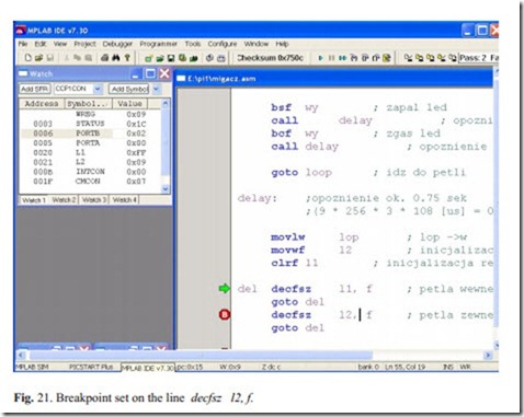
Instead of continuing single stepping through the code and executing thousands of steps, it is better to set a breakpoint on the selected line and run the code. To set a breakpoint, we can put the cursor on the selected line and click the right mouse button. Then select Set Breakpoint from the context menu. A red "B" will show on the line. (One can also double click on a line to add a breakpoint.)

On the figure below Breakpoint is set at the line, where l2 variable is decremented and tested., after inner loop has been executed 256 times.

We can enter Run mode by either clicking the Run button on the Debug toolbar, selecting Debugger>Run from the menu bar, or pressing <F9> on the keyboard. Some tools provide additional types of run, such as "Run to cursor" from the right- mouse menu.

Interfacing PIC Microcontrollers to Peripherial Devices-0292

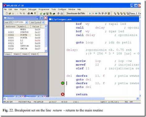
After running application the program code is executed until a breakpoint is en- countered. In the outer loop we decrement the variable l2. Next breakpoint should be set on the instruction return, in order to exit the subroutine del and return to main routine.

Interfacing PIC Microcontrollers to Peripherial Devices-0293


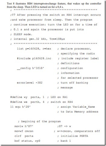
Waking the device from SLEEP with RB4 interrupt-on- change

Test 8. Waking the device from SLEEP with RB4 interrupt-on- change

Interfacing PIC Microcontrollers to Peripherial Devices-0275Interfacing PIC Microcontrollers to Peripherial Devices-0276

Interfacing PIC Microcontrollers to Peripherial Devices-0277

Program description

Four PORTB pins, RB<7:4>, if configured as inputs, have an interrupt-on-change feature. This interrupt sets flag bit RBIF and can wake the device from SLEEP. Interrupt is enabled after setting the RBIE mask:

bsf intcon, rbie

Interrupt on mismatch feature together with software configurable pull-upps on these pins allow easy interface to a switch and make it possible for wake up on switch depression.

Interfacing PIC Microcontrollers to Peripherial Devices-0278

After sleep instruction the device enters the sleep mode and waits for interrupt to be waked up.

If the interrupt is enabled by the associated Interrupt mask IE and the GIE bit is not set, it can wake up the controller from the sleep if interrupt occurs, but the Interrupt Service Routine located in the interrupt vector will not be executed and the code of the program will continue execution. The interrupt flag will set when its associate event occurs regardless of whether or not the GIE bit is set.

After switch is released, the RBIF flag is cleared and the device again is put to the sleep mode at the beginning of the loop..

Interfacing PIC Microcontrollers to Peripherial Devices-0279