Logic Gate Input and Output
If you have worked with digital electronics before, you probably have made a few assumptions about how the circuitry works and how you can demonstrate how digital electronic devices work. Chances are many of these assumptions are with regard to how gate and chip inputs and outputs work as well as how to properly interface them together and to different electronic devices. These assumptions are generally made on the evidence of by what somebody has seen with a voltmeter or logic probe and do not look at the underlying circuitry and how it works. In this section, I will give you a detailed introduction to the input and output pins on digital electronics and how they should be wired.
When we talk about digital electronics, we should identify the different technologies used. ‘‘Transistor to transistor logic’’ (TTL) is based on NPN bipolar transistors. TTL chips have the part number prefix ‘‘74’’ (i.e. a chip with four, two input NAND gates known as the ‘‘7400’’). There are actually quite a few different technology chip families based on the 74xx ‘‘standard’’
pinout and operation and the technology is indicated by letter codes following the ‘‘74’’; a chip marked with ‘‘74LS00’’ is a low-power, Shotkey four two-input NAND gate chips. Many of these technologies used with the 7400 series of chips are based on bipolar transistors, but some are based on MOSFET technology. These MOSFET technology based chips have the 74 prefix and a technology letter code containing a ‘‘C’’ (i.e. ‘‘C’’, ‘‘HC’’, ‘‘HCT’’). Along with being used in 7400 series form factors, MOSFET devices are used in the ‘‘4000’’ series of logic chips. Understanding which type of transistor is used in a logic chip is critical to being able to successfully interface it to other chips or input/output devices.
When the term ‘‘TTL’’ is used, it is referring to bipolar transistor logic in
the 7400 series. ‘‘CMOS’’ indicates MOSFET transistor logic used in the 74C00 and 4000 chip logic series.
Probably the biggest erroneous assumption that people have about digital logic is that TTL circuitry is voltage controlled. In the previous section, I emphasized the notion that bipolar transistors are current controlled and not voltage controlled. I’m sure that many people will argue with me and say that when they put a voltage meter to the input of a TTL gate, they saw a high voltage when a ‘‘1’’ was being input and a low voltage when a ‘‘0’’ was input. I won’t argue with what they have seen; although I will state that the conclusion that TTL logic is voltage controlled made from these observations is incorrect.
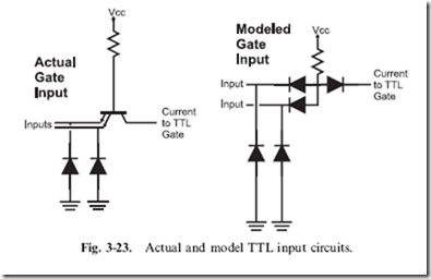
The standard TTL input consists of an NPN bipolar transistor wired in the unusual configuration shown in Fig. 3-23. On the left side of this diagram, I have drawn a two input TTL gate which is implemented with a two emitter
NPN transistor – as unusual as this type of transistor sounds, they really do exist. To understand how the input works, I replaced the two emitter NPN transistor with the three diode equivalent ‘‘model’’ on the right side of Fig. 3-23.
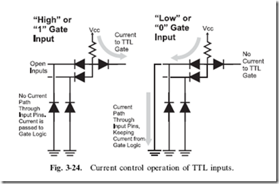
Normally, an NPN transistor passes current from its base to the emitter, but when wired in the TTL input configuration, the base current does not have a path through the transistor’s emitters and passes through the transistor’s collector to the gate logic. Figure 3.24 shows this situation along the other case where one of the input transistor’s emitter’s is tied to ground and the base current passes through the emitter and not the collector. The logic connected to the input NPN transistor’s collector responds depending on whether or not current is available from the collector.
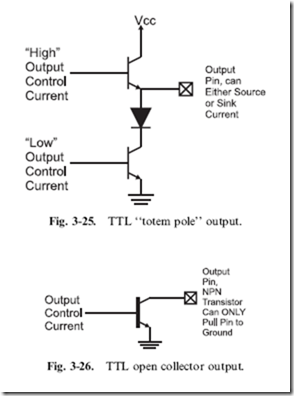
Obviously a simple switch, connected to ground, will allow current to pass through the emitter but you are probably wondering how other logic devices can control this device. A typical logic device output looks like Fig. 3-25 and consists of two transistors: one that will connect the output to the device power and one that will connect the output to the device ground. This transistor path to ground will provide the emitter current path of the chip.
When the output is a high voltage (the top transistor is on and the bottom one is off), no current will flow into the TTL input gate because of the reverse diode nature of the emitter input pin.
The TTL output shown in Fig. 3-25 is known as a ‘‘totem pole’’ output because of its resemblance to its namesake. If you were to connect a totem pole output to a TTL input and measured the voltage at the input or output pins, you would see a high voltage, which the gate connected to the input
would respond to as a ‘‘1’’. When a low voltage is output, the TTL gate will respond as if a ‘‘0’’ was input. What you are not measuring is the current flow between the two pins.
There are two terms used in Fig. 3-25 that I should explain. When a
transistor is connected to the power supply of a chip and is turned on, it is said to be ‘‘sourcing’’ current. When a transistor is connected to ground and is turned on, the transistor is said to be a current ‘‘sink’’. I will use these terms throughout the book and you will see in other books and references any time a device is either supplying (‘‘sourcing’’) or taking away (‘‘sinking’’) current.
There is another type of output which does not source any current and is
known as the open collector output (Fig. 3-26). This output typically has two uses. The first is it can pull down voltages which are greater than the positive voltage applied to the chip. Normally these voltages are less than 15 V and can only source 10 to 20 mA. For higher currents and voltages, discrete transistors must be used.
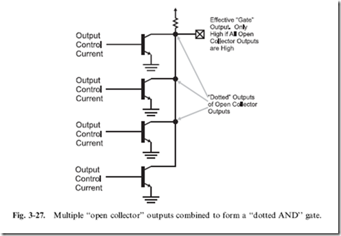
By not sourcing any current, these outputs can be ‘‘ganged’’ together in parallel, as I have shown in Fig. 3-27. This circuit is known as a ‘‘dotted AND’’ because it only outputs a 1 if all the outputs are ‘‘high’’ and each
transistor is ‘‘off ’’ and not pulling the common output line to ground. Note that there must be a pull up resistor connected to the output to provide a high-voltage, low-current source. Dotted AND gates are useful in a variety of different situations ranging from circuits where an arbitrary number of outputs can control one line or where digital outputs and buttons are combined. (I will discuss this in more detail later in the book.)
Totem pole outputs are the recommended default gate output because you can easily check voltage levels between intermediate gates in a logic string. As I will show later in this chapter, you cannot use a voltmeter or logic probe to check the logic levels if a TTL gate is driven by an open collector output.
Along with this, a CMOS input is connected to an open collector (or open drain, as I will discuss below) output. Then there will be no high voltage for the gate to operate. The only cases where an open collector/open drain output should be used is when you are wiring a dotted AND gate or are switching an input that is operating at a voltage different from the gate’s power.
TTL output pins are internally limited to only sink or source around 20 mA of current, which limits the number of inputs that it can drive. If you were to do the math, you would discover that when a TTL input is pulled low, 1.075 mA of current is passed through the output pin (this was found by assuming the base/emitter voltage of a transistor is 0.7 volts and the current limiting resistor connected to the input transistor’s base is 4 k, which is typical for TTL inputs.
Along with the totem pole and the open collector outputs, there is also the ‘‘tri-state driver’’ output, which cannot only source or sink current but can be turned ‘‘off ’’ to electrically isolate itself from the circuit that it is connected to. I will discuss tri-state drivers later in the book, when I present busses and multiple devices on the same line.
Knowing that each TTL input requires a current sink of just over 1 mA and most TTL outputs can sink up 20 mA, you might expect the maximum number of TTL inputs driven by a single output (which is called ‘‘fanout’’) to be 18 or 19. The actual maximum fanout is 8 to ensure that there is a comfortable margin in the output to be able to pull down each output in a timely manner. Practically, I would recommend that you try to keep the number of inputs driven by an output to two and never exceed four. Some different technologies that you work with, do not have the same electrical drive characteristics and may not be designed to pull down eight inputs of another technology; so, to be on the safe side, always be very conservative with the number of inputs you drive with a single output.
Re-reading the last sentence of the previous paragraph, you might wonder if any potential low-drive situations could be improved by wiring multiple outputs together. This must be avoided because of the danger that the gates will switch at different times, resulting in large currents passing through the gate output circuitry, and not through the net the outputs are connected to.
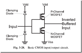
The CMOS logic gate input (Fig. 3-28) is quite a bit simpler than the TTL gate input and much easier to understand. The CMOS input and, as I will
explain, the output, consist of a balanced P-channel MOSFET and an N-channel MOSFET wired as a very high gain amplifier. The slightest positive or negative voltage applied to this input circuit will cause the
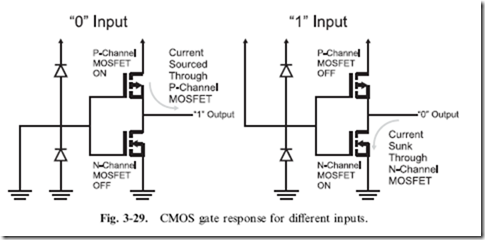
appropriate transistor to turn on and either source current (in the case where a negative voltage is applied and the P-channel MOSFET turns on) or sink current (a positive voltage will turn on the N-channel MOSFET). This operation can be seen in Fig. 3-29.
One interesting aspect of the two MOSFET transistors that I have shown wired as an inverter is that they not only provide the ability to sense and respond to voltage inputs, but as the voltage controls transistor switches, they are also effective totem pole output circuits as well. Not only are MOSFET transistors much easier to place on a piece of silicon semiconductor and can be placed in a smaller amount of surface area but also gates built from them are also much simpler than their TTL counterparts.
When the P-channel MOSFET is removed from the output of a CMOS gate, its output is said to be ‘‘open drain’’. This term refers to the drain of the N-channel MOSFET that is not connected to a transistor which can source current in just the same way as an ‘‘open collector’’ TTL output transistor and does not have a transistor which can source current. The CMOS logic open drain output works exactly the same way as the TTL open collector
output.
The two ‘‘clamping diodes’’ are placed in the circuit to hold the voltages to within Vdd (power input) and Vss (ground) and are primarily there to protect the P-channel and N-channel MOSFETs from damage from static electricity.
These diodes also provide you with the ability to power a CMOS chip through its input pins; when no voltage is applied to Vdd but there is a high-voltage input to one or more input pins, the clamping diodes will allow current to pass to the internal MOSFETs and power the circuit. This is usually an undesirable side effect and one that you should watch for.
The clamping diode function is provided in TTL by the diode and the bipolar transistor emitter that makes up a TTL gate input. Whereas CMOS logic requires additional diodes built into the circuitry, TTL has this function built in.
Unlike TTL, CMOS logic is voltage controlled; there is no path for current to enter or leave the MOSFET’s gate circuitry. This has some interesting side effects that you should be aware of. The first is that while at first glance of the inverter operation in Fig. 3-29 it appears that there is no current flow if the output of the CMOS input transistors was another CMOS gate, there actually is a very small amount of change passed to the gates of the transistor from Vdd when the P-channel MOSFET is turned on and this charge is sunk to Vss when the N-channel MOSFET is turned on. This transfer of charge grows with the number of CMOS gates as well as the speed that the gates switch; the faster they switch the more charge that is transferred over time.
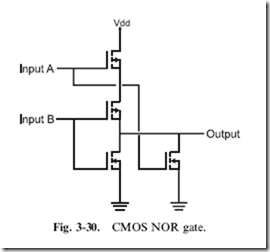
As I discussed at the start of this chapter, the measurement of charge movement over time is current. Earlier in the book, I said that the basic gate used in CMOS logic circuits is the NOR gate (just as the NAND gate is the basic gate used in TTL). Before leaving this chapter, I would like to show you the circuit used by a CMOS NOR gate (Fig. 3-30). If you trace through the operation of the four MOSFETs that make up this circuit, you will discover that the only time both P-channel MOSFETs are on (and voltage/current from Vdd is passed to the ‘‘Output’’) is when the two inputs are low, which matches the expected operation of the NOR gate.
The reason why the NOR gate was selected for use as the basic CMOS logic gate has to do with how MOSFETs and other circuits are put
down on a silicon semiconductor. The NOR gate is the most efficient while the NAND (which would make the basic building blocks of TTL and CMOS logic the same) cannot be accomplished as easily and in as small amount of space.
The last point I want to make about inputs and outputs is how to wire them when you want to hold them at a specific state (high/‘‘1’’ or low/‘‘0’’).
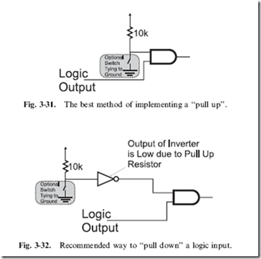
While you could connect the pins directly to power (for a high input) and ground (for a low input), I want to show you the recommended way of doing this and explain why you should go through the extra effort. Connecting the input to high value is accomplished using a 10 k resistor (called a ‘‘pull up’’), as I show in Fig. 3-31. This circuit will allow input to be temporarily wired to ground (for testing or circuit debug), without causing a short circuit (a low-resistance path between positive and negative power voltage).
Providing a ‘‘pull down’’ (connection to ground) is not quite so simple; the single resistor pull up of Fig. 3-31 is input into an inverter, as shown in Fig. 3-32. This circuit allows the pull up to be connected to ground for testing and debug (changing the input of the gate to a high from a solid low) just as in the pull up case.
If you have followed the gate explanations up to this point, you might be feeling like these methods of tying the gates to pull ups and pull downs is ‘‘overkill’’. I admit that these methods may seem more complex than just wiring the inputs to positive or negative power, but there are a number of reasons for specifying that pull ups and pull downs are wired in this way. For TTL, to make an input high all the time it can be simply left unconnected and to pull it down it can be pulled directly to ground; the 1 mA of current that will flow through the gate to ground should not be an excessive amount of current. For CMOS logic, the input pin can be tied directly to Vdd (positive power) for a high input and Vss (negative power) for a low input – there will be no current flow in either case. It is important to understand the three reasons why I recommend using the pull up resistor or the pull up resistor and inverter.
First, as I said above, it allows you to temporarily change the input value by connecting the resistor voltage to negative voltage without worrying about damaging any part of the circuit. Secondly, it allows simple test equipment to change the state of the input pin for testing without potentially overloading the circuit or the tester. This is a very important consideration when you are designing a product for mass production. Finally, this method can be used for both TTL and CMOS logic without regard to what type of logic is being used. I realize that going through the rigor of following these recommendations increases the complexity of a circuit as well as increasing the number of gates required, its cost and power consumption. In many cases, you will not feel that it is necessary, but if you decide to forgo using pull ups and inverted pull ups, make sure you understand what are the tradeoffs and the risks of the decision.
Simple Digital Logic Circuit Development
Many people do not realize that it is quite easy to build sample digital electronic logic circuits that demonstrate the concepts that have been presented to you as well as let you try out your own simple experiments. If you have, or are taking, a course in digital electronics, it probably includes a well-equipped laboratory in which you worked through a number of experiments. You do not need to replicate this laboratory at home if you wish to experiment with digital electronics. As I will show in this chapter, you can come up with a very capable digital logic circuit test kit for less than $20 and use parts available in modest electronics stores (like ‘‘Radio Shack’’).
Chances are, you are familiar with a variety of different electrical power sources: the ones that comes to mind first are batteries. There are a confusing number of different batteries that you can choose from, ranging from simple ‘‘AA’’ batteries that cost a few cents to the batteries used in the International Space Station that weigh (on Earth) 1200 pounds and cost over $200,000 each. Along with batteries, electricity can also be produced by generators, solar cells and fuel cells. Within your home you can access electrical power very conveniently through outlets in the walls, although this power is alternating current (‘‘AC’’) and not the direct current (‘‘DC’’) required for digital logic. AC power coming from the sockets in your home will have to be reduced and rectified into DC.
When you are experimenting with simple electronics, I think it’s best to use a power source that is definitely ‘‘low end’’; ‘‘alkaline’’ and rechargeable nickel–metal hydride (‘‘NiMH’’) batteries are widely available to power your experiments. TTL digital electronic chips generally operate between 4.5 and
5.5 volts – you could come up with a combination of batteries that will provide 5 volts to your circuit, or convert a 9 volt radio battery output to 5 volts using a ‘‘regulator’’. Rather than going through this effort and potential expense for TTL, I am going to recommend that you use CMOS digital logic chips that can be powered by 9 volts directly.
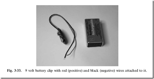
A 9 volt battery ‘‘clip’’ (Fig. 3-33) will cost you just a few cents and a bag of them can be bought for a dollar or so. For the purposes of the digital logic circuit test kit, you should look for a 9 volt battery clip that either has wire’s individual strands soldered together (the ends of the wires will look silver, shiny and attached together) or has a single strand. The wires will be covered
in a red and black plastic insulation and the strands will poke out the ends for a 1/4 inch or so.
Make sure the strands of the 9 volt battery clip wires are either soldered together or the wires consist of a single strand, because the wires from the battery clip will be pushed into holes and clamped by copper springs to provide power for the test circuits. Loose, individual strands break easily, can short with other loose wires or become a tangled mess, none of which are good things.
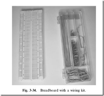
The battery clip is only one part of the wiring that will be used with the digital logic circuit test kit. By itself, the battery clip brings power out of the 9 volt battery conveniently, but is difficult to work with when you are working with chips and even moderately complex circuitry. The ‘‘breadboard’’ and wiring kit (Fig. 3-34) provide a customizable platform in which chips and other electronic components can be inserted into and easily wired together.
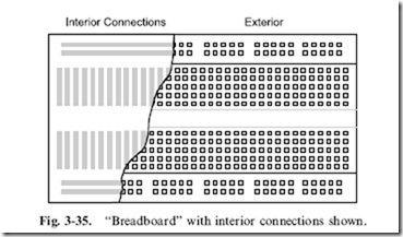
‘‘Breadboards’’ allow you to simply and quickly wire up your own prototyping circuits. From the top, a breadboard looks like a sea of holes, but if you were to ‘‘peel back’’ the top (Fig. 3-35), you would see that the holes are actually interconnected, with the central groups of holes connected outwards and the outermost two sets of holes connected along the length of the breadboard.
The central holes are spaced so that DIP chips can be placed in the breadboard and wired into the circuit easily. The outside two rows
of holes, I use as power ‘‘buss bars’’ and connect the power source to them directly.
Along with the breadboard, you can either buy a pre-cut and stripped wiring kit (shown in Fig. 3-34) or a roll of 24-gauge solid core wire and some needle nose pliers, wire clippers and maybe some wire strippers. For convenience, I usually go with the wiring kit as it costs just a few dollars.
Along with buying the battery clip, breadboard and wiring kit, you should also buy:
1. 5 or so LEDs in a 5 mm package
2. 10 or so 1k, 1/4 watt resistors
3. 10 or so 0.01 mF ceramic capacitors
4. One 555 oscillator/monostable chip
5. 5 or so SPDT switches, that can be inserted into the breadboard
6. One 74C00 quad two-input NAND gates chips
7. One 74C02 quad two-input NOR gates chips
8. One 74C04 hex inverter chip
9. One 74C08 quad two-input AND gates chip
10. One 74C32 quad two-input OR gates chip
11. One 74C74 dual D-flip flop chip.
All these parts should cost you less than $20 and are available at a fairly wide variety of sources including:
● Radio Shack (http://www.radioshack.com)
● Digi-Key (http://www.digikey.com)
● Mouser Electronics (http://www.mouser.com)
● Active Components (http://www.active-electronics.com).
You will not require any test equipment (such as a Digital Multi-Meter) for this kit and the sample circuits that I will present in this book.
Testing a Simple TTL Inverter
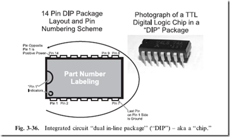
So far I have used the term ‘‘load’’ when I’ve described the electronic devices that are to be used in a circuit, but before going on, I want to familiarize you with the basic, ‘‘dual in-line package’’ ‘‘chip’’ (Fig. 3-36). The ‘‘chip’’ consists of a rectangular plastic box which has a series of metal pins (or connections) coming out from the two long sides. These pins are the electrical connections that are to be made to make up the digital logic circuits as well as provide power to the chip. As I have shown in Fig. 3-36, there can be one or two ‘‘pin 1’’ indicators on each chip (not all chips have both indicators) and the pins are numbered by going counterclockwise around the top of the chip. Before leaving this chapter, I would like to show both how easy it is to create a simple circuit to test out ideas and parts of applications as well as demonstrate how the TTL gate works. You should have a pretty good idea of how to wire in the chip, but you probably have some questions on how to create useful inputs and outputs to see what’s happening. The output will simply consist of a resistor and a LED – when the chip’s output is high, the LED will be on. Providing the same function for the input, a LED that is on
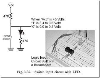
when the input is high is a bit more difficult and uses the circuit shown in Fig. 3-37.
This input circuit probably seems to be much more complex than I have led you to believe is necessary, but there are some requirements that were important for this circuit to meet so that it could be used in a variety of different situations. The first requirement was that it had to work for both TTL (using 5 volt power) as well as CMOS logic (powered from 5 to 9 volts). By providing a direct path to ground, the low voltage requirement of CMOS logic and the current path to ground for TTL was provided. Next, it had to light a LED when the input was high and turn it off when the input was low; the switch will provide a zero impedance current path for the current from the positive power to bypass the LED. Finally, it had to be easy for you to wire and check over in case it doesn’t seem to be working properly.
In Fig. 3-37, along with the logic input circuit schematic, I have included a photograph of the completed circuit built on a breadboard. In the photograph, notice that I have clipped the LED and resistor leads to keep the circuit as neat as possible on the breadboard. I strongly recommend that you keep components as close to the surface of the breadboard as possible to minimize your confusion when you are starting to build more complex
circuits.
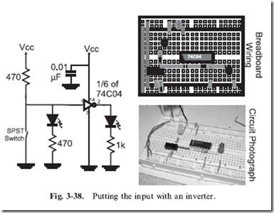
To demonstrate the operation of the inverter, you can build the circuit shown in the left side of Fig. 3-38 on your breadboard using the wiring diagram on the right side of Fig. 3-38. When the input LED is on, the output
LED will be off and vice versa. If one or the other LED does not light, then first check your wiring followed by the polarity of the LEDs – the flat side of
the LED must be connected to the negative voltage (Vss) connection of your circuit.
To build the inverter test circuit, you will need the following parts:
● Breadboard
● 9 volt battery
● 9 volt battery clip
● 74C04 CMOS hex inverter chip
● Two 5 mm LEDs
● Two 470 Q 1/4 watt resistors
● 1 k 1/4 watt resistor
● 0.01 mF capacitor (any type)
● Breadboard mountable switch (Digi-Key EG1903 suggested).
The only part that you might have some problems finding is the breadboard mountable switch (the EG1903 is a single-pole, double-throw switch with three posts 0.100 inch apart). This part is fairly unique and if you don’t want to go through the trouble of ordering the part from Digi-Key, you can either add wires to another switch or simply connect the circuit to the Vss connection to simulate the switch closing (in this case, the LED will go off indicating a low input, just as if a switch were in circuit).
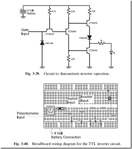
The 74Cxx family of chips are CMOS logic that are pin and output current compatible with 74LSxx TTL chips. The 74C04 used in the circuit shown in Fig. 3-38 demonstrates the operation of the NOT gate (or inverter) to quite good effect. The 74C04 does not demonstrate the operation of a TTL gate all
that well, so if you have a few moments, I suggest that you build the circuit shown in Fig. 3-39 (wired according to Fig. 3-40) and test it out – externally, it will seem to work identically to the 74C04 circuit shown in Fig. 3-38, but there are a few differences that you can experiment with.
The parts that you will need for this circuit are:
● Breadboard
● 9 volt battery
● 9 volt battery clip
● Four 2N3904 NPN bipolar transistors
● Two 1N914 (or equivalent) silicon diodes
● Two 5 mm LEDs
● 150 Q 1/4 watt resistor
● Two 470 Q 1/4 watt resistors
● 1 k 1/4 watt resistor
● 1.5 k 1/4 watt resistor
● 2.2 k 1/4 watt resistor
● 4.7 k 1/4 watt resistor
● 100 k 1/4 watt resistor
● 10 k potentiometer
● Breadboard mountable switch (Digi-Key EG1903 suggested).
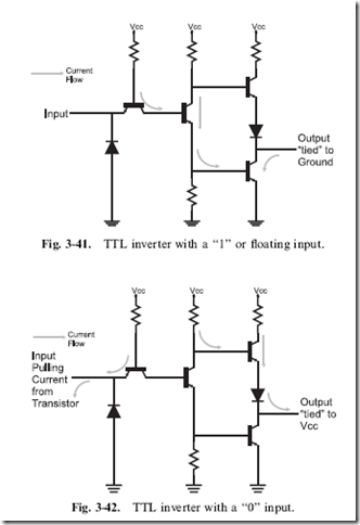
Going through the circuit, you can see that current flows through the circuit in two different directions, as shown in Figs. 3-41 and 3-42. When the input is
‘‘high’’ (LED on) and you follow the current path, you will see that the current will ultimately turn on the bottom right transistor, connecting the gate’s output pin to ground (‘‘low’’ voltage output). When current is drawn from the TTL input pin (Fig. 3-42), the current that ultimately turned on the bottom right transistor is taken away, resulting in a different path for currents within the gate. This change in current flow ultimately turns on the top right transistor, effectively tying the output to power and driving out a ‘‘high’’ voltage.
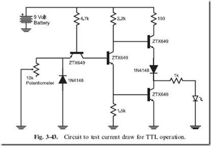
Once you have built the circuit and tested it, you can now look at the operating aspects of it by putting a potentiometer in the circuit, as I have shown in Fig. 3-43, and adjust it until the LED either flashes on and off or dims. If you have a digital multi-meter (DMM), you will find that the threshold current is about 1 mA, with a voltage across the potentiometer of
around 0.5 volts.
The final aspect of this experiment is to wire the inverter’s input as shown in Fig. 3-44 and alternatively connect the input (passing through the 100 k resistor) to the power in or ground. You will find that the LED never turns on regardless of the switch position. If you were to measure the voltage at the 100 k resistor, you would see that it is connected directly to the power and ground connections, but the circuit seems to ignore the ground connection.
The 100 k resistor prevents the 1 mA of current passing through to ground, resulting in the LED being turned on. If you were to repeat this experiment with the 74C04, you would see the LED turning on and off according to the voltage at the 100 k resistor.
In this chapter, I have given you a brief tutorial in basic electronics, an introduction to semiconductors and a method that you can use to build test circuits to experiment with digital electronics. In these few pages, I have covered the material included in several high school and college courses. It was not my intention to overwhelm you, but provide you with enough information to understand what is happening in a digital electronic circuit as well as give you a few basic rules to help you avoid problems, or if things aren’t working as you would expect, to have some ideas on where to look for the problems.
Quiz
1. Electricity must:
(a) Change polarity 60 times a second
(b) Flow between the planets
(c) Be equal in all parts of a circuit
(d) Flow in a closed, continuous loop
2. Every electrical circuit has three parts:
(a) Breadboards, batteries and electronic parts
(b) Power source, load and conductors
(c) Intelligence, compassion and a sense of humor
(d) Speed, power (or torque) and corporeal form
3. In the water pipe/tap/hose example, if you were to partially close the tap:
(a) Water would stream out faster from the hose
(b) The tap would get hot in your hand from the friction of the water passing through it
(c) The amount of water leaving the hose would decrease
(d) The water leaving the hose would stream further
4. In a single resistor circuit, if you apply 9 volts and measure 100 mA flowing through it, the resistance value is:
(a) 9 ohms
(b) 900 ohms
(c) 90 ohms
(d) 1,111 ohms
5. The equivalent resistance of a 10 ohm and 20 ohm resistor in parallel:
(a) Is always zero
(b) 30 ohms
(c) 7.5 ohms
(d) 6.7 ohms
6. A diode is said to be ‘‘forward biased’’ when:
(a) A positive voltage is applied to the ‘‘bar’’ painted on the side of the diode
(b) Electrons are injected into the P-type semiconductor of the diode
(c) Current flows into the diode through the end which doesn’t have a band painted on it
(d) More than 0.7 volts is applied to it
7. If a bipolar transistor with an hFE of 150 had a ‘‘small signal operating region’’ base current of 1 mA to 1 mA, what base current would be required to allow 10 mA collector current?
(a) This is impossible to answer because 10 mA collector current is greater than 1 mA.
(b) 1 mA
(c) 67 mA
(d) 667 mA
8. The basic TTL gate is:
(a) The NOT gate
(b) The AND gate
(c) The NOR gate
(d) The NAND gate
9. Totem pole outputs are best used:
(a) When there are multiple outputs tied together as a ‘‘dotted AND’’
(b) To drive electric motors
(c) As the default output type used in digital electronic circuits
(d) When high-speed operation of the digital electronic circuit is required
10. The dual in-line package:
(a) Is a standard method for packaging digital electronic chips
(b) Is used because part numbers cannot be stamped on bare chips
(c) Allows for an easy visual check to see whether or not the part was damaged by heat
(d) Facilitates effective cooling to the chip inside
