Example 11.8
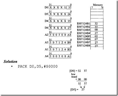
Determine the effect of execution of each of the following
PACK and UNPK instructions:
Assume the following data prior to execution of each of the above instructions:
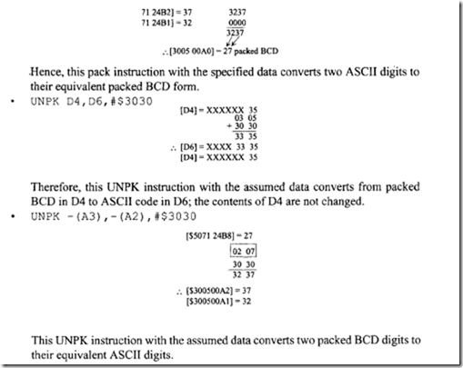
Note that ASCII code for 2 is $32 and for 7 is $37. Hence, this pack·instruction converts ASCII code to packed BCD.
PACK -(Al),-(A4),$0000
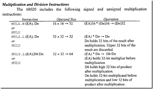 (EA) can use all modes except An. The condition codes N: Z. and V are affected; C is always cleared to 0, and X is unaffected for both MULS and MULU. For signed multiplication, overflow (V = I) can only occur for 32 x 32 multiplication, producing a 32-bit result if the high-order 32 bits of the 64-bit product are not the sign extension of the low-order 32 bits. In the case of unsigned multiplication, overflow (V = I) can occur for 32 x 32 multiplication, producing a 32-bit result if the high-order 32 bits of the 64-bit product are not zero.
Both MULS and MULU have a word form and a long word form. For the word form ( 16 x 16), the multiplier and multiplicand are both 16 bits and the result is 32 bits. The result is saved in the destination data register. For the long word form (32 x 32), the multiplier and multiplicand are both 32 bits and the result is either 32 bits or 64 bits. When the result is 32 bits for a 32-bit x 32-bit operation, the low-order 32 bits of the 64-bit product are provided.
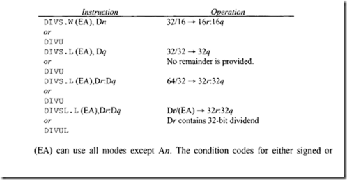
The signed and unsigned division instructions of the 68020 include the following, in which the source is the divisor, the destination is the dividend.
unsigned division are affected as follows: N = 1 if the quotient is negative; N = 0 otherwise. N is undefined for overflow or divide by zero. Z = 1 if the quotient is zero; Z = 0 otherwise. Z is undefined for overflow or divide by zero. V = 1 for division overflow; V = 0 otherwise. X is unaffected. Division by zero causes a trap. If overflow is detected before completion of the instruction, V is set to 1, but the operands are unaffected.
Both signed and unsigned division instructions have a word form and three long word forms. For the word form, the destination operand is 32 bits and the source operand is 16 bits. The 32-bit result in Dn contains the 16-bit quotient in the low word and the 16- bit remainder in the high word. The sign of the remainder is the same as the sign of the dividend.
For the instruction
 the destination is 64 bits contained in any two data registers and the source is 32 bits. The 32-bit register Dr (D0-D7) contains the 32-bit remainder and the 32-bit register Dq (D0-D7) contains the 32-bit quotient.
For the instruction
 the 32-bit register Dr (D0-D7) contains the 32-bit dividend and the source is also 32 bits. After division, Dr contains the 32-bit remainder and Dq contains the 32-bit quotient.
Example 11.9
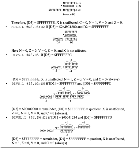
Determine the effect of execution of each of the following multiplication and division instructions:
-
MULU. L # $2, D5 if [D5] = $FFFFFFFF
-
MULS. L #$2,D5 if [D5] = $FFFFFFFF
-
MULU. L # $2,D5: D2 if [D5] = $2ABC 1800 and [D2] = $FFFFFFFF
-
DIVS.L #$2,D5 if[D5]=$FFFFFFFC
-
DIVS. L #$2, 02: D0 if [D2] = $FFFFFFFF and [D0]= $FFFFFFFC
-
DIVSL. L #$2, D6: D1 if [D1] = $00041234 and [D6] = $FFFFFFFD
Solution
-
MULU.L #$2,D5if[D5]=$FFFFFFFF
Therefore, [D5] = $FFFFFFFE, N = 0 since the most significant bit of the result is 0, Z = 0 because the result is nonzero, V = 1 because the high 32 bits of the 64-bit product are not zero, C = 0 (always), and X is not affected.
-
MULS.L #$2,D5 if[D5]=$FFFFFFFF
MC68HC000 Enhanced Instructions
The MC68020 includes the enhanced version of the instructions as listed next:
Note that Scan be B, W, or L. In addition to 8- and 16-bit signed displacements for BRA, Bee, and BSR like the 68HC000, the 68020 also allows signed 32-bit displacements. LINK is unsized in the 68HC000. (EA) in CMPI and TST supports all 68HC000 modes plus PC relative. An example is CMPI.W #$2000, (START, PC). In addition to EXT.W Dn and EXT.L Dn like the 68HC000, the 68020 also provides an EXTB.L instruction.
Example 11.10
Write a program in 68020 assembly language to multiply a 32-bit signed number in D2 by a 32-bit signed number in D3 by storing the multiplication result in the following manner:
(a) Store the 32-bit result in D2.
(b) Store the high 32 bits of the result in D3 and the low 32 bits of the result in D2.
Solution
Example 11.11
Write a program in 68020 assembly language to convert 10 packed BCD bytes (20 BCD digits) stored in memory starting at address $00002000 and above, to their ASCII equivalents and, store the result in memory locations starting at $FFFF8000.
Solution
M68020 Pins and Signals
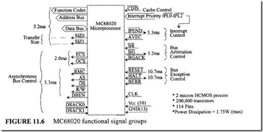
The 68020 is arranged in a 13 x 13 matrix array ( 114 pins defined) and fabricated in a pin grid array (PGA) or other packages such as RC suffix package. Both the 32-bit address (A0-A31) and data (D0-D31) pins of the 68020 are nonmultiplexed. The 68020 transfers data
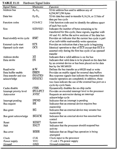
with an 8-bit device via D31-D24,with a 16-bit device via D16-D31,and with a 32-bit device via D31-D0• Figure 11.6 shows the MC68020 functional signal group. Table 11.11 lists these signals along with a description of each. There are 10 Vcc (+5 V) and 13 ground pins to distribute power in order to reduce noise.
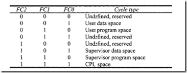
Like the MC68HC000, the three function code signals FC2, FC 1, and FCO identify the processor state (supervisor or user) and the address space of the bus cycle currently being executed except that the 68020 defines the CPU space cycle as follows:
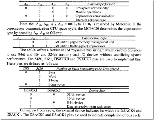
Note that in the 68HC000, FC2, FCl, FC0 = 111 indicates the interrupt acknowledge cycle. In the MC68020, it indicates the CPU space cycle. In this cycle, by decoding the address Jines A 19-A16, the MC68020 can perform various types of functions such as coprocessor communication, breakpoint acknowledge, interrupt acknowledge, and module operations as follows:
At the start of a bus cycle, the 68020 always transfers data to lines D0-D31, taking into consideration that the memory or I/O device may be 8, 16, or 32 bits wide. After the first bus cycle, the 68020 knows the device size by checking the DSACK0 and DSACKI pins and generates additional bus cycles if needed to complete the transfer.
Unlike the 68HC000, the 68020 permits word and long word operands to start at an odd address. However, if the starting address is odd, additional bus cycles are required to complete the transfer. For example, for a 16-bit device, the 68020 requires 2 bus cycles for a write to an even address such as MOVE . L D 1, $ 4 0 0 0 2 0 50 to complete the operation. On the other hand, the 68020 requires 3 bus cycles for MOVE . L D 1, $4 0 0 0 2 0 51 for a 16-bit device to complete the transfer. Note that, as in the 68HC000, instructions in the 68020 must start at even addresses.
Next, consider an example of dynamic bus sizing. The four bytes of a 32-bit data can be defined as follows:
If this data is held in a data register Dn and is to be written to a memory or I/O location, then the address lines A 1 and A0 define the byte position of data. For a 32-bit device, A 1A0 = 00 (addresses 0, 4, 8, ……), A 1A0 = 01 (addresses 1, 5, 9, …), A 1A0 = 10 (addresses 2, 6, 10, …),and A 1A0 =II (addresses 3, 7, II, …) will store OPO, OPI, OP2, and OP3, respectively. This data is written via the 68020 D31-D0 pins. However, if the device is 16-bit, data is always transferred as follows:
All even-addressed bytes via pins D31-D24 .
All odd-addressed bytes via pins D23-D16.
Finally, for an 8-bit device, both even- and odd-addressed bytes are transferred via pins D31-D24·
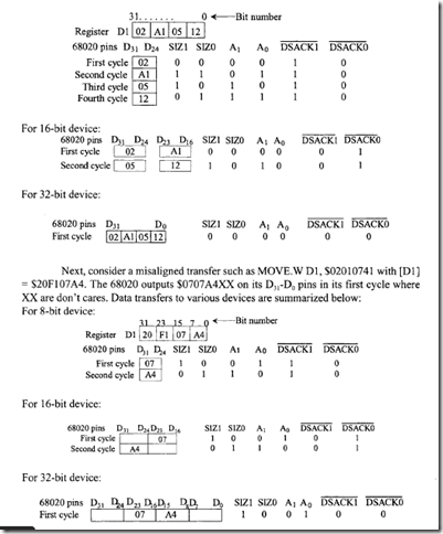
The 68020 always starts transferring data with the most significant byte first. As an example, consider MOVE . L D 1, $ 2 0 10 7 4 2 0. In the first bus cycle, the 68020 does not know the size of the device and, hence, outputs all combinations of data on pins D31-D0, taking into consideration that the device may be 8, 16, or 32 bits wide. Assume that the content of Dl is $02Al0512 (OPO = $02, OPI =$AI, OP2 = $05, and OP3 = $12). In the first bus cycle, the 68020 sends SIZl SIZO = 00, indicating a 32-bit transfer, and then outputs data on its D31-D0 pins as follows:
If the device is 8-bit, it will take data $02 from pins D31-D24 in the first cycle and will then assert DSACKI and DSACKO as 10, indicating an 8-bit device. The 68020 then transfers the remaining 24 bits ($A 1 first, $05 next, and $12 last) via pins D31-D24 in three consecutive cycles, with a total of four cycles being necessary to complete the transfer.
However, if the device is 16-bit, in the first cycle the device will take the 16-bit data $02Al via pins D31-D16 and will then assert DSACKI and DSACKO as 01, indicating a 16-bit device. The 68020 then transfers the remaining 16 bits ($0512) via pins D31-D16 in the next cycle, requiring a total of two cycles for the transfer.
Finally, if the device is 32-bit, the device receives all 32-bit data $02A 10512 via pins D31-D0 and asserts DSACKI DSACKO = 00 to indicate completion of the transfer. Aligned data transfers for various devices are as follows :
For 8-bit device:
Let us explain some of the other 68020 pins.
The ECS (external cycle start) pin is an MC68020 output pin. The MC68020 asserts this pin during the first one half clock of every bus cycle to provide the earliest indication of the start of a bus cycle. The use of ECS must be validated later with AS, because the MC68020 may start an instruction fetch cycle and then abort it if the instruction is found in the cache. In the case of a cache hit, the MC68020 does not assert AS, but provides A31-A0, SIZl, SIZO, and FC2-FCO outputs.
The MC68020 AVEC input is activated by an external device to service an autovector interrupt. The AVEC has the same function as VPA on the 68HC000. The functions of the other signals, such as AS, RJW, IPL2- IPLO, BR, BG, and BGACK, are similar to those of the MC68HC000.
The MC68020 system control pins are functionally similar to those of the MC68HC000. However, there are some minor differences. For example, for hardware reset, RESET and HALT pins need not be asserted simultaneously. Therefore, unlike the 68HC000, the RESET and HALT pins are not required to be tied together in the MC68020 system.
The RESET and HALT pins are bidirectional and open drain (external pull-up resistances are required), and their functions are independent. The RESET signal is a bidirectional signal. The RESET pin, when asserted by an external circuit for a minimum of 520 clock periods, the RESET pin resets the entire system including the MC68020. Upon hardware reset, the MC68020 completes any active bus cycle in an orderly manner and then performs the following:
-
Reads the 32-bit content of address $00000000 and loads it into the ISP (the contents of $00000000 are loaded to the most significant byte of the ISP and so on).
-
Reads the 32-bit contents of address $00000004 into the PC (contents of $00000004 to most significant byte of the PC and so on).
-
Sets the 12 11 10 bits of the SR to 1 1 1, sets the S bit in the SR to 1, and clears the T1 , T0, and M bits in the SR.
-
Clears the VBR to $00000000.
-
Clears the cache enable bit in the CACR.
-
All other registers are unaffected by hardware reset.
When the RESET instruction is executed, the MC68020 asserts the RESET pin for 512 clock cycles and the processor resets all the external devices connected to the RESET pin. Software reset does not affect any internal register.
As mentioned earlier while describing dynamic bus sizing, the 68020 always drives all data lines during a write operation. Furthermore, for all inputs there is a sample window of at least 20 ns during which the 68020 latches the input level. To guarantee the recognition of a certain level on a particular falling edge of the clock, the input level must be held stable throughout this sample window, 20 ns; otherwise, the level recognized by the MC68020 is unknown or legal.
During data transfer operations, the 68020 can use either synchronous or asynchronous operation. In synchronous operation, the 68020 clock is used to generate DSACK1, DSACK0, and other asynchronous inputs. Also, in synchronous operation, if the DSACKl and DSACK0 are asserted for the required window of at least 20 ns (at least 5 ns before and at leastl5 ns after the falling edge of S2) on the falling edge S2, the 68020 latches valid data on the falling edge of S4 on a read cycle. The 68020 does not generate any wait states if DSACK1 and DSACK0 are asserted at the falling edge ofS2; otherwise the 68020 inserts wait cycles like the 68HC000 and latches data at the falling edge of the following cycle as soon as DSACK1 and DSACK0 are asserted. A minimum of three clock cycles are required for a read operation.
In asynchronous operation, clock frequency independence at a system level is achieved and the 68020 is used in an asynchronous manner. This typically requires using the bus signals such as AS, DS, DSACKI, and DSACKO to control data transfer. Using asynchronous operation, AS starts the bus cycle and DS is used as a condition of valid data on a write cycle. Decoding of SIZ 1, SIZO, A 1, and A0 provides enable signals, which indicate the portion of the data bus that is used in data transfer. The memory or I/O chip then responds by placing the requested data on the correct portion of the data bus for a read cycle or latching the data on a write cycle and asserting DSACK1, and DSACKO, corresponding to the memory or I/O port size (8-bit, 16-bit, or 32-bit), to terminate the bus cycle. If no memory or I/O device responds or the address is invalid, the external control logic asserts the BERR or BERR and HALT signal(s) to abort or retry the bus cycle or retries the bus cycle.
In asynchronous operation, the DSACKI, and DSACKO signals are allowed to be asserted before the data from memory or an I/O device is valid on a read cycle. The 68020 latches data according to Parameter #31 provided in Motorola manuals. (Parameter #31 is a maximum of 60 ns for the 12.5-MHz 68020, a maximum of 50 ns for the 16.67-MHz 68020, and a maximum of 43 ns for the 20-Mhz 68020, and maximum time is specified from the assertion of AS to the assertion ofDSACK1, and DSACKO. This is because the 68020 will insert wait cycles in one-clock-cycle increments until DSACKI, and DSACKO are recognized as asserted.)

