Input/Output Allocation
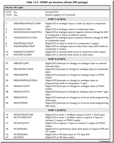
The I/O functions provided by the PIC 16F887 are detailed in Table 13.2. These were mapped against the requirements of the application, and the most convenient grouping was decided, giving the I/O allocation in Table 13.3.
Circuit Description
Figure 13.3 shows the schematic for the temperature controller. Each interface will be described separately. The default internal 4 MHz clock is used, to give a convenient instruction execution time, although no timing critical operations are required in this application.
Analogue Inputs
The four temperature sensors are connected to port A, with four pots providing dummy inputs. It is expected that standard calibrated sensors (LM35 or similar) with an output of 10 mV/oC will be used (0oC ¼ 0 mV). The controller is designed to operate at up to 50oC, at which temperature the sensor output is 500 mV. This low voltage is acceptable if the sensors are not connected on long leads, which could pick up electrical interference. For more remote operation, a dc amplifier should be used at the sensor end of the connection to increase the voltage to, say, 5.00 V at 50oC, and the analogue-to-digital converter (ADC) rescaled accordingly. Screened leads should also be used. The inputs are protected from noise and
overvoltage by a 1k/1nF low pass filter; the input impedance at the ADC is high enough for this to have a negligible effect on the input voltage measurement.
The ADC normally operates at 10-bit resolution, giving output values in the range 0e1023. It needs reference voltages to set the maximum and minimum values for the input conversion.
These can be provided internally as VDD and VSS (supply values), but VDD does not give a convenient conversion factor. Therefore, an external reference value was provided from a
2.7 V Zener diode and potential divider, giving Vrefþ adjusted to 2.048 V. This gives a conversion factor of 2048/1024 ¼ 2 mV per bit. To simplify the software, and to cover the correct range, only the low 8 bits of the ADC result will be used in the test program, with a maximum value of 255. At 50oC, the input will be 500 mV/2 mV ¼ 250, giving a resolution of 0.2oC per bit. The test pots allow the input to set manually, to check the operation of the software without having to heat and cool the target system. These can be switched in and out as required via a bank of dual in-line package (DIP) switches.
Outputs
Two types of output device are provided: relay and FET. The relay allows the load circuit to be isolated (electrically separate) from the controller. The external circuit operates with its own supply, so the load (heater in this case) can be powered from a single or three-phase supply. The relay is easy to use, but its changeover is relatively slow, and the contacts may wear out in time. The FET interface is more reliable, as it is solid state. The disadvantage in this design is that the load has to operate from the same supply as the FET, the 5 V board supply. It also does not provide full electrical isolation between the controller and the load. However, the FET interface can be switched at high frequency, allowing PWM speed control, and could be modified for isolated operation. All the outputs include an on-board status light-emitting diode (LED).
Keypad
The 12-button keypad allows the user to input the required temperature and other operating parameters as required by the application program. The target temperature, upper and lower limits, alarm levels and so on would be input as two digits. The keypad is simply a set of switches connected in a row and column arrangement, and accessed by a scanning routine. If the row inputs (A, B, C, D) are all set high initially, and no button is pressed, all the column outputs (1, 2, 3) will be high (pulled up to 5 V). A ‘0’ is then output on each row in turn, and, if a button is pressed, that ‘0’ will appear at the column output and can be detected by the MCU. The combination of the active row and column identifies the key.
Display
A seven-segment display is used, as it is relatively easy to drive compared with the liquid crystal display (LCD), and is self-illuminating. The encoding has been covered in Chapter 10; a look-up table (Table 10.2) provides the output combination for each displayed digit. In this case, two digits are required, but they can both be operated from the same set of outputs by multiplexing. The digits are switched on alternately via Q1 and Q2, at a rate that is fast enough for the digits to appear to be on at the same time, albeit at reduced brightness. Since this effectively halves the average current, the current limiting resistors otherwise needed in the display outputs are unnecessary. Since the switching transistor is acting as a constant current source, and this current will be shared among those segments that are lit, there may be some variation in brightness depending on the digit displayed. This could be improved by using a constant voltage source to control the common terminal current.
Other Interfaces
A buzzer is fitted to provide an audible alarm output. This can be used to signal system failure or, for example, the temperature being too low for too long. Audible feedback from keystrokes is also desirable. A manual reset is provided, so that the program can be restarted without powering down. This will be useful for testing as well as in normal operation. In-circuit programming and debugging are provided via the ICPD connector. An ICD module must be connected between the host PC and the application board.


