THE 80386 AND 80486 MICROPROCESSORS
INTRODUCTION
The 80386 microprocessor is a full 32-bit version of the earlier 8086/80286 16-bit microprocessors, and represents a major advancement in the architecture—a switch from a 16-bit architecture to a 32-bit architecture. Along with this larger word size are many improvements and additional features. The 80386 microprocessor features multitasking, memory management, virtual memory (with or without paging), software protection, and a large memory system. All soft- ware written for the early 8086/8088 and the 80286 are upward-compatible to the 80386 micro- processor. The amount of memory addressable by the 80386 is increased from the 1M byte found in the 8086/8088 and the 16M bytes found in the 80286, to 4G bytes in the 80386. The 80386 can switch between protected mode and real mode without resetting the microprocessor. Switching from protected mode to real mode was a problem on the 80286 microprocessor because it required a hardware reset.
The 80486 microprocessor is an enhanced version of the 80386 microprocessor that exe- cutes many of its instructions in one clocking period. The 80486 microprocessor also contains an 8K-byte cache memory and an improved 80387 numeric coprocessor. (Note that the 80486DX4 contains a 16K-byte cache.) When the 80486 is operated at the same clock frequency as an 80386, it performs with about a 50% speed improvement. In Chapter 18, the Pentium and Pentium Pro are detailed. These microprocessors both contain a 16K cache memory, and perform at better than twice the speed of the 80486 microprocessor. The Pentium and Pentium Pro also contain improved numeric coprocessors that operate five times faster than the 80486 numeric coprocessor. Chapter 19 deals with additional improvements in the Pentium II–Core2 microprocessors.
Upon completion of this chapter, you will be able to:
1. Contrast the 80386 and 80486 microprocessors with earlier Intel microprocessors.
2. Describe the operation of the 80386 and 80486 memory-management unit and paging unit.
3. Switch between protected mode and real mode.
4. Define the operation of additional 80386/80486 instructions and addressing modes.
5. Explain the operation of a cache memory system.
6. Detail the interrupt structure and direct memory access structure of the 80386/80486.
7. Contrast the 80486 with the 80386 microprocessor.
8. Explain the operation of the 80486 cache memory.
INTRODUCTION TO THE 80386 MICROPROCESSOR
Before the 80386 or any other microprocessor can be used in a system, the function of each pin must be understood. This section of the chapter details the operation of each pin, along with the external memory system and I/O structures of the 80386.
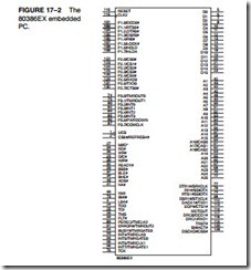
Figure 17–1 illustrates the pin-out of the 80386DX microprocessor. The 80386DX is pack- aged in a 132-pin PGA (pin grid array). Two versions of the 80386 are commonly available: the 80386DX, which is illustrated and described in this chapter and the 80386SX, which is a reduced bus version of the 80386. A new version of the 80386—the 80386EX—incorporates the AT bus system, dynamic RAM controller, programmable chip selection logic, 26 address pins, 16 data pins, and 24 I/O pins. Figure 17–2 illustrates the 80386EX embedded PC.
The 80386DX addresses 4G bytes of memory through its 32-bit data bus and 32-bit address. The 80386SX, more like the 80286, addresses 16M bytes of memory with its 24-bit address bus via its 16-bit data bus. The 80386SX was developed after the 80386DX for applications that didn’t require the full 32-bit bus version. The 80386SX was found in many early personal computers that used the same basic motherboard design as the 80286. At the time that the 80386SX was popular, most applications, including Windows 3.11, required fewer than 16M bytes of memory, so the 80386SX is a popular and a less costly version of the 80386 micro- processor. Even though the 80486 has become a less expensive upgrade path for newer systems, the 80386 still can be used for many applications. For example, the 80386EX does not appear in computer systems, but it is becoming very popular in embedded applications.
As with earlier versions of the Intel family of microprocessors, the 80386 requires a single
+5.0 V power supply for operation. The power supply current averages 550 mA for the 25 MHz version of the 80386, 500 mA for the 20 MHz version, and 450 mA for the 16 MHz version. Also available is a 33 MHz version that requires 600 mA of power supply current. The power supply current for the 80386EX is 320 mA when operated at 33 MHz. Note that during some modes of normal operation, power supply current can surge to over 1.0 A. This means that the power sup- ply and power distribution network must be capable of supplying these current surges. This device contains multiple VCC and VSS connections that must all be connected to +5.0 V and grounded for proper operation. Some of the pins are labeled N/C (no connection) and must not be connected. Additional versions of the 80386SX and 80386EX are available with a +3.3 V power supply. They are often found in portable notebook or laptop computers and are usually packaged in a surface mount device.
Each 80386 output pin is capable of providing 4.0 mA (address and data connections) or
5.0 mA (other connections). This represents an increase in drive current compared to the 2.0 mA available on earlier 8086, 8088, and 80286 output pins. The output current available on most 80386EX output pins is 8.0 mA. Each input pin represents a small load, requiring only ±10 μA of current. In some systems, except the smallest, these current levels require bus buffers.
The function of each 80386DX group of pins follows:
A31–A2 Address bus connections address any of the 1G × 32 (4G bytes) memory locations found in the 80386 memory system. Note that A0 and A1 are encoded in the bus enable (BE3 – BE0) to select any or all of the four bytes in a
![]() 32-bit-wide memory location. Also note that because the 80386SX contains a 16-bit data bus in place of the 32-bit data bus found on the 80386DX, A1 is pre- sent on the 80386SX, and the bank selection signals are replaced with BHE and BLE. The BHE signal enables the upper data bus half; the BLE signal enables the lower data bus half.
32-bit-wide memory location. Also note that because the 80386SX contains a 16-bit data bus in place of the 32-bit data bus found on the 80386DX, A1 is pre- sent on the 80386SX, and the bank selection signals are replaced with BHE and BLE. The BHE signal enables the upper data bus half; the BLE signal enables the lower data bus half.
![]()
![]() D31–D0 Data bus connections transfer data between the microprocessor and its memory and I/O system. Note that the 80386SX contains D15–D0.
D31–D0 Data bus connections transfer data between the microprocessor and its memory and I/O system. Note that the 80386SX contains D15–D0.
BE3 – BE0

 W>R ADS
Bank enable signals select the access of a byte, word, or doubleword of data. These signals are generated internally by the microprocessor from address bits A1 and A0. On the 80386SX, these pins are replaced by BHE, BLE, and A1. Memory/IO selects a memory device when a logic 1 or an I/O device when a logic 0. During the I/O operation, the address bus contains a 16-bit I/O address on address connections A15–A2.
![]()
![]()
![]() Write>Read indicates that the current bus cycle is a write when a logic 1 or a read when a logic 0.
Write>Read indicates that the current bus cycle is a write when a logic 1 or a read when a logic 0.
![]() The address data strobe becomes active whenever the 80386 has issued a valid memory or I/O address. This signal is combined with the W>R signal to gener- ate the separate read and write signals present in the earlier 8086–80286 micro- processor-based systems.
The address data strobe becomes active whenever the 80386 has issued a valid memory or I/O address. This signal is combined with the W>R signal to gener- ate the separate read and write signals present in the earlier 8086–80286 micro- processor-based systems.
RESET Reset initializes the 80386, causing it to begin executing software at memory location FFFFFFF0H. The 80386 is reset to the real mode, and the leftmost 12 address connections remain logic 1s (FFFH) until a far jump or far call is exe- cuted. This allows compatibility with earlier microprocessors.
![]() CLK2 Clock times 2 is driven by a clock signal that is twice the operating frequency of the 80386. For example, to operate the 80386 at 16 MHz, apply a 32 MHz clock to this pin.
CLK2 Clock times 2 is driven by a clock signal that is twice the operating frequency of the 80386. For example, to operate the 80386 at 16 MHz, apply a 32 MHz clock to this pin.

 READY LOCK D>C
Ready controls the number of wait states inserted into the timing to lengthen memory accesses.
Lock becomes a logic 0 whenever an instruction is prefixed with the LOCK: prefix. This is used most often during DMA accesses.
Data/control indicates that the data bus contains data for or from memory or I/O when a logic 1. If D>C is a logic 0, the microprocessor is halted or executes an interrupt acknowledge.
![]()
![]()
![]() Bus size 16 selects either a 32-bit data bus (BS16 = 1) or a 16-bit data bus (BS16 = 0). In most cases, if an 80386DX is operated on a 16-bit data bus, we use the 80386SX that has a 16-bit data bus. On the 80386EX, the BS8 pin selects an 8-bit data bus.
Bus size 16 selects either a 32-bit data bus (BS16 = 1) or a 16-bit data bus (BS16 = 0). In most cases, if an 80386DX is operated on a 16-bit data bus, we use the 80386SX that has a 16-bit data bus. On the 80386EX, the BS8 pin selects an 8-bit data bus.
Next address causes the 80386 to output the address of the next instruction or data in the current bus cycle. This pin is often used for pipelining the address.
HOLD Hold requests a DMA action.
![]() HLDA Hold acknowledge indicates that the 80386 is currently in a hold condition.
HLDA Hold acknowledge indicates that the 80386 is currently in a hold condition.
 PEREQ BUSY
The coprocessor request asks the 80386 to relinquish control and is a direct connection to the 80387 arithmetic coprocessor.
Busy is an input used by the WAIT or FWAIT instruction that waits for the coprocessor to become not busy. This is also a direct connection to the 80387 from the 80386.
 ERROR
ERROR
Error indicates to the microprocessor that an error is detected by the coprocessor.
INTR An interrupt request is used by external circuitry to request an interrupt.
NMI A non-maskable interrupt requests a non-maskable interrupt as it did on the earlier versions of the microprocessor.
The Memory System
The physical memory system of the 80386DX is 4G bytes in size and is addressed as such. If vir- tual addressing is used, 64T bytes are mapped into the 4G bytes of physical space by the mem- ory management unit and descriptors. (Note that virtual addressing allows a program to be larger than 4G bytes if a method of swapping with a large hard disk drive exists.) Figure 17–3 shows the organization of the 80386DX physical memory system.
The memory is divided into four 8-bit wide memory banks, each containing up to 1G bytes of memory. This 32-bit-wide memory organization allows bytes, words, or doublewords of memory data to be accessed directly. The 80386DX transfers up to a 32-bit-wide number in a single memory cycle, whereas the early 8088 requires four cycles to accomplish the same trans- fer, and the 80286 and 80386SX require two cycles. Today, the data width is important, espe- cially with single-precision floating-point numbers that are 32 bits wide. High-level software normally uses floating-point numbers for data storage, so 32-bit memory locations speed the execution of high-level software when it is written to take advantage of this wider memory.
Each memory byte is numbered in hexadecimal as they were in prior versions of the fam- ily. The difference is that the 80386DX uses a 32-bit-wide memory address, with memory bytes numbered from location 00000000H to FFFFFFFFH.
![]() The two memory banks in the 8086, 80286, and 80386SX system are accessed via BLE (A0 on the 8086 and 80286) and BHE. In the 80386DX, the memory banks are accessed via four bank
The two memory banks in the 8086, 80286, and 80386SX system are accessed via BLE (A0 on the 8086 and 80286) and BHE. In the 80386DX, the memory banks are accessed via four bank
![]()
![]() enable signals, BE3 – BE0. This arrangement allows a single byte to be accessed when one bank enable signal is activated by the microprocessor. It also allows a word to be addressed when two
enable signals, BE3 – BE0. This arrangement allows a single byte to be accessed when one bank enable signal is activated by the microprocessor. It also allows a word to be addressed when two
bank enable signals are activated. In most cases, a word is addressed in banks 0 and 1, or in banks 2 and 3. Memory location 00000000H is in bank 0, location 00000001H is in bank 1, location 00000002H is in bank 2, and location 00000003H is in bank 3. The 80386DX does not contain address connections A0 and A1 because these have been encoded as the bank enable signals. Likewise, the 80386SX does not contain the A0 address pin because it is encoded in the BLE and BHE signals. The 80386EX addresses data either in two banks for a 16-bit-wide memory system if BS8 = 1 or as an 8-bit system if BS8 = 0.
Buffered System. Figure 17–4 shows the 80386DX connected to buffers that increase fan-out from its address, data, and control connections. This microprocessor is operated at 25 MHz using a 50 MHz clock input signal that is generated by an integrated oscillator module. Oscillator modules are usually used to provide a clock in modern microprocessor-based equipment. The HLDA signal is used to enable all buffers in a system that uses direct memory access. Otherwise, the buffer enable pins are connected to ground in a non-DMA system.
Pipelines and Caches. The cache memory is a buffer that allows the 80386 to function more efficiently with lower DRAM speeds. A pipeline is a special way of handling memory accesses so the memory has additional time to access data. A 16 MHz 80386 allows memory devices with access times of 50 ns or less to operate at full speed. Obviously, there are few DRAMs currently available with these access times. In fact, the fastest DRAMs currently in use have an access time of 40 ns or longer. This means that some technique must be found to interface these memory devices, which are slower than required by the microprocessor. Three techniques are available: interleaved memory, caching, and a pipeline.
The pipeline is the preferred means of interfacing memory because the 80386 micro- processor supports pipelined memory accesses. Pipelining allows memory an extra clocking period to access data. The extra clock extends the access time from 50 ns to 81 ns on an 80386 operating with a 16 MHz clock. The pipe, as it is often called, is set up by the microprocessor. When an instruction is fetched from memory, the microprocessor often has extra time before the next instruction is fetched. During this extra time, the address of the next instruction is sent out from the address bus ahead of time. This extra time (one clock period) is used to allow additional access time to slower memory components.
Not all memory references can take advantage of the pipe, which means that some memory cycles are not pipelined. These nonpipelined memory cycles request one wait state if the normal pipeline cycle requires no wait states. Overall, a pipe is a cost-saving feature that reduces the access time required by the memory system in low-speed systems.
Not all systems can take advantage of the pipe. Those systems typically operate at 20, 25, or 33 MHz. In these higher-speed systems, another technique must be used to increase the memory system speed. The cache memory system improves overall performance of the mem- ory systems for data that are accessed more than once. Note that the 80486 contains an internal cache called a level 1 cache and the 80386 can only contain an external cache called a level 2 cache.
A cache is a high-speed memory (SRAM) system that is placed between the microproces- sor and the DRAM memory system. Cache memory devices are usually static RAM memory components with access times of less than 10 ns. In many cases, we see level 2 cache memory systems with sizes between 32K and 1M byte. The size of the cache memory is determined more by the application than by the microprocessor. If a program is small and refers to little memory data, a small cache is beneficial. If a program is large and references large blocks of memory, the largest cache size possible is recommended. In many cases, a 64K-byte cache improves speed sufficiently, but the maximum benefit is often derived from a 256K-byte cache. It has been found that increasing the cache size much beyond 256K provides little benefit to the operating speed of the system that contains an 80386 microprocessor.
Interleaved Memory Systems. An interleaved memory system is another method of improving the speed of a system. Its only disadvantage is that it costs considerably more memory because of its structure. Interleaved memory systems are present in some systems, so memory access times can be lengthened without the need for wait states. In some systems, an interleaved memory may still require wait states, but may reduce their number. An interleaved memory system requires two or more complete sets of address buses and a controller that provides addresses for each bus. Systems that employ two complete buses are called a two-way interleave; systems that use four complete buses are called a four-way interleave.
An interleaved memory is divided into two or four parts. For example, if an interleaved memory system is developed for the 80386SX microprocessor, one section contains the 16-bit addresses 000000H–000001H, 000004H–000005H, and so on; the other section contains addresses 000002–000003, 000006H–000007H, and so forth. While the microprocessor accesses locations 000000H–000001H, the interleave control logic generates the address strobe signal for locations 000002H–000003H. This selects and accesses the word at location 000002H–000003H, while the microprocessor processes the word at location 000000H–000001H. This process alternates memory sections, thus increasing the performance of the memory system.
Interleaving increases the amount of access time provided to the memory because the address is generated to select the memory before the microprocessor accesses it. This is because the microprocessor pipelines memory addresses, sending the next address out before the data are read from the last address.
The problem with interleaving, although not major, is that the memory addresses must be accessed so that each section is alternately addressed. This does not always happen as a program executes. Under normal program execution, the microprocessor alternately addresses memory approximately 93% of the time. For the remaining 7%, the microprocessor addresses data in the same memory section, which means that in these 7% of the memory accesses, the memory sys- tem must cause wait states because of the reduced access time. The access time is reduced because the memory must wait until the previous data are transferred before it can obtain its address. This leaves the memory with less access time; therefore, a wait state is required for accesses in the same memory bank.
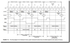
See Figure 17–5 for the timing diagram of the address as it appears at the microprocessor address pins. This timing diagram shows how the next address is output before the current data are accessed. It also shows how access time is increased by using interleaved memory addresses for each section of memory compared to a non-interleaved access, which requires a wait state.
![]() Figure 17–6 pictures the interleave controller. Admittedly, this is a complex logic circuit, which needs some explanation. First, if the SEL input (used to select this section of the memory) is inactive (logic 0), then the WAIT signal is a logic 1. Also, both ALE0 and ALE1, used to strobe the address to the memory sections, are both logic 1s, causing the latches connected to them to become transparent.
Figure 17–6 pictures the interleave controller. Admittedly, this is a complex logic circuit, which needs some explanation. First, if the SEL input (used to select this section of the memory) is inactive (logic 0), then the WAIT signal is a logic 1. Also, both ALE0 and ALE1, used to strobe the address to the memory sections, are both logic 1s, causing the latches connected to them to become transparent.
![]() As soon as the SEL input becomes a logic 1, this circuit begins to function. The A1 input is used to determine which latch (U2B or U5A) becomes a logic 0, selecting a section of the mem- ory. Also the ALE pin that becomes a logic 0 is compared with the previous state of the ALE pins. If the same section of memory is accessed a second time, the WAIT signal becomes a logic 0, requesting a wait state.
As soon as the SEL input becomes a logic 1, this circuit begins to function. The A1 input is used to determine which latch (U2B or U5A) becomes a logic 0, selecting a section of the mem- ory. Also the ALE pin that becomes a logic 0 is compared with the previous state of the ALE pins. If the same section of memory is accessed a second time, the WAIT signal becomes a logic 0, requesting a wait state.
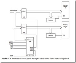
Figure 17–7 illustrates an interleaved memory system that uses the circuit of Figure 17–6. Notice how the ALE0 and ALE1 signals are used to capture the address for either section of memory. The memory in each bank is 16 bits wide. If accesses to memory require 8-bit data, the system causes wait states, in most cases. As a program executes, the 80386SX fetches instructions 16 bits at a time from normally sequential memory locations. Program execution uses inter- leaving in most cases. If a system is going to access mostly 8-bit data, it is doubtful that memory interleaving will reduce the number of wait states.
The access time allowed by an interleaved system, such as the one shown in Figure 17–7, is increased to 112 ns from 69 ns by using a 16 MHz system clock. (If a wait state is inserted, access time with a 16 MHz clock is 136 ns, which means that an interleaved system performs at about the same rate as a system with one wait state.) If the clock is increased to 20 MHz, the interleaved memory requires 89.6 ns, where standard, noninterleaved memory interfaces allow 48 ns for memory access. At this higher clock rate, 80 ns DRAMs function properly without wait states when the memory addresses are interleaved. If an access to the same section occurs, a wait state is inserted.
The Input/Output System
The 80386 input/output system is the same as that found in any Intel 8086 family microprocessor- based system. There are 64K different bytes of I/O space available if isolated I/O is implemented. With isolated I/O, the IN and OUT instructions are used to transfer I/O data between the microprocessor and I/O devices. The I/O port address appears on address bus connections A15–A2, with BE3 – BE0 used to select a byte, word, or doubleword of I/O data. If memory- mapped I/O is implemented, then the number of I/O locations can be any amount up to 4G bytes. With memory-mapped I/O, any instruction that transfers data between the microprocessor and memory system can be used for I/O transfers because the I/O device is treated as a memory
device. Almost all 80386 systems use isolated I/O because of the I/O protection scheme provided by the 80386 in protected mode operation.
Figure 17–8 shows the I/O map for the 80386 microprocessor. Unlike the I/O map of earlier Intel microprocessors, which were 16 bits wide, the 80386 uses a full 32-bit-wide I/O system divided into four banks. This is identical to the memory system, which is also divided into four banks. Most I/O transfers are 8 bits wide because we often use ASCII code (a 7-bit code) for transferring alphanumeric data between the microprocessor and printers and keyboards. This may change if Unicode, a 16-bit alphanumeric code, becomes common and replaces ASCII code. Recently, I/O devices that are 16 and even 32 bits wide have appeared for systems such as disk memory and video display interfaces. These wider I/O paths increase the data transfer rate between the microprocessor and the I/O device when compared to 8-bit transfers.
The I/O locations are numbered from 0000H to FFFFH. A portion of the I/O map is designated for the 80387 arithmetic coprocessor. Although the port numbers for the coprocessor are well above the normal I/O map, it is important that they be taken into account when decoding I/O space (overlaps). The coprocessor uses I/O locations 800000F8H–800000FFH for communications between the 80387 and 80386. The 80287 numeric coprocessor designed for use with the 80286 uses the I/O addresses 00F8H–00FFH for coprocessor communications. Because we often decode only address connections A15–A2 to select an I/O device, be aware that the coprocessor will activate devices 00F8H–00FFH unless address line A31 is also decoded. This should present no problem because you really should not be using I/O ports 00F8H–00FFH for any purpose.
The only new feature that was added to the 80386 with respect to I/O is the I/O privilege information added to the tail end of the TSS when the 80386 is operated in protected mode. As described in the section on memory management, an I/O location can be blocked or inhibited in the protected mode. If the blocked I/O location is addressed, an interrupt (type 13, general fault) is generated. This scheme is added so that I/O access can be prohibited in a multiuser environment. Blocking is an extension of the protected mode operation, as are privilege levels.
Memory and I/0 Control Signals
The memory and I/O are controlled with separate signals. The M>IO signal indicates whether the data transfer is between the microprocessor and the memory (M>IO 1) or I/O (M >IO 0). In addition to M>IO, the memory and I/O systems must read or write data. The W>R signal is a logic 0 for a read operation and a logic 1 for a write operation. The ADS signal is used to qualify the M>IO and W>R control signals. This is a slight deviation from earlier Intel microprocessors, which didn’t use ADS for qualification.
![]() See Figure 17–9 for a simple circuit that generates four control signals for the memory and I/O devices in the system. Notice that two control signals are developed for memory control (MRDC
See Figure 17–9 for a simple circuit that generates four control signals for the memory and I/O devices in the system. Notice that two control signals are developed for memory control (MRDC
and MWTC) and two for I/O control (IORC and IOWC). These signals are consistent with the memory and I/O control signals generated for use in earlier versions of the Intel microprocessor.
Timing
Timing is important for understanding how to interface memory and I/O to the 80386 microprocessor. Figure 17–10 shows the timing diagram of a nonpipelined memory read cycle. Note that the timing is referenced to the CLK2 input signal and that a bus cycle consists of four clocking periods.
Each bus cycle contains two clocking states with each state (T1 and T2) containing two clocking periods. Note in Figure 17–10 that the access time is listed as time number 3. The 16 MHz version allows memory an access time of 78 ns before wait states are inserted in this nonpipelined mode of operation. To select the nonpipelined mode, we place a logic 1 on the NA pin.
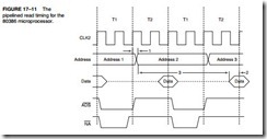
Figure 17–11 illustrates the read timing when the 80386 is operated in the pipelined mode. Notice that additional time is allowed to the memory for accessing data because the address is sent out early. Pipelined mode is selected by placing a logic 0 on the NA pin and by using address latches to capture the pipelined address. The clock pulse that is applied to the address
latches comes from the ADS signal. Address latches must be used with a pipelined system, as well as with interleaved memory banks. The minimum number of interleaved banks of two and four have been successfully used in some applications.
Notice that the pipelined address appears one complete clocking state before it normally appears with nonpipelined addressing. In the 16 MHz version of the 80386, this allows an additional 62.5 ns for memory access. In a nonpipelined system, a memory access time of 78 ns is allowed to the memory system; in a pipelined system, 140.5 ns is allowed. The advantages of the pipelined system are that no wait states are required (in many, but not all bus cycles) and much lower-speed memory devices may be connected to the microprocessor. The disadvantage is that we need to interleave memory to use a pipe, which requires additional circuitry and occasional wait states.
Wait States
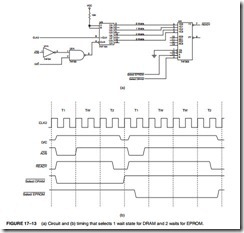
Wait states are needed if memory access times are long compared with the time allowed by the 80386 for memory access. In a nonpipelined 33 MHz system, memory access time is only 46 ns. Currently, only a few DRAM memories exist that have an access time of 46 ns. This means that often wait states must be introduced to access the DRAM (one wait for 60 ns DRAM) or an EPROM that has an access time of 100 ns (two waits). Note that this wait state is built into a motherboard and cannot be removed.
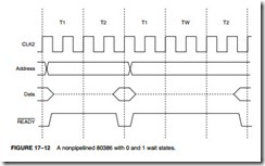
The READY input controls whether or not wait states are inserted into the timing. The READY input on the 80386 is a dynamic input that must be activated during each bus cycle. Figure 17–12 on the previous page shows a few bus cycles with one normal (no wait) cycle and one that contains a single wait state. Notice how the READY is controlled to cause 0 or 1 wait.
The READY signal is sampled at the end of a bus cycle to determine whether the clock cycle is T2 or TW. If READY 0 at this time, it is the end of the bus cycle or T2. If READY is 1 at the end of a clock cycle, the cycle is a TW and the microprocessor continues to test READY, searching for a logic 0 and the end of the bus cycle.
In the nonpipelined system, whenever ADS becomes a logic 0, a wait state is inserted if READY 1. After ADS returns to a logic 1, the positive edges of the clock are counted to generate the READY signal. The READY signal becomes a logic 0 after the first clock to insert 0 wait states. If one wait state is inserted, the READY line must remain a logic 1 until at least two clocks have elapsed. If additional wait states are desired, then additional time must elapse before READY is cleared. This essentially allows any number of wait states to be inserted into the timing.
Figure 17–13 on the previous page shows a circuit that inserts 0 through 3 wait states for various memory addresses. In the example, one wait state is produced for a DRAM access and two wait states for an EPROM access. The 74F164 clears whenever ADS is low and D>C is high. It begins to shift after ADS returns to a logic 1 level. As it shifts, the 00000000 in the shift register begins to fill with logic 1s from the QA connection toward the QH connection. The four different outputs are connected to an inverting multiplexer that generates the active low READY signal.

