I/O PORT ADDRESS DECODING
I/O port address decoding is very similar to memory address decoding, especially for memory- mapped I/O devices. In fact, we do not discuss memory-mapped I/O decoding because it is treated the same as memory (except that the IORC and IOWC are not used because there is no IN or OUT instruction). The decision to use memory-mapped I/O is often determined by the size of the memory system and the placement of the I/O devices in the system.
The main difference between memory decoding and isolated I/O decoding is the number of address pins connected to the decoder. We decode A31–A0, A23–A0, or A19–A0 for memory, and A15–A0 for isolated I/O. Sometimes, if the I/O devices use only fixed I/O addressing, we decode only A7–A0. In the personal computer system, we always decode all 16 bits of the I/O port address. Another difference with isolated I/O is that IORC and IOWC activate I/O devices for a read or write operation. On earlier versions of the microprocessor, IO>M 1 and RD or WR are used to activate I/O devices. On the newest versions of the microprocessor, the M>IO 0 and W>R are combined and used to activate I/O devices.
Decoding 8-Bit I/O Port Addresses
As mentioned, the fixed I/O instruction uses an 8-bit I/O port address that appears on A15–A0 as 0000H–00FFH. If a system will never contain more than 256 I/O devices, we often decode only address connections A7–A0 for an 8-bit I/O port address. Thus, we ignore address connection A15–A8. Embedded systems often use 8-bit port addresses. Please note that the DX register can also address I/O ports 00H–FFH. If the address is decoded as an 8-bit address, we can never include I/O devices that use a 16-bit I/O address. The personal computer never uses or decodes an 8-bit address.
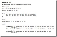
Figure 11–10 illustrates a 74ALS138 decoder that decodes 8-bit I/O ports F0H through F7H. (We assume that this system will only use I/O ports 00H–FFH for this decoder example.) This decoder is identical to a memory address decoder except we only connect address bits A7–A0 to the inputs of the decoder. Figure 11–11 shows the PLD version, using a GAL22V10 (a low-cost device) for this decoder. The PLD is a better decoder circuit because the number of integrated circuits has been reduced to one device. The VHDL program for the PLD appears in Example 11–2.
Decoding 16-Bit I/O Port Addresses
Personal computer systems typically use 16-bit I/O addresses. It is relatively rare to find 16-bit port addresses in embedded systems. The main difference between decoding an 8-bit I/O address and a 16-bit I/O address is that eight additional address lines (A15–A8) must be decoded. Figure 11–12 illustrates a circuit that contains a PLD and a 4-input NAND gate used to decode I/O ports EFF8H–EFFFH.
The NAND gate decodes part of the address (A15, A14, A13, and A11) because the PLD does not have enough address inputs. The output of the NAND gate connects to the Z input of the PLD and is decoded as a part of the I/O port address. The PLD generates address strobes for I/O ports EFF8H–EFFFH. The program for the PLD is listed in Example 11–3.
8- and 16-Bit Wide I/O Ports
Now that I/O port addresses are understood and we learned that an I/O port address is probably simpler to decode than a memory address (because of the number of bits), interfacing between the microprocessor and 8- or 16-bit-wide I/O devices is explained. Data transferred to an 8-bit I/O device exist in one of the I/O banks in a 16-bit microprocessor such as the 80386SX. There are 64K different 8-bit ports, but only 32K different 8-bit ports because a 16-bit port uses two 8-bit ports. The I/O system on such a microprocessor contains two 8-bit memory banks, just as memory does. This is illustrated in Figure 11–13, which shows the separate I/O banks for a 16-bit system such as the 80386SX.
Because two I/O banks exist, any 8-bit I/O write requires a separate write strobe to function correctly. I/O reads do not require separate read strobes. As with memory, the microprocessor reads only the byte it expects and ignores the other byte. The only time that a read can cause problems is when the I/O device responds incorrectly to a read operation. In the case of an I/O device that responds to a read from the wrong bank, we may need to include separate read signals. This is discussed later in this chapter.
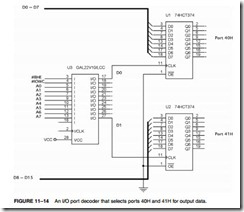
Figure 11–14 illustrates a system that contains two different 8-bit output devices, located at 8-bit I/O address 40H and 41H. Because these are 8-bit devices and because they appear in different I/O banks, separate I/O write signals are generated to clock a pair of latches that capture port data. Note that all I/O ports use 8-bit addresses. Thus, ports 40H and 41H can each be addressed as separate 8-bit ports, or together as one 16-bit port. The program for the PLD decoder used in Figure 11–14 is illustrated in Example 11–4.
When selecting 16-bit-wide I/O devices, the BLE (A0) and BHE pins have no function because both I/O banks are selected together. Although 16-bit I/O devices are relatively rare, a few do exist for analog-to-digital and digit-to-analog converters, as well as for some video and disk interfaces.
Figure 11–15 illustrates a 16-bit input device connected to function at 8-bit I/O addresses 64H and 65H. Notice that the PLD decoder does not have a connection for address bits BLE (A0) and BHE because these signals do not apply to 16-bit-wide I/O devices. The program for the PLD, illustrated in Example 11–5, shows how the enable signals are generated for the three-state buffers (74HCT244) used as input devices.
32-Bit-Wide I/O Ports
Although 32-bit-wide I/O ports are not common, they may eventually become commonplace because of newer buses found in computer systems. The once-promising EISA system bus supports 32-bit I/O as well as the VESA local and current PCI bus, but not many I/O devices are 32 bits in width.
The circuit of Figure 11–16 illustrates a 32-bit input port for the 80386DX through the 80486DX microprocessor. As with prior interfaces, this circuit uses a single PLD to decode the I/O ports and four 74HCT244 buffers to connect the I/O data to the data bus. The I/O ports decoded by this interface are the 8-bit ports 70H–73H, as illustrated by the PLD program in Example 11–6. Again, we only decode an 8-bit I/O port address. When writing software to access this port, it is crucial to use the address 70H for the 32-bit input as in the instruction IN EAX, 70H.
With the Pentium–Core2 microprocessors and their 64-bit data buses, I/O ports appear in various banks, as determined by the I/O port address. For example, 8-bit I/O port 0034H appears in Pentium I/O bank 4, while the l6-bit I/O ports 0034H–0035H appear in Pentium banks 4 and 5. A 32-bit I/O access in the Pentium system can appear in any four consecutive I/O banks. For example, 32-bit I/O ports 0100H–0103H appear in banks 0–3. The I/O address range must begin at a location where the rightmost two bits are zeros. Hence, 0100H–0103H is allowable but 0101H–0104H is not.
How is a 64-bit I/O device interfaced? The widest I/O transfers are 32 bits, and currently there are no 64-bit I/O instructions to support 64-bit transfers. This event is true for the Pentium 4 or Core2 operated in the 64-bit mode.
Suppose that we need to interface a simple 16-bit-wide output port at I/O port address 2000H and 2001H. The rightmost three bits of the lowest port address are 000 for port 2000H. This means that port 2000H is in memory bank 0. Likewise the rightmost three binary bits of I/O port 2001H are 001, which means that port 2001H is in bank 1. An interface is illustrated in Figure 11–17 and the PLD program is listed in Example 11–7.
The control signal M/IO and W/R must be combined to generate an I/O write signal for the latches and both BE0 and BE1 bank enable signals must be used to steer the write signal to the correct latch clock for address 2000H (bank 0) and 2001H (bank 1). The only problem that can arise in interfacing is when the I/O port spans across a 64-bit boundary, for example, a 16-bit- wide port located at 2007H and 2008H. In this case, port 2007H uses bank 7 and 2008H uses bank 0, but the address that is decoded is different for each location. A 0010 0000 0000 0XXX is decoded for 2007H and 0010 0000 0000 1XXX is decoded for 2008H. It is probably best to avoid situations such as this.


