BUS BUFFERING AND LATCHING
Before the 8086/8088 microprocessors can be used with memory or I/O interfaces, their multiplexed buses must be demultiplexed. This section provides the detail required to demultiplex the buses and illustrates how the buses are buffered for very large systems. (Because the maximum fan-out is 10, the system must be buffered if it contains more than 10 other components.)
Demultiplexing the Buses
The address/data bus on the 8086/8088 is multiplexed (shared) to reduce the number of pins required for the 8086/8088 microprocessor integrated circuit. Unfortunately, this burdens the hardware designer with the task of extracting or demultiplexing information from these multiplexed pins.
Why not leave the buses multiplexed? Memory and I/O require that the address remains valid and stable throughout a read or write cycle. If the buses are multiplexed, the address changes at the memory and I/O, which causes them to read or write data in the wrong locations.
All computer systems have three buses: (1) an address bus that provides the memory and I/O with the memory address or the I/O port number, (2) a data bus that transfers data between the micro- processor and the memory and I/O in the system, and (3) a control bus that provides control signals to the memory and I/O. These buses must be present in order to interface to memory and I/O.
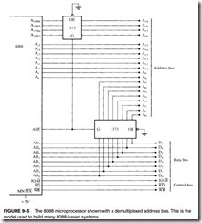
Demultiplexing the 8088. Figure 9–5 illustrates the 8088 microprocessor and the components required to demultiplex its buses. In this case, two 74LS373 or 74LS573 transparent latches are used to demultiplex the address/data bus connections AD7–AD0 and the multiplexed address/ status connections A19/S6–A16/S3.
These transparent latches, which are like wires whenever the address latch enable pin (ALE) becomes a logic 1, pass the inputs to the outputs. After a short time, ALE returns to its logic 0 condition, which causes the latches to remember the inputs at the time of the change to a
logic 0. In this case, A7–A0 are stored in the bottom latch and A19–A16 are stored in the top latch. This yields a separate address bus with connections A19–A0. These address connections allow the 8088 to address 1M byte of memory space. The fact that the data bus is separate allows it to be connected to any 8-bit peripheral device or memory component.
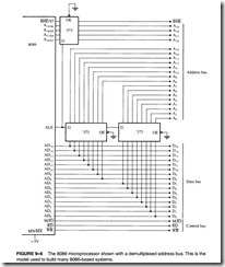
Demultiplexing the 8086. Like the 8088, the 8086 system requires separate address, data, and control buses. It differs primarily in the number of multiplexed pins. In the 8088, only AD7–AD0 and A19/S6–A16/S3 are multiplexed. In the 8086, the multiplexed pins include AD15–AD0 A19/S6–A16/S3, and BHE/S7. All of these signals must be demultiplexed.
Figure 9–6 illustrates a demultiplexed 8086 with all three buses: address (A19–A0 and BHE), data (D15–D0), and control (M>IO, RD, and WR).
This circuit shown in Figure 9–6 is almost identical to the one pictured in Figure 9–5, except that an additional 74LS373 latch has been added to demultiplex the address/data bus pins AD15–AD8 and a BHE/S7 input has been added to the top 74LS373 to select the high-order memory bank in the l6-bit memory system of the 8086. Here, the memory and I/O system see the
8086 as a device with a 20-bit address bus (A19–A0), a l6-bit data bus (D15–D0), and a three-line control bus (M>IO, RD, and WR).
The Buffered System
If more than 10 unit loads are attached to any bus pin, the entire 8086 or 8088 system must be buffered. The demultiplexed pins are already buffered by the 74LS373 or 74LS573 latches, which have been designed to drive the high-capacitance buses encountered in microcomputer systems. The buffer’s output currents have been increased so that more TTL unit loads may be driven: A logic 0 output provides up to 32 mA of sink current, and a logic 1 output provides up to 5.2 mA of source current.
A fully buffered signal will introduce a timing delay to the system. This causes no difficulty unless memory or I/O devices are used, which function at near the maximum speed of the bus. Section 9–4 discusses this problem and the time delays involved in more detail.
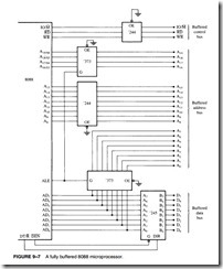
![]() The Fully Buffered 8088. Figure 9–7 depicts a fully buffered 8088 microprocessor. Notice that the remaining eight address pins, A15–A8, use a 74LS244 octal buffer; the eight data bus pins, D7–D0, use a 74LS245 octal bidirectional bus buffer; and the control bus signals, M>IO, RD,
The Fully Buffered 8088. Figure 9–7 depicts a fully buffered 8088 microprocessor. Notice that the remaining eight address pins, A15–A8, use a 74LS244 octal buffer; the eight data bus pins, D7–D0, use a 74LS245 octal bidirectional bus buffer; and the control bus signals, M>IO, RD,
and WR, use a 74LS244 buffer. A fully buffered 8088 system requires two 74LS244s, one 74LS245, and two 74LS373s. The direction of the 74LS245 is controlled by the DT/R signal and is enabled and disabled by the DEN signal.
The Fully Buffered 8086. Figure 9–8 illustrates a fully buffered 8086 microprocessor. Its address pins are already buffered by the 74LS373 address latches; its data bus employs two
74LS245 octal bidirectional bus buffers; and the control bus signals, M>IO, RD, and WR use a 74LS244 buffer. A fully buffered 8086 system requires one 74LS244, two 74LS245s, and three 74LS373s. The 8086 requires one more buffer than the 8088 because of the extra eight data bus connections, D15–D8. It also has a BHE signal that is buffered for memory-bank selection.


