Interfacing Devices Memory Devices and Interfacing Interfacing Devices
Any application of a microprocessor based system requires the transfer of data between external circuitry to the microprocessor and microprocessor to the external circuitry. Most of the peripheral devices are designed and interfaced with a CPU either to enable it to communicate with the user or an external process and to ease the circuit operations so that the microprocessor works more efficiently .
The use of peripheral integrated devices simplifies both the hardware circuits and software considerable. The following are the devices used in interfacing of Memory and General I/O devices
• 74LS138 (Decoder / Demultiplexer).
• 74LS373 / 74LS374 3-STATE Octal D-Type Transparent Latches.
• 74LS245 Octal Bus Transceiver: 3-State.
74LS138 (Decoder / Demultiplexer)
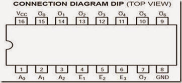
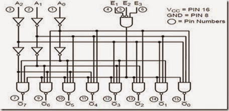
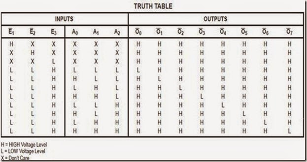
The LS138 is a high speed 1-of-8 Decoder/Demultiplexer fabricated with the low power Schottky barrier diode process. The decoder accepts three binary weighted inputs (A0, A1, A2) and when enabled provides eight mutually exclusive active LOW Outputs (O0–O7).
The LS138 can be used as an 8-output demultiplexer by using one of the active LOW Enable inputs as the data input and the other Enable inputs as strobes. The Enable inputs which are not used must be permanently tied to their appropriate active HIGH or active LOW state.
74LS138 (Decoder / Demultiplexer)
• Demultiplexing Capability
• Multiple Input Enable for Easy Expansion
• Typical Power Dissipation of 32 mW
• Active Low Mutually Exclusive Outputs
Logic Diagram of 74138
Truth Table of 74138
74LS373 / 74LS374 3-STATE Octal D-Type Transparent Latches and Edge- Triggered Flip-Flops
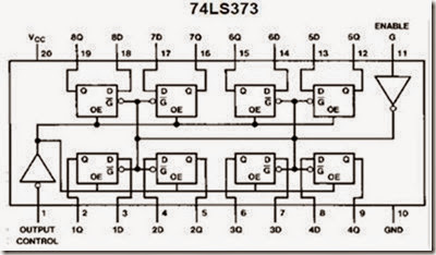
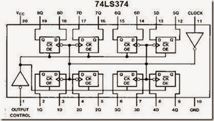
These 8-bit registers feature totem-pole 3-STATE outputs designed specifically for implementing buffer registers, I/O ports, bidirectional bus drivers, and working registers. The eight latches of the 74LS373 are transparent Dtype latches meaning that while the enable (G) is HIGH the Q outputs will follow the data (D) inputs.
When the enable is taken LOW the output will be latched at the level of the data that was set up. The eight flip-flops of the 74LS374 are edge-triggered D-type flip flops. On the positive transition of the clock, the Q outputs will be set to the logic states that were set up at the D inputs.
Main Features
• Choice of 8 latches or 8 D-type flip-flops in a single package
• 3-STATE bus-driving outputs
• Full parallel-access for loading
• Buffered control inputs
• P-N-P inputs reduce D-C loading on data lines
Connection Diagram of 74LS373
Connection Diagram of 74LS374
74LS245 Octal Bus Transceiver: 3-State
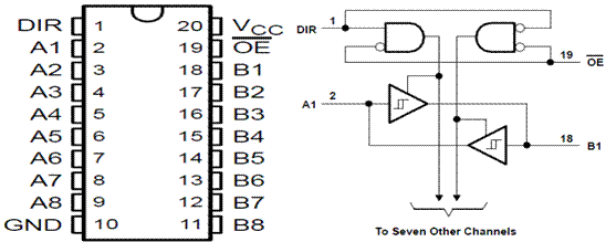
The 74LS245 is a high-speed Si-gate CMOS device. The 74LS245 is an octal transceiver featuring non-inverting 3-state bus compatible outputs in both send and receive directions. The 74LS245 features an Output Enable (OE) input for easy cascading and a send/receive (DIR) input for direction control. OE controls the outputs so that the buses are effectively isolated. All inputs have a Schmitt-trigger action.
These octal bus transceivers are designed for asynchronous two-way communication between data buses. The 74LS245 is a high-speed Si-gate CMOS device. The 74LS245 is an octal transceiver featuring non-inverting 3-state bus compatible outputs in both send and receive directions.
The 74LS245 features an Output Enable (OE) input for easy cascading and a send/receive (DIR) input for direction control. OE controls the outputs so that the buses are effectively isolated. All inputs have a Schmitt-trigger action. These octal bus transceivers are designed for asynchronous two-way communication between data buses.
Pin diagram of 74LS245 Logic diagram (Positive Logic)
Memory Devices And Interfacing
The memory interfacing circuit is used to access memory quit frequently to read instruction codes and data stored in the memory. The read / write operations are monitored by control signals. Semiconductor memories are of two types. Viz. RAM (Random Access Memory) and ROM (Read Only Memory) The Semiconductor RAM’s are broadly two types- static Ram and dynamic RAM
Memory structure and its requirements
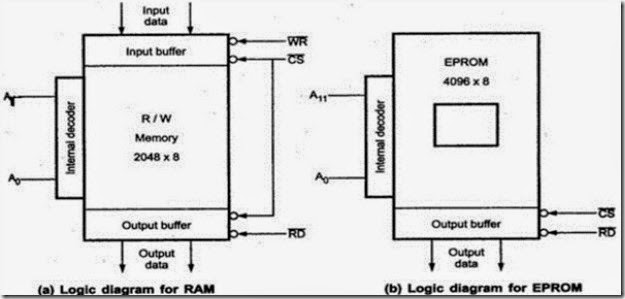
The read / write memories consist of an array of registers in which each register has unique address. The size of memory is N * M as shown in figure.
Where N is number of register and M is the word length, in number of bits. As shown in figure(a) memory chip has 12 address lines Ao–A11, one chip select (CS), and two control lines, Read (RD) to enable output buffer and Write (WR) to enable the input buffer.
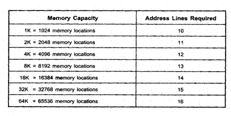
The internal decoder is used to decoder the address lines. Figure(b) shows the logic diagram of a typical EPROM (Erasable Programmable Read-Only Memory) with 4096 (4K) register. It has 12 address lines Ao – A11, one chip select (CS), one read control signal. Since EPROM does not require the (WR) signal. The Following Table Summarizes the Memory Capacity and Address Lines required for Memory Interfacing.
Example :
If memory is having 12 address lines and 16 data lines, then Number of registers / memory locations = 2 ^ N = 2 ^ 12
= 4096
Word length = M bits
= 16 bits
Basic Concepts in memory interfacing
For interfacing memory devices to microprocessor 8086 following important points are to be kept in mind. Microprocessor 8086 can access 1 Mbytes memory since address bus is 20-bit. But it is not always necessary to use full 1 Mbytes address space. The total memory space depends upon the application.
Generally EPROM (or EPROMs) is used as a program memory and RAM (or RAMs) as a data memory. When both, EPROM and RAM are used, the total address space 1 Mbytes is shared by them.
The individual capacities of program memory and data memory depends on the application. It is not always necessary to select 1 EPROM and 1 RAM. We can have multiple EPROMs and multiple RAMs as per the requirement of application. We can place EPROM/RAM anywhere in full 1 Mbytes address space. But program memory (EPROM) should be located at last memory page so that the starting address FFFF0H will lie within the program memory range.
To provide facility to set addresses in the interrupt vector table we must provide RAM at page 0 of memory. So that the interrupt vector table lie with the read/write memory range. It is not always necessary to locate EPROM and RAM in consecutive memory
addresses. However, it is advised to do that. While interfacing memory to 8086 we have to provide odd and even banks of memory. Even banks is selected when Ao = 0 and odd bank is selected when BHE = 0.
The Memory Interfacing requires to :
• Select the chip
• Identify the register
• Enable the appropriate buffer
Address Decoding Techniques
• Absolute decoding
• Linear decoding
• Block decoding
Absolute Decoding :
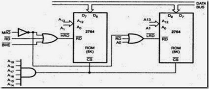
In the absolute decoding technique the memory chip is selected only for the specified logic level on the address lines: no other logic levels can select the chip. Below figure the memory interface with absolute decoding. Two 8K EPROMs (2764) are used to provide even and odd memory banks.
Control signals BHE and Ao are use to enable output of odd and even memory banks respectively. As each memory chip has 8K memory locations, thirteen address lines are required to address each locations, independently. All remaining address lines are used to generate an unique chip select signal. This address technique is normally used in large memory systems.
Linear Decoding :
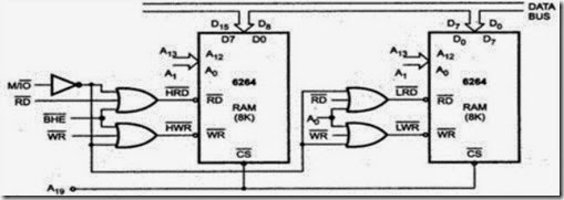
In small system hardware for the decoding logic can be eliminated by using only required number of addressing lines (not all). Other lines are simple ignored. This technique is referred as linear decoding or partial decoding. Control signals BHE and Ao are used to enable odd and even memory banks, respectively. Figure shows the addressing of 16K RAM (6264) with linear decoding.
The address line A19 is used to select the RAM chips. When A19 is low, chip is selected, otherwise it is disabled. The status of A14 to A18 does not affect the chip selection logic. This gives you multiple addresses (shadow addresses). This technique reduces the cost of decoding circuit, but it gas drawback of multiple addresses.
Block Decoding :
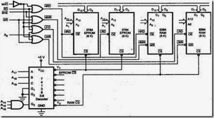
In a microcomputer system the memory array is often consists of several blocks of memory chips. Each block of memory requires decoding circuit. To avoid separate decoding for each memory block special decoder IC is used to generate chip select signal for each block.
Figure shows the Block decoding technique using 74138, 3:8 decoder
