MAPPING AN ALGORITHM ONTO A PARALLEL ARCHITECTURE
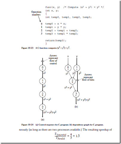
The process of mapping an algorithm onto a parallel architecture begins with a dependency analysis in which data dependencies among the operations in a program are identified. Consider the C code shown in Figure 10-23. In an ordinary SISD processor, the four numbered statements require four time steps to
complete, as illustrated in the control sequence of Figure 10-24a. The dependency graph shown in Figure 10-24b exposes the natural parallelism in the control sequence. The dependency graph is created by assigning each operation in the original program to a node in the graph, and then drawing a directed arc from each node that produces a result to the node(s) that needs it.
The control sequence requires four time steps to complete, but the dependency graph shows that the program can be completed in just three time steps, since operations 0 and 1 do not depend on each other and can be executed simulta-
may not be very great, but for other programs, the opportunity for speedup can be substantial as we will see.
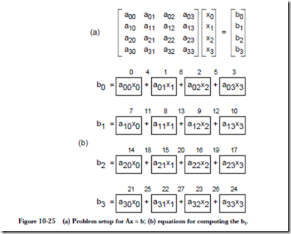
Consider a matrix multiplication problem Ax = b in which A is a 4´4 matrix and x and b are both 4´1 matrices, as illustrated in Figure 10-25a. Our goal is to
solve for the bi, using the equations shown in Figure 10-25b. Every operation is assigned a number, starting from 0 and ending at 27. There are 28 operations, assuming that no operations can receive more than two operands. A program running on a SISD processor that computes the bi requires 28 time steps to complete, if we make a simplifying assumption that additions and multiplications take the same amount of time.
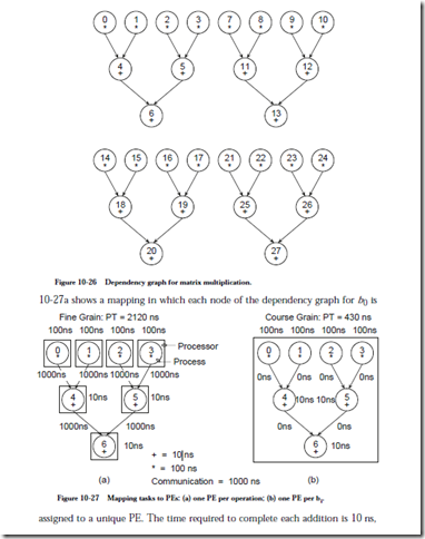
A dependency graph for this problem is shown in Figure 10-26. The worst case path from any input to any output traverses three nodes, and so the entire process can be completed in three time steps, resulting in a speedup of
Now that we know the structure of the data dependencies, we can plan a map- ping of the nodes of the dependency graph to PEs in a parallel processor. Figure
the time to complete each multiplication is 100 ns, and the time to communicate between PEs is 1000 ns. These numbers are for a fictitious processor, but the methods extend to real parallel processors.
As we can see from the parallel time of 2120 ns to execute the program using the mapping shown in Figure 10-27a, the time spent in communication dominates performance. This is worse than a SISD approach, since the 16 multiplications and the 12 additions would require 16 ´ 100 ns + 12 ´ 10 ns = 1720 ns. There is no processor-to-processor communication cost within a SISD processor, and so only the computation time is considered.
An alternative mapping is shown in Figure 10-27b in which all of the operations needed to compute b0 are clustered onto the same PE. We have thus increased the granularity of the computation, which is a measure of the number of operations assigned to each PE. A single PE is a sequential, SISD processor, and so none of the operations within a cluster can be executed in parallel, but the communication time among the operations is reduced to 0. As shown in the diagram, the parallel time for b0 is now 430 ns which is much better than either the previous parallel mapping or a straight SISD mapping. Since there are no dependencies among the bi, they can all be computed in parallel, using one processor per bi. The actual speedup is now:
Communication is always a bottleneck in parallel processing, and so it is important that we maintain a proper balance. We should not be led astray into thinking that adding processors to a problem will speed it up, when in fact, adding processors can increase execution time as a result of communication time. In general, we want to maintain a ratio in which: ![]()
FINE-GRAIN PARALLELISM – THE CONNECTION MACHINE CM-1
The Connection Machine (CM-1) is a massively parallel SIMD processor designed and built by Thinking Machines Corporation during the 1980’s. The architecture is noted for high connectivity between a large number of small processors. The CM-1 consists of a large number of one-bit processors arranged at the vertices of an n-space hypercube. Each processor communicates with other processors via routers that send and receive messages along each dimension of the hypercube.
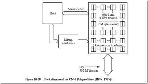
A block diagram of the CM-1 is shown in Figure 10-28. The host computer is a
conventional SISD machine such as a Symbolics computer (which was popular at the time) that runs a program written in a high level language such as LISP or
C. Parallelizeable parts of a high level program are farmed out to 2n processors (216 processors is the size of a full CM-1) via a memory bus (for data) and a microcontroller (for instructions) and the results are collected via the memory bus. A separate high bandwidth datapath is provided for input and output directly to and from the hypercube.
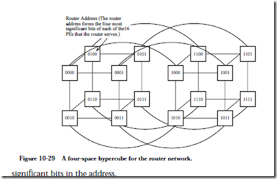
The CM-1 makes use of a 12-space hypercube between the routers that send and receive data packets. The overall CM-1 prototype uses a 16-space hypercube, and so the difference between the 12-space router hypercube and the 16-space PE hypercube is made up by a crossbar that serves the 16 PEs attached to each router. For the purpose of example, a four-space hypercube is shown in Figure 10-29 for the router network. Each vertex of the hypercube is a router with an attached group of 16 PEs, each of which has a unique binary address. The router hypercube shown in Figure 10-29 thus serves 256 PEs. Routers that are directly connected to other routers can be found by inverting any one of the four most Router Address (The router address forms the four most significant bits of each of the16 PEs that the router serves.)
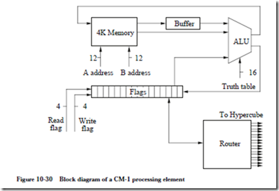
Each PE is made up of a 16-bit flag register, a three-input, two-output ALU, and a 4096-bit random access memory, as shown in Figure 10-30. During operation,
an external controller (the microcontroller of Figure 10-28) selects two bits from memory via the A address and B address lines. Only one value can be read from memory at a time, so the A value is buffered while the B value is fetched. The controller selects a flag to read, and feeds the flag and the A and B values into an ALU whose function it also selects. The result of the computation produces a new value for the A addressed location and one of the flags.
The ALU takes three one-bit data inputs, two from the memory and one from the flag register, and 16 control inputs from the microcontroller and produces two one-bit data outputs for the memory and flag registers. The ALU generates all 23 = 8 combinations (minterms) of the input variables for each of the two outputs. Eight of the 16 control lines select the minterms that are needed in the sum-of-products form of each output.
PE’s communicate with other PE’s through routers. Each router services communication between a PE and the network by receiving packets from the network intended for the attached PEs, injecting packets into the network, buffering when necessary, and forwarding messages that use the router as an intermediary to get to their destinations.
The CM-1 is a landmark machine for the massive parallelism made available by the architecture. For scalable problems like finite element analysis (such as modeling heat flow through the use of partial differential equations), the avail- able parallelism can be fully exploited. There is usually a need for floating point manipulation for this case, and so floating point processors augment the PEs in the next generation CM-2. A natural way to model heat flow is through a mesh interconnect, which is implemented as a hardwired bypass to the message-pass- ing routing mechanism through the North-East-West-South (NEWS) grid. Thus we can reduce the cost of PE-to-PE communication for this application.
Not all problems scale so well, and there is a general trend moving away from fine grain parallel processing. This is largely due to the difficulty of keeping the PEs busy doing useful work, while also keeping the time spent in computation greater than the time spent in communication. In the next section, we look at a coarse grain architecture: The CM-5.
COURSE-GRAIN PARALLELISM: THE CM-5
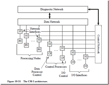
The CM-5 (Thinking Machines Corporation) combines properties of both SIMD and MIMD architectures, and thereby provides greater flexibility for mapping a parallel algorithm onto the architecture. The CM-5 is illustrated in Figure 10-31. There are three types of processors for data processing, control, and I/O. These processors are connected primarily by the Data Network and the Control Network, and to a lesser extent by the Diagnostic Network.
The processing nodes are assigned to control processors, which form partitions, as illustrated in Figure 10-32. A partition contains a control processor, a number
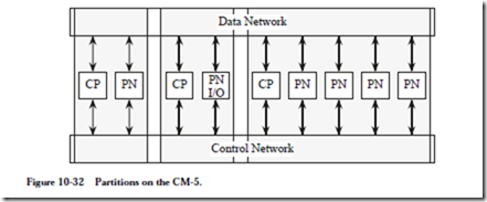 of processing nodes, and dedicated portions of the Control and Data Networks. Note that there are both user partitions (where the data processing takes place) and I/O partitions.
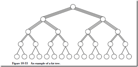
The Data Network uses a fat-tree topology, as illustrated in Figure 10-33. The general idea is that the bandwidth from child nodes to parent nodes increases as
the network approaches the root, to account for the increased traffic as data travels from the leaves toward the root.
The Control Network uses a simple binary tree topology in which the system components are at the leaves. A control processor occupies one leaf in a partition, and the processing nodes are placed in the remaining nodes, although not necessarily filling all possible node positions in a subtree.
The Diagnostic Network is a separate binary tree in which one or more diagnostic processors are at the root. At the leaves are physical components, such as circuit boards and backplanes, rather than logical components such as processing nodes.
Each control processor is a self-contained system that is comparable in complexity to a workstation. A control processor contains a RISC microprocessor that serves as a CPU, a local memory, I/O that contains disks and Ethernet connections, and a CM-5 interface.
Each processing node is much smaller, and contains a SPARC-based microprocessor, a memory controller for 8, 16, or 32 Mbytes of local memory, and a net- work interface to the Control and Data Networks. In a full implementation of a CM-5, there can be up to 16,384 processing nodes, each performing 64-bit floating point and integer operations, operating at a clock rate of 32 MHz.
Overall, the CM-5 provides a true mix of SIMD and MIMD styles of processing, and offers greater applicability than the stricter SIMD style of the CM-1 and CM-2 predecessors.
