11.3.5 80386 Pins and Signals
The 80386 contains 132 pins in Pin Grid Array (PGA) or other packages.
Figure 11.2 shows functional grouping of the 80386 pins. A brief description of the 80386 pins and signals is provided in the following. The # symbol at the end of the signal name or the- symbol above a signal name indicates the active or asserted state when it is low. When the symbol # is absent after the signal name or the symbol- is absent above a signal name, the signal is asserted when high.
The 80386 has 20 Vcc and 21 GND pins for power distribution. These multiple power and ground pins reduce noise. Preferably, the circuit board should contain VCC and GND planes.
CLK2 pin provides the basic timing for the 80386. This clock is then divided by 2 by the 80386 internally to provide the clock used for instruction execution. The 80386 is reset by activating the RESET pin for at least 15 CLK2 periods. The RESET signal is level sensitive. When the RESET pin is asserted, the 80386 will start executing instructions at address FFFF FFF0H. The 82384 clock generator provides system clock and reset signals.
D0-D31 provides the 32-bit data bus. The 80386 can transfer 16- or 32-bit data via the data bus.
The address pins A2-A31 along with the byte enable signals BEO# through BE3# are used to generate physical memory or I/O port addresses. Using the pins, the 80386 can directly address 4 gigabytes by physical memory (00000000H through FFFFFFFFH).
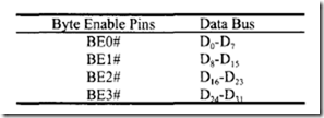
The byte enable outputs, BE0# through BE3# of the 80386, define which bytes of D0-D31 are utilized in the current data transfer. These definations are given below:
The 80386 asserts one or more byte enables depending on the physical size of the operand being transferred (1, 2, 3, or 4 bytes).
W/R#, D/C#, M/IO#, and LOCK# output pins specify the type of bus cycle being performed by the 80386. W/R# pin, when HIGH, identifies write cycle and, when LOW, indicates read cycle. D/C# pin, when HIGH, identifies data cycle, when LOW, indicates control cycle. M/ lO# differentiates between memory and I/O cycles. LOCK# distinguishes between locked and unlocked bus cycles. W/R#, DIC#, and M/10# pins define the primary bus cycle. This is because these signals are valid when ADS# (address status output) is asserted. Some of these bus cycles are listed below.
The 80386 bus control signals include ADS# (address status), READY# (transfer acknowledge), NA# (next address request), and BS16# (bus size 16).
The 80386 outputs LOW on the ADS# pin indicate a valid bus cycle (W!R#, Dl C#, M/lO#) and bus enable I address (BEO#-BE3#, A2-A31) signals.
When READY# input is LOW during a read cycle or an interrupt acknowledge cycle, the 80386latches the input data on the data pins and ends the cycle. When READY# is low during a write cycle, the 80386 ends the bus cycle.
The NA# input pin is activated low by external hardware to request address pipelining. BS 16# input pin permits the 80386 to interface to 32- and 16-bit memory or I/O. For 16-bit memory or 1/0, BS16# input pin is asserted low by an external device, the 80386 uses the low-order half (D0-D15) of the data bus corresponding to BEO# and BE 1# for data transfer.
BS16# is asserted high for 32-bit memory or I/O. HOLD (input) and HLDA (output) pins are 80386 bus arbitration signals. These signals are used for DMA transfers. PEREQ, BUSY#, and ERROR# pins are used for interfacing coprocessors such as 80287 or 80387 to the 80386.
There are two interrupt pins or the 80386. These are INTR (maskable) and NMI (nonmaskable) pins. NMI is leading-edge sensitive, whereas INTR is level-sensitive. When INTR is asserted and if the IF bit in the EFLAGS is 1, the 80386 (when ready) responds to the INTR by performing two interrupt acknowledge cycles and at the end of the second cycle latches an 8-bit vector on D0-D7 to identify the source of interrupt. Interrupts are serviced in a similar manner as the 8086.
11.3.6 80386 Modes
As mentioned before, the 80386 can be operated in real, protected, or virtual 8086 mode. These modes can be selected by some of the bits in the status register. Upon reset or power-up, the 80386 operates in real mode. In real mode, the 80386 can access all the 8086 registers along with the 80386 32-bit register. In real mode, the 80386 can directly address up to one megabyte of memory. The address lines A2-A 19, BEO#-BE3# are used by the 80386 in this mode.
The protected mode provides more memory space than is provided by the real mode. Furthermore, this mode supports on-chip memory management and protection features along with a multitasking operating system. Finally, the virtual 8086 mode permits the execution of8086 programs, taking full advantage of the 80386 protection mechanism. In particular, the virtual the 8086 mode allows execution of 8086 operating system and application programs concurrently with the 80386 operating system and application programs.
11.3.8 80386 System Design
In this section, the 80386 is interfaced to typical EPROM chips. As mentioned in the last section the 80386 address and data lines are not multiplexed. There is a total of thirty address pins (A2-A31) on the chip. A0 and A 1 are decoded internally to generate four byte enable outputs, BEO#, BEl#, BE2#, and BE3#. In real mode, the 80386 utilizes 20-bit addresses and A2 through A 19 address pins are active and the address pins A20 through A31 are used in real mode at reset, high for code segment (CS)-based accesses, low for others, and always low after CS changes. In the protected mode, on the other hand, all address pins A2 through A31 are active. In both modes, A0 and A 1 are obtained internally. In all modes, the 80386 outputs on the byte enable pins to activate appropriate portions of the data to transfer byte (8-bit), word ( 16-bit), and double-word (32-bit) data as follows:
The 80386 supports dynamic bus sizing. This feature connects the 80386 with 32- bit or 16-bit data busses for memory or I/O. The 80386 32-bit data bus can be dynamically switched to a 16-bit bus by activating the BS 16# input from high to low by a memory or I/O device. In this case, all data transfers are performed via D0-D15 pins. 32-bit transfers take place as two consecutive 16-bit transfers over data pins D0 through D15• On the other hand, the 32-bit memory or I/O device can activate the BS 16# pin HIGH to transfer data over D0-D31 pins.
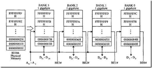
The 80386 address pins A 1 and A0 specify the four addresses of a four byte (32- bit) word. Consider the following:
The contents of the memory addresses which include 0, 4, 8, … with A 1A0 = 002 are transferred over D0-D7 • Similarly, the contents of addresses which include 1,5,9, …, with A 1A0 = 012 are transferred over D15 -D8• On the other hand, the contents of memory addresses 2, 6, 10, … with A 1A0 = 102 are transferred over D16-D23 while contents of addresses 3, 7, 11 … with A 1A0 = 112 are transferred over D24-D31 • Note that A 1A0 is encoded from BE3# -BEO#. The following figure depicts this:
In each bank, a byte can be accessed by enabling one of the byte enables, BEO# -BE3#. For example, in response to execution of a byte-MOVE instruction such as MOV [00000006H], BL, the 80386 outputs low on BE2# and high on BEO#, BEl# and BE3# and the content of BL is written to address 00000006H. On the other hand, when the 80386 executes a MOVE instruction such as MOV [ 00000004H], AX, the 80386 drives BEO# and BEl# to low. The locations 00000004H and 00000005H are written with the contents of ALand AH via D0-D7 and D8-D 15 respectively. For 32-bit transfer, the 80386 executing a MOVE instruction from an aligned address such as MOV [ 00000004H], EAX, drives all bus enable pins (BEO# -BE3#) to low and writes four bytes to memory locations 00000004H through 00000007H from EAX. Byte (8-bit), aligned word (16-bit), and aligned double-word (32-bit) are transferred by the 80386 in a single bus cycle.
The 80386 performs misaligned transfers in multiple cycles. For example, the 80386 executing a misaligned word MOVE instruction such as MOV [ 0 0 0 0 0 0 0 3H] ,AX drives BE3# to low in the first bus cycle and writes into location 00000003H (bank 3) from AL in the first bus cycle. The 80386 then drives BEO# to low in the second bus cycle and writes into location 00000004H (bank 0) from AH. This transfer takes two bus cycles.
A 32-bit misaligned transfer such as MOV [ 00000002H], EAX, on the other hand, takes two bus cycles. In the first bus cycle, the 80386 enables BE2# and BE3#, and writes the contents of low 16-bits of EAX into addresses 00000002H and 00000003H from banks 2 and 3 respectively. In the second cycle, the 80386 enables BEO# and BEl# to low and then writes the contents of upper 16-bits of EAX into addresses 00000004H and 00000005H.
In the following, design concepts associated with the 80386’s interface to memory will be discussed. The 80386 device will use 128 Kbyte, 32-bit wide memory. Four 27C256’s (32 K x 8 HCMOS EPROMs) are used.
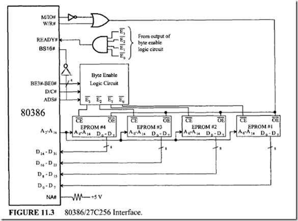
Since the 27C256 chip is 32K x 8 chip, the 80386 address lines A2-A 16 are used for addressing the 27C256’s. The 80386 M/10#, D/C#, W/R#, and BEO#-BE3# are also used. Figure 11.3 shows a simplified 80386 – 27C256 interface.
In figure 11.3, A 1 A0,BE3#-BEO#, D/C#, and ADS# pins of the 80386 are used to generate four byte enable signals, EO, E 1, E2, and E3.
The 80386 outputs low on ADS# (Address status) pin to indicate valid bus cycle (W/R#, D/C#, M/10#) and address (BEO# -BE3#) signals.
The 80386 A 1 and A0 bits (obtained internally) indicate which portion of the data bus will be used to transfer data. For example, A 1 A0 = 11 means that contents of addresses
such as 00000003H, 00000007H, … will be used by the 80386 to transfer data via its D31 -D24 pins. BE3#-BEO# and D/C# are used to produce the byte enable signals which
are connected to the CE pin of the appropriate EPROM. The inverted M/IO# is logically ORed with the W/R# pin. The output of this OR gate is connected to the OE pin of all four EPROM’s.
![]() EO, El, E2, and E3 are AND ed and connected to the READY# pin. When the READY# pin is asserted LOW, the 80386latches or reads data. Until READY# pin is asserted LOW by the external device, the 80386 inserts wait states. One must ensure that the data is ready before READY# is asserted. The BS 16# is asserted HIGH by connecting it to inverted ADS# to indicate 32-bit memory. NA# is connected to +5 V to disable pipelining.
EO, El, E2, and E3 are AND ed and connected to the READY# pin. When the READY# pin is asserted LOW, the 80386latches or reads data. Until READY# pin is asserted LOW by the external device, the 80386 inserts wait states. One must ensure that the data is ready before READY# is asserted. The BS 16# is asserted HIGH by connecting it to inverted ADS# to indicate 32-bit memory. NA# is connected to +5 V to disable pipelining.
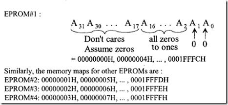
The memory map can be determined as follows:
11.3.9 80386 I/O
The 80386 can use either a standard I/O or a memory-mapped I/O technique.
The address decoding required to generate chip selects for devices using standard I/O is often simpler than that required for memory-mapped devices. But, memory-mapped I/O offers more flexibility in protection than standard I/O does.
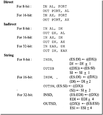
The 80386 can operate with 8-, 16-, and 32-bit peripherals. Eight-bit I/O devices can be connected to any of the four 8-bit sections of the data bus. For efficient operation, 32-bit 1/0 devices should be assigned to addresses that are even multiples of four. For standard 1/0, the 80386 includes there types of I/O instructions. These are direct, indirect, and string I/O instructions which include the following:

