10.10 68000 Memory Interface
![]() One of the advantages of the 68000 is that it can easily be interfaced to memory chips with various speeds because it goes into a wait state if DTACK is not asserted (LOW) by the memory devices at the end of S4. A simplified schematic showing an interface of a 68000 to two 2732’s and two 6116’s is given in Figure 10.15. As mentioned in Chapter 9, the 2732 is a 4K x 8 EPROM and the 6116 is a 2K x 8 static RAM. The pin diagrams of the 6116 and 2732 are provided in Appendices C and E respectively. For a 4-MHz clock, each cycle is 250 ns. Because the 68000 samples data at the falling edge of S4 (750 ns) and latches data at the falling edge of S6 (1000 ns), AS can be used to assert DTACK. From the 68000 timing diagram of Figure 10.13, AS goes to LOW after approximately two cycles (500 ns). The time delay between AS going LOW and the falling edge of S6 is 500 ns. Note that LDS and UDS must be used as chip selects as in Figure 10.15. They must not be connected to AO of the memory chips. Because in that case half of the memory in each memory chip would be wasted. Note that LDS and UDS also go to LOW after about two cycles (500 ns).
One of the advantages of the 68000 is that it can easily be interfaced to memory chips with various speeds because it goes into a wait state if DTACK is not asserted (LOW) by the memory devices at the end of S4. A simplified schematic showing an interface of a 68000 to two 2732’s and two 6116’s is given in Figure 10.15. As mentioned in Chapter 9, the 2732 is a 4K x 8 EPROM and the 6116 is a 2K x 8 static RAM. The pin diagrams of the 6116 and 2732 are provided in Appendices C and E respectively. For a 4-MHz clock, each cycle is 250 ns. Because the 68000 samples data at the falling edge of S4 (750 ns) and latches data at the falling edge of S6 (1000 ns), AS can be used to assert DTACK. From the 68000 timing diagram of Figure 10.13, AS goes to LOW after approximately two cycles (500 ns). The time delay between AS going LOW and the falling edge of S6 is 500 ns. Note that LDS and UDS must be used as chip selects as in Figure 10.15. They must not be connected to AO of the memory chips. Because in that case half of the memory in each memory chip would be wasted. Note that LDS and UDS also go to LOW after about two cycles (500 ns).
In Figure 10.15, a delay circuit for DTACK is not required because the 2732 and 6116 both place data on the bus lines before the 68000 latches data. This is because the 68000 clock frequency is 4 MHz in this case. Thus, each clock cycle is 250 ns. The access times of the 2732 and 6116 are 200 ns and 120 ns respectively. Because DTACK is sampled after 3 clock cycles (3 x 250 ns = 750 ns), both the 2732 and 6116 will have adequate time to place data on the bus for the 68000 to latch.
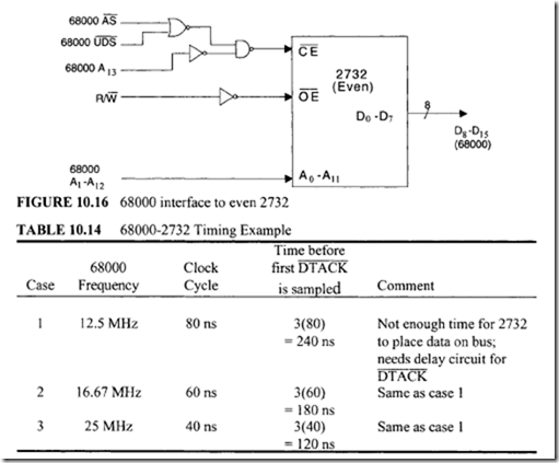
For example, consider the even 2732 EPROM of Figure 10.16. UDS and AS are NORed and then NANDed with inverted A 13 to select this chip. With the 200-ns access time of the 2732 (Used to be 450ns), data will be placed on the 68000 D8-D15 pins after approximately 720 nanoseconds (500 ns for AS or UDS + 10 ns for the NOR gate+ 10 ns for the NAND gate+ 200 ns for the 2732). Therefore, no delay circuit for the 68000 DTACK
is required because the 68000 latches data from the D8-D15 pins after 4 cycles (1000 ns in this case). The timing parameters of the 68000-2732 with various 68000 frequencies are shown in Table 10.14.
Next, consider odd 6116 static RAM (SRAM) with a 4-MHz 68000. Note that the 6116 signals, W (Write enable), G (Output enable), and E (Chip enable) are decoded as follows: when G = 0 and E = 0, then W = 1 for read and W = 0 for write. In this case, LDS and AS are NORed and NANDed with A 13 to select this chip. With the 120-ns access time of the 6116 RAM, data will be placed on the 68000 D0-D7 pins after approximately 640 ns. Because the 68000 latches data after four cycles (1000 ns in this case), no delay circuit for DTACK is required. The requirements for DTACK for 68000/6116 for various 68000 clock frequencies can similarly be determined.
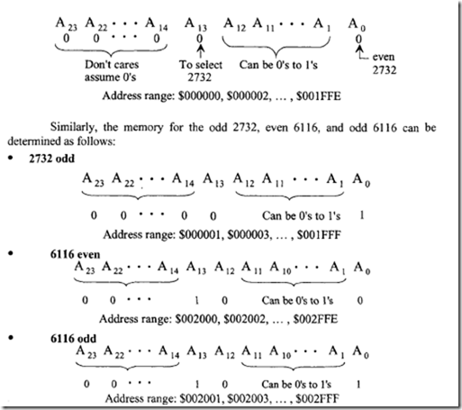
In case a delay circuit for DTACK is required, a ring counter with D flip-flops can be used. Let us now determine the memory maps. Figure I 0.16 shows the 68000 interface to even 2732 obtained from Figure 10.15. When A 13 = 0, UDS = 0, AS= 0, and R/W =1, the 2732 will be selected by the 68000 to read data from the 68000 DcD 15 pins. The 68000 address pins A23-A 14 are D0n’t cares (assume 0). The memory map for the even 2732 can be determined as follows:
In the above, for 6116’s, A 12 and A 14 – A23 are Don’t cares (assume O’s). Static RAMs such as 6116 are used for small memory system. Note that RAMs are needed when subroutines and interrupts requiring stack are desired in an application. Microprocessors requiring larger RAMs use dynamic RAMs (DRAMs). Concepts associated with interfacing DRAMs to 68000 will be discussed next.
DRAMs are typically used when memory requirements are 16k words or larger. DRAM is addressed via row and column addressing. For example, one megabit DRAM requiring 20 address bits is addressed using I 0 address lines and two control lines, RAS (Row Address Strobe) and CAS ( Column Address Strobe). To provide a 20-bit address into the DRAM, a LOW is applied to RAS and 10 bits of the address are latched. The other 10 bits of the address are applied next and CAS is then held LOW.
The addressing capability of the DRAM can be increased by a factor of 4 by adding one more bit to the address line. This is because one additional address bit results into one additional row bit and one additional column bit. This is why DRAMs can be expanded to larger memory very rapiD1y with inclusion of additional address bits. External logic is required to generate the RAS and CAS signals, and to output the current address bits to the DRAM.
DRAM controller chips take care of refreshing and timing requirements needed by the DRAMs. DRAMs typically require 4 millisecond refresh time. The DRAM controller perfonns its task independent of the microprocessor. The DRAM controller sends a wait
 signal to the microprocessor if the microprocessor tries to access memory during a refresh cycle.
Because of large memory, the address lines should be buffered using 74LS244 or 74HC244 (Unidirectional buffer), and data lines should be buffered using 74LS245 or 74HC245 (Bidirectional buffer) to increase the drive capability. Also, typical multiplexers such as 74LS 157 or 74HC 157 can be used to multiplex the microprocessor’s address lines into separate row and column addresses.
10.12 68000 I/O
This section covers the I/O techniques associated with the Motorola 68000.
10.12.1 68000 Programmed I/O
As mentioned before, the 68000 uses memory-mapped I/O. Data transfer using I/O ports (programmed I/O) can be achieved in the 68000 in one of the following ways:
-
By interfacing the 68000 with an inexpensive slow 6800 I/O chip such as the MC6821.
-
By interfacing the 68000 with its own family of I/O chips such as the MC68230.
68000/6821 Interface
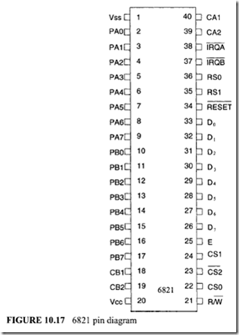
The Motorola 6821 is a 40-pin peripheral interface adapter (PIA) chip. It is provided with an 8-bit bidirectional data bus (D0-D7), two register select lines (RSO, RS 1), read/write (R/W) and reset (RESET) lines, an enable line (E), two 8-bit I/O ports (PAO-PA 7), and (PBO-PB7), and other pins. Figure 10.17 shows the pin diagram of the 6821. There are six 6821 registers. These include two 8-bit ports (ports A and B), two data direction registers, and two control registers. Selection of these registers is controlled by the RSO and RS 1 inputs together with bit 2 of the control register. Table 10.15 shows how the registers are selected. In Table I 0.15, bit 2 in each control register (CRA-2 and CRB-2) determines selection of either an I/O port or the corresponding data direction register when the proper register select signals are applied to RSO and RS 1. A 1 in bit 2 in CRA or CRB allows access of I/O ports; a 0 in bit 2 of CRA or CRB selects the data direction registers.
Each I/O port bit can be configured to act as an input or output. This is accomplished by sending a 1 in the corresponding data direction register bit for those bits that are to be output and a 0 for those bits that are to be inputs. A LOW on the RESET pin clears all PIA registers to 0. This has the effect of configuring PAO-PA 7 and PBO-PB7 as inputs.
Three built- in signals in the 68000 provide the interface with the 6821: enable (E), valid memory address (VMA), and valid peripheral address (VPA). The enable signal (E) is an output from the 68000. It corresponds to theE signal of the 6821. This signal is the clock used by the 6821 to synchronize data transfer. The frequency of the E signal is one tenth of the 68000 clock frequency. This allows one to interface the 68000 (which operates much faster than the 6821) with the 6821. The valid memory address (VMA) signal is output by the 68000 to indicate to the 6800 peripherals that there is a valid address on the address bus. The valid peripheral address (VPA) is an input to the 68000. This signal is used to indicate that the device addressed by the 68000 is a 6800 peripheral. This tells the 68000 to synchronize data transfer with the enable signal (E).
Let us now discuss how the 68000 instructions can be used to configure the 6821 ports. As an example, bit 7 and bits 0-6 of port A can be configured, respectively, as input and outputs using the following instruction sequence:
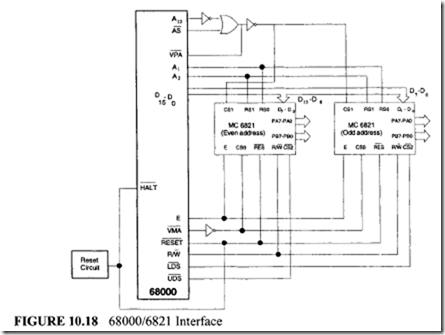
Figure 10.18 shows a block diagram of how two 6821 ‘s are interfaced to the 68000 in order to obtain four 8-bit I/O ports. Note that the least significant bit, A0, of the 68000 address pin is internally encoded to generate two signals, the upper data strobe (UDS) and lower data strobe (LDS). For byte transfers, UDS is asserted if an even-numbered byte is being transferred and LDS is asserted for an odd-numbered byte. In Figure I 0.18, I/O port addresses can be obtained as follows: When A22 = 1 and AS = 0, the OR gate output will be LOW. This OR gate output is used to assert VPA. The inverted OR gate output, in tum, makes CSI HIGH on both 6821 ‘s. Note that A22 is arbitrarily chosen. A22 is chosen to be HIGH to enable CSl so that the addresses for the ports and the reset vector are not the same. Assuming that the D0n’t care address lines A23 and A21-A3 are O’s, the addresses for the I/O ports, control registers, and data direction registers for the even 6821 (A0 = 0) can be obtained as shown; similarly, the addresses for the ports, control registers, and data direction registers for the odd 6821 (A0 = 1) can be determined as follows:
68000/68230 Interface
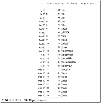
The 68230 is a 48-pin I/O chip designed for the 68000 family of microprocessors. The 68230 offers various functions such as programmed I/O, an on-chip timer, and a DMA request pin for connection to a DMA ‘Controller. Figure I 0.19 shows the 68230 pin diagram. The 68230 can be configured in two modes of operation: unidirectional and bidirectional. In the unidirectional mode, data direction registers configure the corresponding ports as inputs or. outputs. This is the programmed I/O mode of operation. Both 8-bit and 16-bit ports can be used. In the bidirectional mode, the 68230 provides data transfer between the 68000 and external devices via exchange of control signals (known as handshaking). This section will only cover the programmed I/O feature of the 68230.
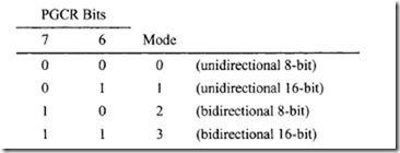
This 68230 ports can be configured in either unidirectional or bidirectional mode by using bits 7 and 6 of the port general control register, PGCR (RO) as follows:
The other bits of the PGCR are defined for handshaking.
Modes 0 and 2 configure ports A and B as unidirectional or bidirectional 8-bit ports. Modes 1 and 3, on the other hand, combine ports A and B together to form a 16-
bit unidirectional or bidirectional port. Ports configured as unidirectional 8-bit must be programmed further as submodes of operation using bits 7 and 6 of PACR (R6) and PBCR (R7) as follows:
Note that X means D0n’t care. Nonlatched inputs are latched internally, but the values are not latched externally by the 68230 at the port. Bit I/O is used for programmed I/O.
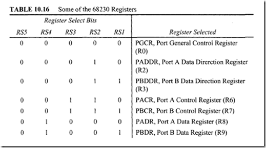
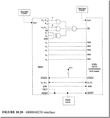
The submodes define the ports as parallel input ports, parallel output ports, or bit-configurable I/O ports. In addition to these, the submodes further define the ports as latched input ports, interrupt-driven ports, DMA ports, and ports with various I/O handshake operations. Table 10.16lists some of the 68230 registers. The registers required for programmed I/O are considered in the following discussion. Note that the 68230 register select pins (RS5-RS I) are used to select the 68230 registers. Figure I 0.20 illustrates how to obtain specific addresses for the 68230 I/O ports.
The hardware schematic for the 68000/68230 interface shown in Figure I 0.20 is connected in such a way that each 68230 I/O port has a unique address. A23 is chosen to be HIGH to select the 68230 chips so that the port addresses are different from the 68000 reset vector addresses 000000 16-000006 16• The configuration in the figure will provide even port addresses because UDS is used for enabling the 68230 CS. The 68230 DTACK is an open drain output. Hence, a pull-up resistor is required.
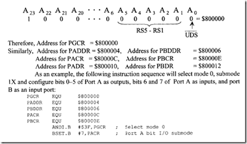
From the figure, addresses for registers PGCR (RO), PADDR (R2), PBDDR (R3), PACR (R6), PBCR (R7), PADR (R8), and PBDR (R9) can be obtained. Consider PGCR as follows:
Example 10.16
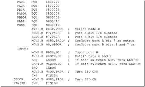
A 68000/68230-based microcomputer is required to drive an LED connected at bit 7 of port A based on two switch inputs connected at bits 6 and 7 of port B. If both switches are equal (either HIGH or LOW), turn the LED ON; otherwise turn it OFF. Assume that a HIGH will turn the LED ON and a LOW will turn it OFF. Write a 68000 assembly program to accomplish this.
Solution
Example 10.17
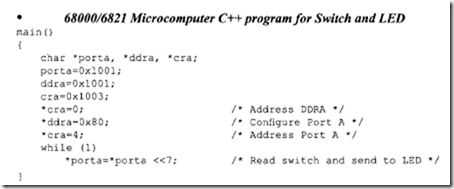
Write a 68000 assembly language program to drive an LED connected to bit 7 of Port A based on a switch input at bit 0 of Port A. If the switch is HIGH, turn the LED ON; otherwise turn the LED OFF. Assume a 68000/2732/6116/6821 microcomputer. Also, write a C++ program to accomplish the same task. Use port addresses of your choice. Solution
The 68000 assembly language program and the C++ program follow.
The C++ compiler will generate more machine codes for the above program compared to the equivalent assembly program. Note that the C++ program is not 100% portable while using I/O. However, it is easier to write programs using C++ than using assembly language.
10.12.2 68000 Interrupt System
The 68000 interrupt I/O can be divided into two types: external interrupts and internal interrupts.
External Interrupts
The 68000 provides seven levels of external interrupts, 1 through 7. The external hardware provides an interrupt level using the pins IPL0 , IPLl, and IPL2. Like other microprocessors, the 68000 checks for and accepts interrupts only between instructions. It compares the value of inverted IPLO-IPL2 with the current interrupt mask contained in the bits 10, 9, and 8 of the status register.
If the value of the inverted IPLO-IPL2 is greater than the value of the current interrupt mask, then the 68000 acknowledges the interrupt and initiates interrupt processing. Otherwise, the 68000 continues with the current interrupt. Interrupt request level 0 (IPLO IPL2 all HIGH) indicates that no interrupt service is requested. An inverted IPL2, IPLl, IPLO of 7 is always acknowledged. Therefore, interrupt level 7 is "nonmaskable." Note that the interrupt level is indicated by the interrupt mask bits (inverted IPL2, IPL1 , IPLO).
To ensure that an interrupt will be recognized, the following interrupting rules should be considered:
1. The incoming interrupt request level must have a higher priority level than the mask level set in the interrupt mask bits (except for level 7, which is always recognized).
2. The IPL2-IPLO pins must be held at the interrupt request level until the 68000 acknowledges the interrupt by initiating an interrupt acknowledge (lACK) bus cycle
Interrupt level 7 is edge-triggered. On the other hand, interrupt levels 1–6 are level sensitive. However, as s00n as one of them is acknowledged, the processor updates its interrupt mask at the same level.
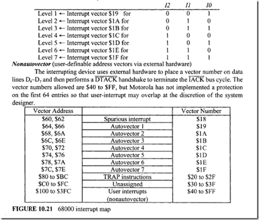
The 68000 D0es not have any EI (enable interrupt) or DI (disable interrupt) instructions. Instead, the level indicated by 12 11 10 in the SR disables all interrupts below or equal to this value and enables all interrupts above. For example, ifl211 IO = 100, then interrupt levels 1–4 are disabled and 5-7 are enabled. Note that 12 11 IO = 000 enables all interrupts and I211 IO = 111 disables all interrupts except level 7 (nonmaskable).
Once the 68000 has decided to acknowledge an interrupt, it performs several steps:
1. Makes an internal copy of the current status register.
2. Updates the priority mask and address lines A3-A1 with the level of the interrupt recognized (inverted IPL pins) and then asserts AS to inform the external devices that A 1-A3 has the interrupt level.
3. Enters the supervisor state by setting the S bit in SR to 1.
4. Clears the T bit in SR to inhibit tracing.
5. Pushes the program counter (PC) onto the supervisor stack.
6. Pushes the internal copy of the old SR onto the supervisor stack.
7. Runs an lACK bus cycle for vector number acquisition (to provide the address of the service routine).
8. Multiplies the 8-bit interrupt vector by 4. This points to the location that contains the starting address of the interrupt service routine.
9. Jumps to the interrupt service routine.
10. The last instruction of the service routine should be RTE, which restores the original status word and program counter by popping them from the supervisor stack.
External logic can respond to the interrupt acknowledge in one of three ways: byrequesting automatic vectoring (autovector), by placing a vector number on the data bus (nonautovector), or by indicating that no device is responding (spurious interrupt). Autovector (address vectors predefined by Motorola)
If the hardware asserts VPA to terminate the JACK bus cycle, the 68000 directs itself automatically to the proper interrupt vector corresponding to the current interrupt level. No external hardware is inquired for providing the interrupt address vector. The seven levels of autovector interrupt are listed below:
Another way to terminate an interrupt acknowledge bus cycle is with the BERR (bus error) signal. Even though the interrupt control pins are synchronized to enhance noise immunity, it is possible that external system interrupt circuitry may initiate an lACK bus cycle as a result of noise. Because no device is requesting interrupt service, neither DTACK nor VPA will be asserted to signal the end of the nonexisting lACK bus cycle. When there is no response to an lACK bus cycle after a specified period of time (monitored by the user using an external timer), BERR can be asserted by an external timer. This indicates to the processor that it has recognized a spurious interrupt. The 68000 provides ISH as the vector to fetch for the starting address of this exception-hanD1ing routine.
It should be pointed out that the spurious interrupt and bus error interrupt due to a troubled instruction cycle (when no DTACK is received by the 68000) have two different interrupt vectors. Spurious interrupt occurs when the BERR pin is asserted during interrupt processing.
Internal Interrupts
The internal interrupt is a software interrupt. This interrupt is generated when the 68000 executes a software interrupt instruction (TRAP) or by some undesirable events such as division by zero or execution of an illegal instruction.
68000 Interrupt Map
The 68000 uses an 8-bit vector n to obtain the interrupt address vector. The 68000 reads the long-word located at memory 4* n. This long word is the starting address of the service routine. Figure 10.21 shows an interrupt map of the 68000. Vector addresses $00 through $2E (not shown in the figure) include vector addresses for reset, bus error, trace, divide by 0, and so on, and addresses $30 through $5C are unassigned. The RESET vector requires four words (addresses 0, 2, 4, and 6); the other vectors require only two words.
After hardware reset, the 68000 loads the supervisor SP high and low words, respectively, from addresses 000000 16 and 000002 16, and the PC high and low words, respectively, from 000004 16 and 000006 16• The typical assembler directive DC (define constant) can be used to load the PC and Supervisor SP. For example, the following will load A7′ with $16F128 and PC with $781624:
 68000 Interrupt Address Vector
Suppose that the user decides to write a service routine starting at location $123456 using autovector 1. Because the autovector 1 address is $000064 and $000066, the numbers $0012 and $3456 must be stored in locations $000064 and $000066, respectively. Note that from Figure 10.21, n = $19 for autovector I. Hence, the starting address of the service routine is obtained from the contents of the address 4 x $19 = $000064.
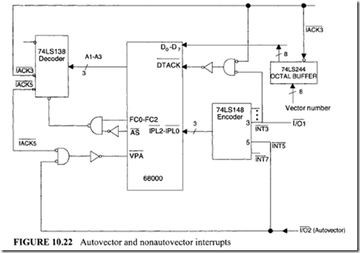
An Example of Autovector and Nonautovector Interrupts
As an example to illustrate the concept of autovector and nonautovector interrupts, consider Figure I 0.22. In this figure, I/O device I uses nonautovector and I/O device 2 uses autovector interrupts. The system is capable of hanD1ing interrupts from seven devices (IPL2 IPLI IPLO pins= 111 means no interrupt) because an 8-to-3 priority encoder such as the 74LS148 is used. The 74LS148 provides an inverted three-bit output with input 7 as the highest priority and input 0 as the lowest priority. Hence, if all eight inputs of the 74LSI48 are low simultaneously, the three-bit output will be 000 (inverted 111) indicating a LOW
on input 7. In figure 10.22, I/O1 and I/O2 from the interrupting devices are connected to inputs 3 and 5 ofthe 74LSI48 encoder respectively. This means that the device with I/O2 as the interrupting signal will generate level 5 autovectored interrupt while the device with I/O 1 as the interrupting signal will generate the nonautovectored interrupt.
Suppose that I/O device 2 drives I/O2 LOW in order to activate line 5 of the 74LS148. This, in tum, will generate a LOW on input 5 of the 74LS148. This will provide 010 (inverted I 01) on IPL2 IPLI IPLO pins of the 68000 generating a level 5 autovectored interrupt. When the 68000 decides to acknowledge the interrupt, it drives FCO-FC2 HIGH. The interrupt level is reflected on A 1-A3 when AS is activated by the 68000. The IACK5 and I/O2 signals are used to generate VPA. Once VPA is asserted, the 68000 obtains the interrupt vector address using autovectoring.
In the case of I/O1, line 3 of the priority encoder is activated to initiate the nonautovectored interrupt. By using appropriate logic, DTACK is asserted using IACK3 and I/O1. The vector number is placed on D0-D7 by enabling an octal buffer such as the 74LS244 using IACK3. The 68000 inputs this vector number and multiplies it by 4 to obtain the interrupt address vector.
Interfacing a Typical AID Converter to the 68000 Using Autovector and Nonautovector Interrupts
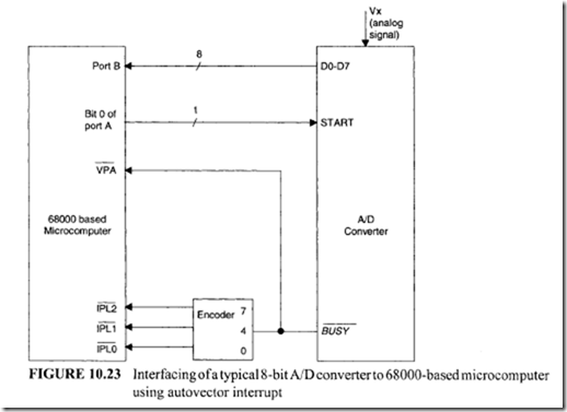
Figure 10.23 shows the interfacing of a typical A/D converter to the 68000-based microcomputer using the autovector interrupt. In the figure, the AJD converter can be started by sending a START pulse. The signal can be connected to line 4 (for example) of the encoder.
Note that line 4 is 1002 for IPL2, IPLl, IPLO, which is a level 3 (inverted 1002) interrupt. BUSY can be used to assert VPA so that, after acknowledgment of the interrupt, the 68000 will service the interrupt as a level 3 autovector interrupt. Note that the encoder in Figure I 0.23 is used for illustrative purposes. This encoder is not required for a single device such as the A/D converter in the example.
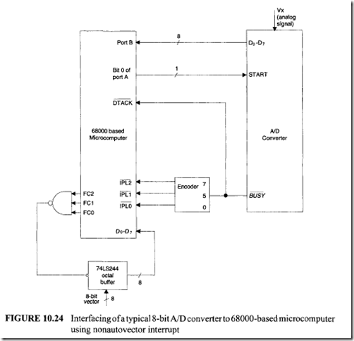
Figure 10.24 shows the interfacing of a typical A/D converter to the 68000-based microcomputer using the nonautovector interrupt. In the figure, the 68000 starts the A/D converter as before. Also, the BUSY signal is used to interrupt the microcomputer using
line 5 (IPL2, IPTI, lPLO= 101, which is a level2 interrupt) of the encoder. BUSY can be used to assert DTACK so that, after acknowledgment of the interrupt, FC2, FC I, FCO will become 1112, which can be NANDed to enable an octal buffer such as the 74LS244 in order to transfer an 8-bit vector from the input of the buffer to the D0-D7 lines of the 68000. The 68000 can then multiply this vector by 4 to determine the interrupt address vector. As before, the encoder in Figure I 0.24 is not required for the single AJD converter.
10.12.3 68000 DMA
Three DMA control lines are provided with the 68000. These are BR (bus request), BG (bus grant}, and BGACK (bus grant acknowledge). The BR line is an input to the 68000. The external device activates this line to tell the 68000 to release the system bus. At least one clock period after receiving BR, the 68000 will enable its BG output line to acknowledge the DMA request. However, the 68000 will not relinquish the bus until it has completed the current instruction cycle. The external device must check the AS (address strobe) line to determine the completion of the instruction cycle by the 68000. When AS becomes HIGH, the 68000 will tristate its address and data lines and will give up the bus to the external device. After taking over the bus, the external device must enable the BGACK line. The BGACK line tells the 68000 and other devices connected to the bus that the bus is being used. The 68000 stays in a tristate condition until BGACK becomes HIGH.
