10.13 68000 Exception Handlin :
A 16-bit microcomputer is usually capable of hanD1ing unusual or exceptional conditions. These conditions include situations such as execution of illegal instruction or division by zero. In this section, the exception-hanD1ing capabilities of the 68000 are described.
The 68000 exceptions can be divided into three groups, namely, groups 0, 1, and 2. Group 0 has the highest priority, and group 2 has the lowest priority. Within each group, there are additional priority levels. A list of 68000 exceptions along with individual priorities is as follows:
Group 0 Reset (highest level in this group}, address error (next level), and bus error (lowest level)
Group 1 Trace (highest level), interrupt (next level), illegal op-code (next level), and privilege violation (lowest level)
Group 2 TRAP, TRAPV, CHK, and ZERO DIVIDE (no individual priorities assigned in group 2)
Exceptions from group 0 always override an active exception from group 1 or group 2.
Group 0 exception processing begins at the completion of the current bus cycle (2 clock cycles). Note that the number of cycles required for a READ or WRITE operation is called a "bus cycle." This means that during an instruction fetch if there is a group 0 interrupt, the 68000 will complete the instruction fetch and then service the interrupt. Group I exception processing begins at the completion of the current instruction. Group 2 exceptions are initiated through execution of an instruction. Therefore, there are no individual priority levels within group 2. Exception processing occurs when a group 2 interrupt is encountered, provided there are no group 0 or group 1 interrupts.
When an exception occurs, the 68000 saves the contents of the program counter
and status register onto the stack and then executes a new program whose address is provided by the exception vectors. Once this program is executed, the 68000 returns to the main program using the stored values of program counter and status register.
Exceptions can be of two types: internal or external. The internal exceptions are generated by situations such as division by zero, execution of illegal or unimplemented instructions, and address error. As mentioned before, internal interrupts are called "traps." The external exceptions are generated by bus error, reset, or interrupt instructions. The basic concepts associated with interrupts, relating them to the 68000, have already been described. In this section, we will discuss the other exceptions.
In response to an exceptional condition, the processor executes a user-written program. In some microcomputers, one common program is provided for all exceptions. The beginning section of the program determines the cause of the exception and then branches to the appropriate routine. The 68000 utilizes a more general approach. Each exception can be hanD1ed by a separate program.
As mentioned before, the 68000 has two modes of operation: user state and supervisor state. The operating system runs in supervisor mode, and all other programs are executed in user mode. The supervisor state is therefore more privileged. Several privileged instructions such as MOVE to SR can be executed only in supervisor mode. Any attempt to execute them in user mode causes a trap.
We will now discuss how the 68000 hanD1es exceptions caused by external resets, trap instructions, bus and address errors, tracing , execution of privileged instructions in user mode, and execution of illegal/unimplemented instructions:
-
The reset exception is generated externally. In response to this exception, the 68000 automatically loads the initial starting address into the processor.
-
The 68000 has a TRAP instruction, which always causes an exception. The operand for this instruction varies from 0 to 15. This means that there are 16 TRAP instructions. Each TRAP instruction has an exception vector. TRAP instructions are normally used to call subroutines in an operating system. Note that this automatically places the 68000 in supervisor state. TRAPs can also be used for inserting breakpoints in a program. Two other 68000 instructions cause traps if a particular condition is true: TRAPV and CHK. TRAPV generates an exception if the overflow flag is set. The TRAPV instruction can be inserted after every arithmetic operation in a program in order to cause a trap whenever there is the possibility of an overflow. A routine can be written at the vector address for the TRAPV to indicate to the user that an overflow has occurred. The CHK instruction is designed to ensure that access to an array in memory is within the range specified by the user. If there is a violation ofthis range, the 68000 generates an exception.
-
A bus error occurs when the 68000 tries to access an address that D0es not belong to the devices connected to the bus. This error can be detected by asserting the BERR pin on the 68000 chip by an external timer when no DTACK is received from the device after a certain period of time. In response to this, the 68000 executes a user-written routine located at an address obtained from the exception vectors. An address error, on the other hand, occurs when the 68000 tries to read or write a word (16 bits) or long word (32 bits) in an odd address. This address error has a different exception vector from the bus error.
-
The trace exception in the 68000 can be generated by setting the trace bit in the status register. In response to the trace exception, the 68000 causes an internal exception after execution of every instruction. The user can write a routine at the exception vectors for the trace instruction to display register and memory contents. The trace exception provides the 68000 with the single-stepping
-
As mentioned before, the 68000 has privileged instructions, which must be executed in supervisor mode. An attempt to execute these instructions causes privilege violation.
-
Finally, the 68000 causes an exception when it tries to execute an illegal or unimplemented instruction.
10.14 68000/2732/6116/6821-Based Microcomputer
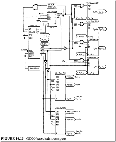
Figure I 0.25 shows the schematic of a 68000-based microcomputer with a 4K EPROM, a 4K static RAM, and four 8-bit I/O ports. Let us explain the various sections of the hardware schematic. Two 2732 and two 6116 chips are required to obtain the 4K EPROM and 4K RAM. The LDS and UDS pins are ORed with the memory select signal to enable the chip selects for the EPROMs and the RAMs. Address decoding is accomplished by using a 3 x 8 decoder. The decoder enables the memory or the I/O chips depending on the status of address lines A 12-A14 and the AS line of the 68000. AS is used to enable the decoder. I;; selects the EPROMs, I;" selects the RAMs, and I; selects the I/O ports.
When addressing memory chips, the DTACK input of the 68000 must be asserted for data acknowledge. The 68000 clock in the hardware schematic is 10 MHz. Therefore, each clock cycle is I 00 ns. In Figure I 0.25, AS is used to enable the 3 x 8 decoder. The outputs of the decoder are gated to assert 68000 DTACK. This means that AS is indirectly
used to assert DTACK. From the 68000 read timing diagram, AS goes to LOW after approximately 2 cycles (200 ns for the 10-MHz clock) from the beginning of the bus cycle. With no wait states, the 68000 samples DTACK at the falling edge of S4 (300 ns) and, if DTACK is recognized, the 68000 latches data at the falling edge of S6 (400 ns). If DTACK is not recognized at the falling edge of S4, the 68000 inserts a !-cycle (I 00 ns in this case) wait state, samples DTACK at the end of S6, and, if DTACK is recognized, latches data at the end ofS8 (500 ns), and the process continues. Because the access time of the 2732 is 200 ns (Used to be 450ns), data will not be available at the output pins of the 2732’s until after approximately 400 ns. To be on the safe side, DTACK recognition by the 68000 at the falling edge of S6 (400 ns) and latching of data at the falling edge of S8 (500 ns) will definitely satisfy the timing requirement. This means that the decoder output fo for EPROM select should go to LOW at the end of S6. Therefore, 200ns delay (Two cycles) for DTACK is assumed.
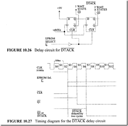
A delay circuit, as shown in Figure I 0.26, is designed using two D flip-flops.
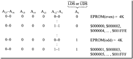
EPPOM select activates the delay circuit. The input is then shifted right 2 bits to obtain a 2- cycle wait state to allow sufficient time for data transfer. DTACK assertion and recognition are delayed by 2 cycles during data transfer with EPROMs. Figure 10.27 shows the timing diagram for the DTACK delay circuit. Note that DTACK goes to Low after about 2 cycles if asserted by AS providing erronous result. Therefore, DTACK must be delayed.
When the EPROM is not selected by the decoder, the clear pin is asserted (output of inverter), so Q is forced LOW and Q is HIGH. Therefore, DTACK is not asserted. When the processor selects the EPROMs, the output of the inverter is HIGH, so the clear pin is not asserted. The D flip-flop will accept a high at the input, and Q2 will be HIGH and Q2 will be LOW. Now that Q2 is LOW, it can assert DTACK. Ql will provide one wait cycle and Q2 will provide two wait cycles. Because the 2732 EPROM has a 200-ns access time and the microprocessor is operating at 10 MHz (I00-ns clock cycle), two wait cycles are inserted before asserting DTACK (2 x 100 = 200 ns). Therefore, Q2 can be connected to the DTACK pin through an AND gate. No wait state is required for RAMs because the access time for the RAMs is only 120 nanoseconds.
Four 8-bit I/O ports are obtained by using two 6821 chips. When the I/O ports are selected, the VPA pin is asserted instead of DTACK. This will acknowledge to the 68000 that it is addressing a 6800-type peripheral. In response, the 68000 will synchronize all data transfer with the E clock.
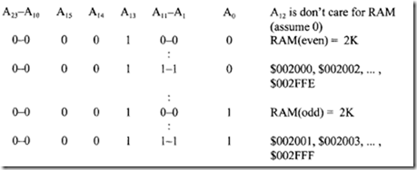
The memory and I/O maps for the schematic are as follows:
-
Memory Maps (all numbers in hex). A23 – A 16 are D0n’t cares and assumed to be 0’s .
Note that, upon hardware reset, the 68000 loads the supervisor SP high and low words, respectively, from addresses $000000 and $000002 and the PC high and low words, respectively, from locations $000004 and $000006. The memory map contains these reset vector addresses in the even and odd 2732 chips.
-
Memory Mapped I/O (all numbers in hex). A23-A16 and A 12-A3 are D0n’t cares and assumed to be 0’s.
For both memory and I/O chips, AS, UDS and LDS must be used in chip select logic. Note that:
1. For memory, both even and odd chips are required. However, for I/O chips, an odd-addressed I/O chip, an even-addressed I/O chip, or both can be used, depending on the number of ports required in an application. UDS and/or LDS must be used in I/O chip select logic depending on the number of IIO chips used. The same chip select logic must be used for both the even and its corresponding odd memory chip.
2. DTACK must be connected to an external input (typically a signal from the address decoding logic) to satisfy the timing requirements. In many instances, AS is directly connected to DTACK.
3. The 68000 must be connected to ROMs I EPROMs I PPROMs in such a way that the 68000 RESET vector address is included as part of the memory map.
10.15 Multiprocessine with the 68000 Using theTAS Instruction and the AS Sienal
![]() Earlier, the 68000 TAS instruction was discussed. The TAS instruction supports the software aspects of interfacing two or more 68000’s via shared RAM. When TAS is executed, the 68000 AS pin stays low. During both the read and write portions of the cycle, AS remains LOW and the cycle starts as the normal read cycle. However, in the normal read, AS going inactive indicates the end of the read. During execution of TAS, AS stays LOW throughout the cycle, so AS can be used in the design as a bus-locking circuit. Due to the bus locking, only one processor at a time can perform a TAS operation in a multiprocessor system.The TAS instruction supports multiprocessor operations (globally shared resources) by checking a resource for availability and reserving or locking it for use by a single processor.
Earlier, the 68000 TAS instruction was discussed. The TAS instruction supports the software aspects of interfacing two or more 68000’s via shared RAM. When TAS is executed, the 68000 AS pin stays low. During both the read and write portions of the cycle, AS remains LOW and the cycle starts as the normal read cycle. However, in the normal read, AS going inactive indicates the end of the read. During execution of TAS, AS stays LOW throughout the cycle, so AS can be used in the design as a bus-locking circuit. Due to the bus locking, only one processor at a time can perform a TAS operation in a multiprocessor system.The TAS instruction supports multiprocessor operations (globally shared resources) by checking a resource for availability and reserving or locking it for use by a single processor.
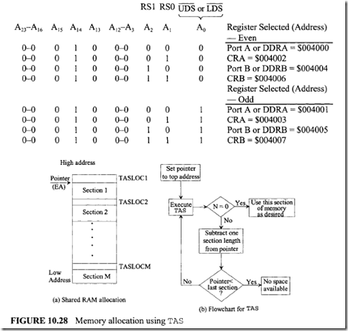
The TAS instruction can, therefore, be used to allocate free memory spaces . The TAS instruction execution flowchart for allocating memory is shown in Figure 10.28. The shared RAM of the Figure 10.28 is divided into M sections. The first byte of each section will be pointed to by (EA) of theTAS (EA) instruction. In the flowchart of Figure 10.28, (EA) first points to the first byte of section 1. The instruction TAS (EA) is the executed. The TAS instruction checks the most significant bit (N bit) in (EA). N = 0 indicates that section 1 is free; N = 1 means that section 1 is busy. If N = 0, then section 1 will be allocated for use. If N = 1 (section 1 is busy), then a program will be written to subtract one section length from (EA) to check the next section for availability. Also, (EA) must be checked with the value TASLOCM. If (EA) < TASLOCM, then no space is available for allocation. However, if (EA) > TASLOCM, then TAS is executed and the availability of that section is determined.
![]() In a multiprocessor environment, the TAS instruction provides software support for interfacing two or more 68000’s via shared RAM. The AS signal can be used to provide the bus-locking mechanism.
In a multiprocessor environment, the TAS instruction provides software support for interfacing two or more 68000’s via shared RAM. The AS signal can be used to provide the bus-locking mechanism.
Example 10.18
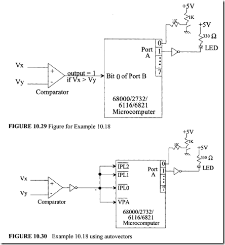
Assume that the 68000127321611616821 microcomputer shown in Figure 10.29 is required to perform the following:
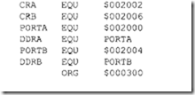
(a) If Vx > Vy , tum the LED ON if the switch is open; otherwise tum the LED OFF. Write a 68000 assembly language program starting at address $000300 to accomplish the above by inputting the comparator output via bit 0 of Port B. Use Port A address= $002000, Port B address = $002004, CRA = $002002, CRB = $002006. Assume the
LED is OFF initially.
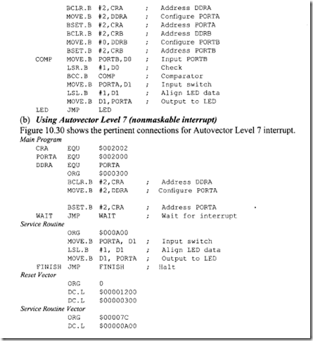
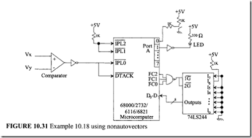
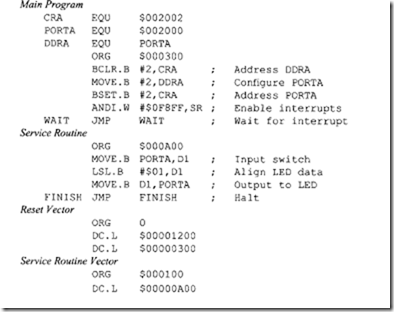
(b) Repeat part (a) using autovector level 7 and nonautovector (Vector $40). Use Port A (address $002000) for LED and switch as above with CRA=$002002. Assume supervisor mode. Write the main program and service routine in 68000 assembly language starting at addresses $000300 and $000A00 respectively. Also, initialize the supervisor stack pointer at $001200.
Solution
(a) Using Programmed I/O
From figure 10.29, the following 68000 assembly language program can be written:
Using Nonautovectoring (vector $40)
Figure 10.31 shows the pertinent connections for nonautovectoring interrupt.
