8.2.3 Direct Memory Access (DMA)
Direct memory access (DMA) is a technique that transfers data between a microcomputer’s memory and an I/O device without involving the microprocessor. DMA is widely used in transferring large blocks of data between a peripheral device such as a hard disk and the microcomputer’s memory. The DMA technique uses a DMA controller chip for the data transfer operations. The DMA controller chip implements various components such as a counter containing the length of data to be transferred in hardware in order to speed up data transfer. The main functions of a typical DMA controller are summarized as follows:
-
The I/O devices request DMA operation via the DMA request line of the controller chip. The controller chip activates the microprocessor HOLD pin, requesting the microprocessor to release the bus.
-
The processor sends HLDA (hold acknowledge) back to the DMA controller, indicating that the bus is disabled. The DMA controller places the current value of its internal registers, such as the address register and counter, on the system bus and sends a DMA acknowledge to the peripheral device. The DMA controller completes the DMA transfer.
There are three basic types of DMA: block transfer, cycle stealing, and interleaved DMA. For block-transfer DMA, the DMA controller chip takes over the bus from the microcomputer to transfer data between the microcomputer memory and I/O device. The microprocessor has no access to the bus until the transfer is completed. During this time, the microprocessor can perform internal operations that do not need the bus. This method is popular with microprocessors. Using this technique, blocks of data can be transferred.
Data transfer between the microcomputer memory and an I/O device occurs on a word-by-word basis with cycle stealing. Typically, the microprocessor is generated by ANDing an INHIBIT signal with the system clock. The system clock has the same frequency as the microprocessor clock. The DMA controller controls the INHIBIT line. During normal operation, the INHIBIT line is HIGH, providing the microprocessor clock. When DMA operation is desired, the controller makes the INHIBIT line LOW for one clock cycle. The microprocessor is then stopped completely for one cycle. Data transfer
between the memory and I/O takes place during this cycle. This method is called "cycle stealing" because the DMA controller takes away or steals a cycle without microprocessor recognition. Data transfer takes place over a period of time.
With interleaved DMA, the DMA controller chip takes over the system bus when the microprocessor is not using it. For example, the microprocessor does not use the bus while incrementing the program counter or performing an ALU operation. The DMA controller chip identifies these cycles and allows transfer of data between the memory and I/O device. Data transfer takes place over a period of time for this method.
Because block-transfer DMA is common with microprocessors, a detailed
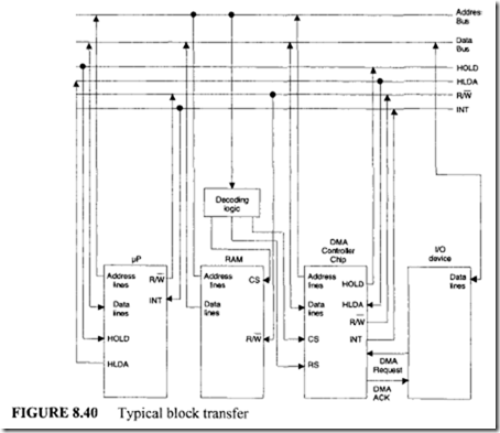
description is provided. Figure 8.40 shows a typical diagram of the block-transfer DMA. In the figure, the I/O device requests the DMA transfer via the DMA request line connected to the controller chip. The DMA controller chip then sends a HOLD signal to the microprocessor, and it then waits for the HOLD acknowledge (HLDA) signal from the microprocessor. On receipt of the HLDA, the controller chip sends a DMA ACK signal to the I/O device. The controller takes over the bus and controls data transfer between the RAM and I/O device. On completion of the data transfer, the controller interrupts the microprocessor by the INT line and returns the bus to the microprocessor by disabling the HOLD and DMA ACK signals.
The DMA controller chip usually has at least three registers normally selected
by the controller’s register select (RS) line: an address register, a terminal count register, and a status register. Both the address and terminal counter registers are initialized by the microprocessor. The address register contains the starting address of the data to be transferred, and the terminal counter register contains the desired block to be transferred. The status register contains information such as completion ofDMA transfer. Note that the
 DMA controller implements logic associated with data transfer in hardware to speed up the DMA operation.
8.3 Summary of I/O
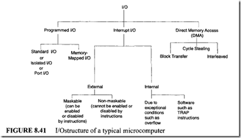
Figure 8.41 summarizes various 110 devices associated with a typical microprocessor.
8.4 Fundamentals of Parallel Processin :
The term "parallel processing" means improving the performance of a computer system by carrying out several tasks simultaneously. A high volume of computation is often required in many application areas, including real-time signal processing. A conventional single computer contains three functional elements: CPU, memory, and I/O. In such a uniprocessor system, a reasonable degree of parallelism was achieved in the following manner:
l. The IBM 370/168 and CDC 6600 computers included a dedicated I/O processor.
This additional unit was capable of performing all I/O operations by employing the DMA technique discussed earlier. In these systems, parallelism was achieved by keeping the CPU and I/O processor busy as much as possible with program execution and I/O operations respectively.
2. In the CDC 6600 CPU, there were 24 registers and 10 execution units. Each execution unit was designed for a specific operation such as addition, multiplication, and shifting. Since all units were independent of each other, several operations were performed simultaneously.
3. In many uniprocessor systems such as IBM 360, parallelism was achieved by using high-speed hardware elements such as carry-look-ahead adders and carry-save adders.
4. In several conventional computers, parallelism is incorporated at the instruction execution level. Recall that an instruction cycle typically includes activities such as op code fetch, instruction decode, operand fetch, operand execution, and result saving. All these operations can be carried out by overlapping the instruction fetch phase with the instruction execution phase. This is known as instruction pipelining. This pipelining concept is implemented in the state-of-the-art microprocessors such as Intel’s Pentium series.
5. In many uniprocessor systems, high throughput is achieved by employing high speed memories such as cache and associative memories. The use of virtual memory concepts such as paging and segmentation also allows one to achieve high processing rates because they reduce speed imbalance between a fast CPU and a slow periphal device such as a hard disk. These concepts are also implemented in today’s microprocessors to achieve high performance.
6. It is a common practice to achieve parallelism by employing software methods such as multiprogramming and time sharing in uniprocessors. In both techniques, the CPU is multiplexed among several jobs. This results in concurrent processing, which improves the overall system throughput.
8.4.1 General Classifications of Computer Architectures
Over the last two decades, parallel processing has drawn the attention of many research workers, and several high-speed architectures have been proposed. To present these results in a concise manner, different architectures must be classified in well defined groups.
All computers may be categorized into different groups using one of three classification methods:
1. Flynn
2.Feng
3. Handler
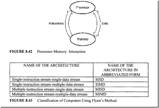
The two principal elements of a computer are the processor and the memory. A processor manipulates data stored in the memory as dictated by the instruction. Instructions are stored in the memory unit and always flow from memory to processor. Data movement
is bidirectional, meaning data may be read from or written into the memory. Figure 8.42 shows the processor-memory interaction.
The number of instructions read and data items manipulated simultaneously by the processor form the basis for Flynn’s classification. Figure 8.43 shows the four types of computer architectures that are defined using Flynn’s method. The SISD computers are capable of manipulating a single data item by executing one instruction at a time. The SISD classification covers the conventional uniprocessor systems such as the VAX-11, IBM 370, Intel 8085, and Motorola 6809. The processor unit of a SISD machine may have one or many functional units. For example, the VAX-11/780 is a SISD machine with a single functional unit. CDC 6600 and IBM 370/168 computers are typical examples of SISD systems with multiple functional units. In a SISD machine, instructions are executed in a strictly sequential fashion. The SIMD system allows a single instruction to manipulate several data elements. These machines are also called vector machines or array processors. Examples of this type of computer are the ILLIAC-IV and Burroughs Scientific Processor (BSP).
The ILLIAC- IV was an experimental parallel computer proposed by the University of Illinois and built by the Burroughs Corporation. In this system, there are 64 processing elements. Each processing element has its own small local memory unit. The operation of all the processing elements is under the control of a central control unit (CCU). Typically, the CCU reads an instruction from the common memory and broadcasts the same to all processing units so the processing units can all operate on their own data at the same time. This configuration is very useful for carrying out a high volume of computations that are encountered in application areas such as finite-element analysis, logic simulation, and spectral analysis. Modem microprocessors such as Intel Pentium II use the SIMD architecture.
By definition, MISD refers to a computer in which several instructions manipulate the same data stream concurrently. The notion of pipelining is very close to the MISD definition.
A set of instructions constitute a program, and a program operates on several data elements. MIMD organization refers to a computer that is capable of processing several programs simultaneously. MIMD systems include all multiprocessing systems. Based on the degree of processor interaction, multiprocessor systems may be further divided into two groups: loosely coupled and tightly coupled. A tightly coupled system has high interaction between processors. Multiprocessor systems with low interprocessor communications are referred to as loosely coupled systems.
In Feng’s approach, computers are classified according to the number of bits processed within a unit time. However, Handler’s classification scheme categorizes computers on the basis of the amount of parallelism found at the following levels:
-
CPU
-
ALU
-
Bit
A thorough discussion of these schemes is beyond the scope of this book. Since contemporary microprocessors such as Intel Pentium II use SIMD architechture, a basic coverage of SIMD is provided next. The SIMD computers are also called array processors. A synchronous array processor may be defined as a computer in which a set of identical processing elements act under the control of a master controller (MC). A command given by the MC is simultaneously executed by all processing elements, and a SIMD system is formed. Since all processors execute the same instruction, this organization offers a great
attraction for vector processing applications such as matrix manipulation.
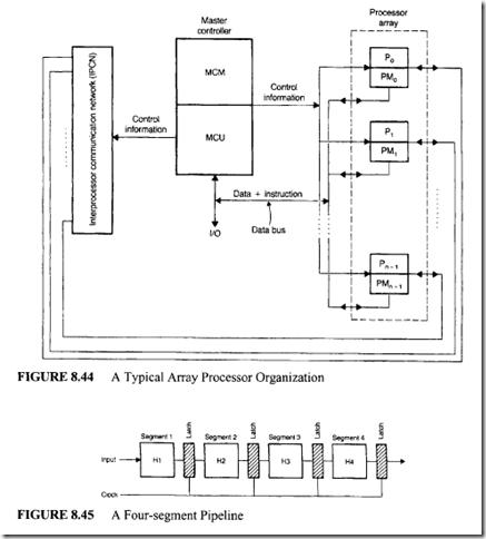
A conceptual organization of a typical array processor is shown in Figure 8.44. The Master Controller (MC) controls the operation of the processor array. This array consists ofN identical processing elements (P0 through Pn- 1). Each processing element P; is assumed to have its own memory, PMi, to store its data. The MC of Figure 8.44 contains two major components:
-
The master control unit (MCU)
-
The master control memory (MCM)
The MCU is the CPU of the master controller and includes an ALU and a set of registers. The purpose of the MCM is to hold the instructions and common data.
Each instruction of a program is executed under the supervision of the MCU in a sequential fashion. The MCU fetches the next instruction, and the execution of this instruction will take place in one of the following ways:
-
If the instruction fetched is a scalar or a branch instruction, it is executed by the MC itself.
-
If the instruction fetched is a vector instruction, such as vector add or vector multiply, then the MCU broadcasts the same instruction to each Pi, of the processor array, allowing all P;’s to execute this instruction simultaneously.
Assume the required data is already within the processing element’s private memory. Before execution of a vector instruction, the system ensures that appropriate data values are routed to each processing element’s private memory. Such an operation can be performed in two ways:
-
All data values can be transferred to the private memories from an external source via the system data bus.
-
The MCU can transfer the data values to the private memories via the control bus.
In an array processor like the one shown in Figure 8.44, it may be necessary to disable some processing elements during a vector operation. This is accomplished by including a mask register, M, in the MCU. The mask register contains a bit, m;, for each processing element, p;. A particular processing element, p;, will respond to a vector instruction broadcast by the MCU only when its mask bit, m;, is set to 1; otherwise, the processing element. P;, will not respond to the vector instruction and is said to be disabled.
In an array processor, it may be necessary to exchange data between processing elements. Such an exchange of data between processing elements takes place through the path provided by the interprocessor communication network (IPCN). Data exchanges refers to exchanges between scratchpad registers of the processing elements and exchanges between private memories of the processing elements.


