6.4 The Memory
The main or external memory (or simply the memory) stores both instructions and data. For 8-bit microprocessors, the memory is divided into a number of 8-bit units called "memory words." An 8-bit unit of data is termed a "byte." Therefore, for an 8-bit microprocessor, "memory word" and "memory byte" mean the same thing. For 16-bit microprocessors, a word contains two bytes (16 bits). A memory word is identified in the memory by an address. For example, the 8086 microprocessor uses 20-bit addresses for accessing
memory words. This provides a maximum of 220 = I MB of memory addresses, ranging rom 0000016 to FFFFF 16 in hexadecimal.
As mentioned before, an important characteristic of a memory is whether it is volatile or nonvolatile. The contents of a volatile memory are lost if the power is turned off. On the other hand, a nonvolatile memory retains its contents after power is switched off. Typical examples of nonvolatile memory are ROM and magnetic memory (floppy disk). A RAM is a volatile memory unless backed up by battery.
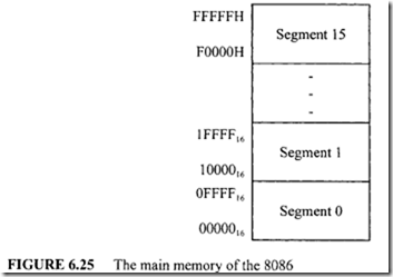
As mentioned earlier, some microprocessors such as the Intel 8086 divide the memory into segments. For example, the 8086 divides the I MB main memory into 16 segments (0 through 15). Each segment contains 64 KB of memory and is addressed by 16 bits. Figure 6.25 shows a typical main memory layout of the 8086. In the figure, the high four bits of an address specify the segment number. As an example, consider address I 0005 16 of segment l. The high four bits, 000 I, of this address define the location is in segment 1 and the low 16 bits, 0005 16, specify the particular address in segment 1. The 68000, on the other hand, uses linear or nonsegmented memory. For example, the 68000 uses 24 address pins to directly address 224 = 16MB of memory with addresses from 000000
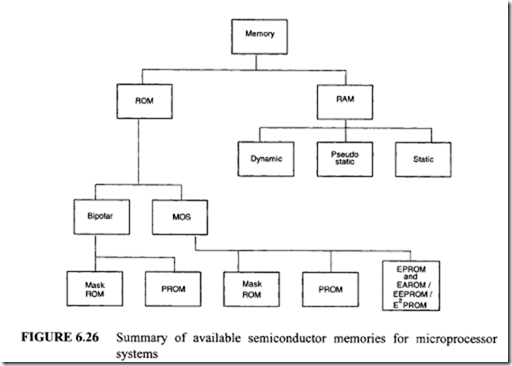
to FFFFFF 16• As mentioned before, memories can be categorized into two main types: read-only memory (ROM) and ranD0m-access memory (RAM). As shown in Figure 6.26, ROMs and RAMs are then divided into a number of subcategories, which are discussed next.
6.4.1 RanD0m-Access Memory (RAM)
There are three types of RAM: dynamic RAM, pseuD0-static RAM , and static RAM. Dynamic RAM stores data in capacitors, that is, it can hold data for a few milliseconds. Hence, dynamic RAMs are refreshed typically by using external refresh circuitry. PseuD0 static RAMs are dynamic RAMs with internal refresh. Finally, static RAM stores data
in flip-flops. Therefore, this memory D0es not need to be refreshed. RAMs are volatile unless backed up by battery. Dynamic RAMs (DRAMs) are used in applications requiring large memory. DRAMs have higher densities than Static RAMs (SRAMs). Typical examples of DRAMs are 4464 (64K x 4-bit), 44256 (256K x 4-bit), and 41000 (1M x 1-bit). DRAMs are inexpensive, occupy less space, and dissipate less power compared to SRAMs. Two enhanced versions of DRAM are ED0 DRAM (Extended Data Output DRAM) and SDRAM (Synchronous DRAM). The ED0 DRAM provides fast access by allowing the DRAM controller to output the next address at the same time the current data is being read. An SDRAM contains multiple DRAMs (typically 4) internally. SDRAMs utilize the multiplexed addressing of conventional DRAMs . That is, SDRAMs provide row and column addresses in two steps like DRAMs. However, the control signals and address inputs are sampled by the SDRAM at the leading edge of a common clock signal ( 133 MHz maximum). SDRAMs provide higher densities by further reducing the need for support circuitry and faster speeds than conventional DRAMs. The SDRAM has become popular with PC (Personal Computer) memory.
6.4.2 Read-Only Memory (ROM)
ROMs can only be read. This memory is nonvolatile. From the technology point of view, ROMs are divided into two main types, bipolar and MOS. As can be expected, bipolar ROMs are faster than MOS ROMs. Each type is further divided into two common types, mask ROM and programmable ROM. MOS ROMs contain one more type, erasable PROM (EPROM such as Intel 2732 and EAROM or EEPROM or PPROM such as Intel 2864). Mask ROMs are programmed by a masking operation performed on the chip during the manufacturing process. The contents of mask ROMs are permanent and cannot be changed by the user. On the other hand, the programmable ROM (PROM) can be programmed by the user by means of proper equipment. However, once this type of memory is programmed, its contents cannot be changed. Erasable PROMs (EPROMs and EAROMs) can be programmed, and their contents can also be altered by using special equipment, called the PROM programmer. When designing a microcomputer for a particular application, the permanent programs are stored in ROMs. Control memories are ROMs. PROMs can be programmed by the user. PROM chips are normally designed using transistors and fuses.
These transistors can be selected by addressing via the pins on the chip. In order to program this memory, the selected fuses are "blown" or "burned" by applying a voltage on the appropriate pins of the chip. This causes the memory to be permanently programmed.
Erasable PROMs (EPROMs) can be reprogrammed and erased. The chip must be removed from the microcomputer system for programming. This memory is erased by exposing the chip via a lid or winD0w on the chip to ultraviolet light. Typical erase times vary between 10 and 30 min. The EPROM can be programmed by inserting the chip into a socket of the PROM programmer and providing proper addresses and voltage pulses at the appropriate pins of the chip. Electrically alterable ROMs (EAROMs) can be programmed without removing the memory from the ROM’s sockets. These memories are also called read mostly memories (RMMs), because they have much slower write times than read times. Therefore, these memories are usually suited for operations when mostly reading rather that writing will be performed. Another type of memory called "Flash memory" (nonvolatile) invented in the mid 1980s by Toshiba is designed using a combination of EPROM and PPROM technologies. Flash memory can be reprogrammed electrically while being embedded on the board. One can change multiple bytes at a time. An example of Flash memory is the Intel 28F020 (256K x 8). Flash memory is typically used in cellular phones and digital cameras.
6.4.3 READ and WRITE Operations
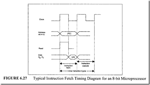
To execute an instruction, the microprocessor reads or fetches the op-code via the data bus from a memory location in the ROM/RAM external to the microprocessor. It then places the op-code (instruction) in the instruction register. Finally, the microprocessor executes the instruction. Therefore, the execution of an instruction consists of two portions, instruction fetch and instruction execution. We will consider the instruction fetch, memory READ and memory WRITE timing diagrams in the following using a single clock signal. Figure 6.27 shows a typical instruction fetch timing diagram.
In Figure 6.27, to fetch an instruction, when the clock signal goes to HIGH, the microprocessor places the contents of the program counter on the address bus via the address pins A0-A15 on the chip. Note that since each one of these lines A0-A15 can be either HIGH or LOW, both transitions are shown for the address in Figure 6.27. The instruction fetch is basically a memory READ operation. Therefore, the microprocessor raises the signal
on the READ pin to HIGH. As soon as the clock goes to LOW, the logic external to the microprocessor gets the contents of the memory location addressed by A0-A15 and places them on the data bus D0-D7. The microprocessor then takes the data and stores it in the instruction register so that it gets interpreted as an instruction. This is called "instruction fetch." The microprocessor performs this sequence of operations for every instruction.
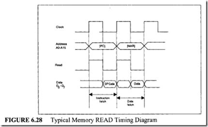
We now describe the READ and WRITE timing diagrams. A typical READ timing diagram is shown in Figure 6.28. Memory READ is basically loading the contents of a memory location of the main ROM/RAM into an internal register of the microprocessor. The address of the location is provided by the contents of the memory address register (MAR). Let us now explain the READ timing diagram of Figure 6.28 as follows:
1. The microprocessor performs the instruction fetch cycle as before to READ the op code.
2. The microprocessor interprets the op-code as a memory READ operation.
3. When the clock pin signal goes to HIGH, the microprocessor places the contents of the memory address register on the address pins A0-A15 of the chip.
4. At the same time, the microprocessor raises the READ pin signal to HIGH.
5. The logic external to the microprocessor gets the contents of the location in the main ROM/RAM addressed by the memory address register and places them on the data bus.
6. Finally, the microprocessor gets this data from the data bus via its pins D0 – D7 and stores it in an internal register.
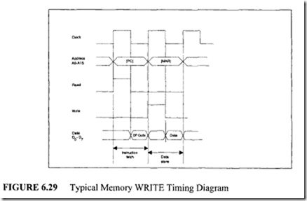
Memory WRITE is basically storing the contents of an internal register of the microprocessor into a memory location of the main RAM. The contents of the memory address register provide the address of the location where data is to be stored. Figure 6.29 shows a typical WRITE timing diagram. It can be explained in the following way:
l. The microprocessor fetches the instruction code as before.
2. The microprocessor interprets the instruction code as a memory WRITE instruction and then proceeds to perform the DATA STORE cycle.
3. When the clock pin signal goes to HIGH, the microprocessor places the contents of the
memory address register on the address pins A0-A15 of the chip.
4. At the same time, the microprocessor raises the WRITE pin signal to HIGH.
5. The microprocessor places data to be stored from the contents of an internal register onto the data pins D0-D7•
6. The logic external to the microprocessor stores the data from the register into a RAM
location addressed by the memory address register.
6.4.4 Memory Organization
Microcomputer memory typically consists of ROMs I EPROMs, and RAMs. Because RAMs can be both read from and written into, the logic required to implement RAMs is more complex than that for ROMs I EPROMs. A microcomputer system designer is normally interested in how the microcomputer memory is organized or, in other words, how to connect the ROMS IEPROMs and RAMs and then determine the memory map of the microcomputer. That is, the designer would be interested in finding out what memory locations are assigned to the ROMs I EPROMs and RAMs. The designer can then implement the permanent programs in ROMs I EPROMs and the temporary programs in RAMs. Note that RAMs are needed when subroutines and interrupts requiring stack are desired in an application.
As mentioned before, DRAMs (Dynamic RAMs) use MOS capacitors to store information and need to be refreshed. DRAMs are inexpensive compared to SRAMs, provide larger bit densities and consume less power. DRAMs are typically used when memory requirements are 16k words or larger. DRAM is addressed via row and column addressing. For example, one megabit DRAM requiring 20 address bits is addressed using 10 address lines and two control lines, RAS (Row Address Strobe) and CAS (Column Address Strobe). To provide a 20-bit address into the DRAM, a LOW is applied to RAS and 10 bits of the address are latched. The other 10 bits of the address are applied next and CAS is then held LOW.
The addressing capability of the DRAM can be increased by a factor of 4 by
![]()
![]() adding one more bit to the address line. This is because one additional address bit results into one additional row bit and one additional column bit. This is why DRAMs can be expanded to larger memory very rapidly with inclusion of additional address bits. External logic is required to generate the RAS and CAS signals, and to output the current address bits to the DRAM.
adding one more bit to the address line. This is because one additional address bit results into one additional row bit and one additional column bit. This is why DRAMs can be expanded to larger memory very rapidly with inclusion of additional address bits. External logic is required to generate the RAS and CAS signals, and to output the current address bits to the DRAM.
DRAM controller chips take care of refreshing and timing requirements needed by the DRAMs. DRAMs typically require 4 millisecond refresh time. The DRAM controller performs its task independent of the microprocessor. The DRAM controller sends a wait signal to the microprocessor if the microprocessor tries to access memory during a refresh cycle.
Because of large memory, the address lines should be buffered using 74LS244 or 74HC244 (Unidirectional buffer), and data lines should be buffered using 74LS245 or 74HC245 (Bidirectional buffer) to increase the drive capability. Also, typical multiplexers such as 74LS157 or 74HC157 can be used to multiplex the microprocessors address lines into separate row and column addresses.
6.5 Input/Output
Input/Output (I/O) operation is typically defined as the transfer of information between the microcomputer system and an external device. There are typically three main ways of
transferring data between the microcomputer system and the external devices. These are programmed I/O, interrupt I/O, and direct memory access. We now define them.
-
Programmed I/O. Using this technique, the microprocessor executes a program to perform all data transfers between the microcomputer system and the external devices. The main characteristic of this type of 110 technique is that the external device carries out the functions as dictated by the program inside the microcomputer memory. In other words, the microprocessor completely controls all the transfers.
-
Interrupt I/O. In this technique, an external device or an exceptional condition such as overflow can force the microcomputer system to stop executing the current program temporarily so that it can execute another program, known as the "interrupt service routine." This routine satisfies the needs of the external device or the exceptional condition. After having completed this program, the microprocessor returns to the program that it was executing before the interrupt.
-
Direct Memory Access (DMA). This is a type of I/O technique in which data can be transferred between the microcomputer memory and external devices without any microprocessor (CPU) involvement. Direct memory access is typically used to transfer blocks of data between the microcomputer’s main memory and an external device such as hard disk. An interface chip called the DMA controller chip is used with the microprocessor for transferring data via direct memory access.
