Quick and Dirty Logic Gates
One of the most frustrating aspects of designing digital electronic circuits is that when you are almost finished, you often discover that you are a gate or two short and you are left with the question of whether or not you should add another chip to the circuit. The major problem with adding another chip to the circuit is the requirement for additional space to place the chip in the circuit. Along with the need for additional space, adding another chip will add to the costs of the application and the difficulty in assembling it. In Chapter 2, I discussed that by using the Boolean arithmetic laws and rules, you could produce various functions using different gates than the ones that are ‘‘best suited’’ for the requirements. In the cases where there are no leftover gates available, a gate can be ‘‘cobbled’’ together with a few resistors, diodes and maybe a transistor. These simple gates are often referred to as being ‘‘MML’’ or ‘‘Mickey Mouse logic’’ technology because they can generally be used in most situations and with different logic families when a quick and dirty solution is required.
To be used successfully, they must be matched to the inputs and outputs of the different logic families that you are using and should not result in long switching times, which will affect the operation of the application, or large current draws, which could damage other components. As a rule of thumb, do not use one of the simple gates presented here between differing
technology gates; you will find that operation of different technologies can often be incompatible when you are adding resistors, diodes and transistors like the ones used in the sample gates presented here. Another rule of thumb is to make sure that each MML gate only drives one input – you can get into trouble with input fan-outs and multiple gate current sinking requirements very quickly. Along with trying to satisfy these requirements, there are cases where you will find that the MML gate will require at least as many pins as adding another chip and will be more difficult to wire. Generally speaking, adding MML gates to your application should be considered a ‘‘last’’ resort, not something you design in right from the start.
The most basic MML gate is the ‘‘inverter’’ and should not be a surprise.
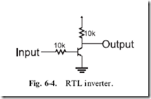
Figure 6-4 shows the circuit for the MML inverter, built out of two 10 k resistors and an NPN transistor. This inverter is actually a basic ‘‘RTL’’ (resistor–transistor logic) technology device and outputs a high voltage, when it is not being driven by any current. When current is passed to the gate, the transistor turns on and the output is pulled to ground (with good current sinking capability).
This circuit (as well as the other MML gates I discuss in this section) cannot handle high voltage or current inputs and outputs as well as commercially available logic gates and need to be ‘‘buffered’’. The need for buffering the MML’s gate inputs and output is an important point to note when considering using an MML gate in an application. As a rule, MML gates must be placed in the middle of a logic ‘‘string’’ rather than at the input or output ends to ensure that if you are expecting certain characteristics (such as the ability to drive a LED), standard TTL or CMOS technology gates will provide you with it.
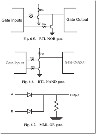
The inverter circuit can be simply modified by adding another transistor and resistor, as shown in Fig. 6-5, to create an RTL NOR gate. The RTL NAND gate is shown in Fig. 6-6. The NOR gate is considered the basis of RTL technology.
Implementing an AND or OR gate in MML is a bit more complex and requires a good understanding of the input/output parameters
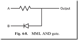
of the logic families. In Fig. 6-7, I have shown a sample design for an OR using two diodes and a resistor. The use of a 470 ohm resistor is probably surprising, but it was chosen to allow the gate to be used with both CMOS and TTL logic. In this case, if neither input has a high voltage, then the output will pull the input to ground. If the input is a CMOS gate, then the input will behave as if it were tied to ground. The 470 ohm resistor will allow the TTL input current to pass through ground and it will behave as if the input was at a low logic level. When the resistor is connected to a CMOS input, it will be effectively tying the input to ground, even though no current is flowing through it. In either case, when one of the inputs is driven high, the input pin will be held high and the gate connected to the output of the OR gate will behave as if a high logic level was applied to it.
An MML AND gate (Fig. 6-8) is the simplest in terms of the number of components. The diode and resistor work together to provide a high voltage
when both inputs are high, but when one of them is pulled low, the voltage level will be pulled down and current drawn from the input gate it is connected to.
While the MML AND presented in Fig. 6-8 will work in virtually any application, you may find that you will want to use a 470 ohm resistor in the circuit and a 10 k one in CMOS logic applications. The reason for doing this is to minimize the current drawn by the application; with a 470 ohm resistor, roughly 10 mA will be drawn when the output of the gate is low. This current draw decreases to 100 mA when a 10 k resistor is used instead for the resistors in these two gates.
Dotted AND and Tri-State Logic Drivers
You may feel constrained by the rule that you can only have one driver on a single line (or net). In Chapter 3, I introduced you to the concept of the ‘‘dotted AND’’ bus in which there was a common pull up on the net along with a number of transistor switches, each one of which could ‘‘pull’’ the net to a low voltage/logic level (and draw the current from any TTL gates inputs connected to the dotted AND). The dotted AND works reasonably well and has the advantage that it can control output voltages greater than the power applied to the logic chips. Some more subtle advantages are that more than one output can be active (tying the net to ground) and the operation of the bus will not be affected and TTL open collector and CMOS logic open drain outputs can be placed on the bus along with mechanical switches and other devices which can pull the bus to ground.
The dotted AND bus’s main disadvantage is its inability to source significant amounts of current. Smaller value pull up resistors can be used, but this increases the amount of current passed to ground when one of the open collector transistors is on. The dotted AND can be considered to be quite inefficient if it is low for a long period of time, because it is passing current directly to ground. The inability to source large amounts of current
is a drawback when high-speed signals are involved is the major disadvantage of the dotted AND bus. Changing an input from a high to a low, especially when there are some relatively large capacitances on the net, the switching time can become unreasonably slow.
A common error made by new circuit designers when they are adding a dotted AND bus to their designs is forgetting to add the pull up resistor. If the resistor has been forgotten, then the bus will never have a ‘‘high’’ voltage (although it will have a ‘‘low’’ voltage that can be detected). You will find that TTL inputs connected to a dotted AND but not having a pull up will work correctly, but CMOS logic inputs will not.
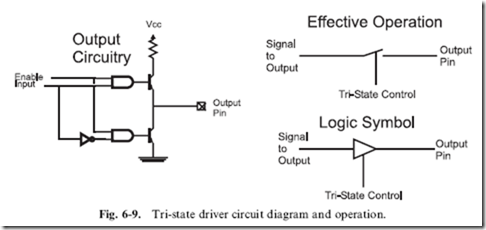
Another solution to the problem of wanting to have multiple drivers on the same net is to use ‘‘tri-state’’ drivers (Fig. 6-9). These drivers can ‘‘turn off’’ the transistors as effectively as if a switch were opened (the diagram marked ‘‘Effective Operation’’ in Fig. 6-9).
The left-hand side of circuit diagram of Fig. 6-9 shows how the tri-state driver works. If the tri-state control bit is inactive, the outputs of the two AND gates will always be low and the NPN output transistors can never be turned on. This ‘‘inactive’’ state is also known as the ‘‘high impedance state’’. When the tri-state control bit is active, then a high to either the top or bottom NPN transistor will allow the output to behave as an ordinary TTL output.
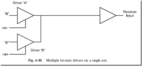
This ability to ‘‘turn off’’ allows multiple drivers, such as I have shown in Fig. 6-10, to be wired together. In this case, if data was to be placed on the net from Driver ‘‘B’’, the ‘‘Ctrl A’’ line would become inactive (the ‘‘high impedance state’’), followed by the ‘‘Ctrl B’’ line becoming active. At this point, the bus would be driven with the data coming from Driver ‘‘B’’.
It is important that only one tri-state driver is active at one time because the voltage on the common net will be indeterminate, as will be the logic level. You may be thinking that the term ‘‘indeterminate’’ to be the case when two drivers are active and are attempting to drive the net at different levels. This is true, but it is often also the case if two different drivers are driving at the same level: CMOS logic and TTL drivers will attempt to drive the net to different voltage levels and even TTL will not give repeating answers when you are trying to understand what is happening. The technical term for the situation where two tri-state drivers are active at the same time is ‘‘bus contention’’ and it should be avoided at all costs – only one driver should be active on the net at any one time.
At the start of this section, I noted that there could be more than one output active on a net at the same time. Note that when I say ‘‘multiple active outputs’’, I mean more than one driver pulling the net low. I do not recommend this to be part of the design, however; multiple active outputs are impossible to differentiate and you will have problems figuring out which bits are active and what signal is being sent (with multiple outputs active, state changes from one output will most likely be masked by the active operation of others).
Before leaving this section, I do want to point out that tri-state drivers can be used on a dotted AND bus. This is probably surprising, considering the dire warnings I have put in regarding bus contention. The trick to adding a tri-state driver to a dotted AND bus is that it is normally disabled and only a low voltage can be put on the net by the tri-state driver. High values are output by simply disabling the tri-state driver and letting the net’s pull up provide the high voltage. Combining Functions on a Net
As a purely intellectual exercise, it can be interesting to see how many functions you can build into a single digital electronics net. From a practical point of view, cramming multiple functions on a single line will minimize the amount of effort that must be expended to build a prototype application. Many products carry out multiple functions on a single line; generally, this is done to allow the manufacture and sale of simpler products. Whatever the motivation, ‘‘stretching’’ a logic technology to allow multiple functions on a single net requires a strong knowledge of the technology’s electrical parameters and the technology’s normal operating conditions. The most important thing to remember is that the input/output devices attached to the net must be properly coordinated to make sure that data is read and written at the right times.
The most obvious ways of connecting two drivers together is to use dotted AND and tri-state drivers on a ‘‘bus’’, as I discussed in the previous section.
These methods work well and should be considered as the primary method of implementing multiple devices on the net. The other methods discussed here work best for specific situations; but there is no reason why you can’t modify your design to take advantage of these specific instances.
When interfacing the bi-directional digital I/O pin to a CMOS driver and a CMOS receiver (such as a memory with separate output and input pins), a resistor can be used to avoid bus contention at any of the pins, as is shown in Fig. 6-11. Using this wiring, when the bi-directional I/O pin is driving an output, it will be driving the ‘‘Data In’’ pin register, regardless of the output of the ‘‘Data Out’’ pin. If the bi-directional and ‘‘Data Out’’ pins are driving different logic levels, the resistor will limit the current flowing between the bi-directional and the memory ‘‘Data Out’’ pin. The value received on the ‘‘Data In’’ pin will be the bi-directional device’s output.
When the bi-directional digital I/O is receiving data from the memory, ![]() the I/O pin will be put in ‘‘input’’ (or ‘‘high impedance’’) mode and the
the I/O pin will be put in ‘‘input’’ (or ‘‘high impedance’’) mode and the
‘‘Data Out’’ pin will drive its value to not only the bi-directional device’s I/O pin, but the ‘‘Data In’’ pin, as I noted above. In this situation, the ‘‘Data In’’ pin should not be latching any data in; the simplest way to ensure this is to make the digital I/O pin part of the I/O control circuitry. This is an important point because it defines how this circuit works. A common use for this method of connection data in and data out pins is used in memory chips that have separate data input and output pins.
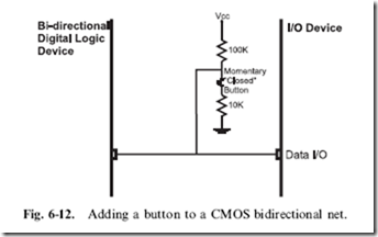
User buttons can be placed on the same net as logic signals as Fig. 6-12 shows.
When the button is open or closed, the bi-directional logic device can drive data to the input device, the 100 k and 10 k resistors will limit the current flow between Vcc and ground. If the bi-directional logic device is going to read the button ‘‘high’’ (switch open) or ‘‘low’’ (switch closed) it will be driven on the bus at low currents when the pin is in ‘‘Input Mode’’. If the button switch is open, then the 100 k resistor acts like a ‘‘pull up’’ and a ‘‘1’’ is returned. When the button switch is closed, there will be approximately a half volt across the 10 k resistor, which will be read as a ‘‘0’’.
The button with the two resistors tying the circuit to power and ground is
like a low-current driver and the voltage produced is easily ‘‘overpowered’’ by active drivers. Like the first method, the external input device cannot receive data except when the bi-directional device is driving the circuit. A separate clock or enable should be used to ensure that input data is received when the bi-directional device is driving the line.
This method of adding a button to a net can be extrapolated to work with a switch matrix keyboard (presented later in the book), although the circuit and interface operation will become quite complex. Secondly, a resistor/ capacitor network for ‘‘debouncing’’ the button cannot be used with this circuit as it will ‘‘slow down’’ the response of the bi-directional device driving
the data input pin and will cause problems with the correct value being accepted.
For both of these methods of providing multiple features to a single net, you should only use CMOS logic as it is voltage controlled and not current controlled, like TTL. You may be able to use TTL drivers with these circuits, but they may be unreliable. To avoid problems with invalid currents being available to TTL receivers, just use the latter two circuits with CMOS digital logic.
Designing a circuit in which multiple functions are provided on a single net
for an application is not always possible or even desirable. Like any design feature implemented in an application, before trying to combine multiple functions on a single net, you should understand the benefits as well as the costs. When it is possible, you can see some pretty spectacular results; my personal record was for a LCD driver in which I was able to combine five functions on a single net – LCD Data Write, LCD Data Read, Data In Strobe, Data Ready Poll and configuration switch poll.
Quiz
1. What parameter is not listed in the chip characteristic card?
(a) Input fanout
(b) Number of gates built into the chip
(c) Electrical dependencies
(d) Maximum operating speed
2. What is not a typical digital electronic output pin type?
(a) Totem pole
(b) Open collector
(c) High-current
(d) Tri-state driver
3. Other than the XOR gate, are any other of the six basic I/O gates capable of producing race conditions just by themselves?
(a) Each one is capable of producing a race condition under certain circumstances
(b) The NOR Gate in TTL
(c) The AND Gate in CMOS Logic
(d) No
4. What is not a factor in determining if a marginal circuit and component will produce a race condition?
(a) Ambient temperature
(b) Net length
(c) Power voltage
(d) The phases of the moon
5. Mickey Mouse logic should be used:
(a) Never
(b) When you are in a hurry to get the application finished
(c) When you have board space, cost and available gate constraints that preclude adding a standard chip
(d) When there is a need to pass a CMOS output to a TTL input
6. Each item is an advantage of a dotted AND bus except:
(a) The dotted AND bus can have tri-state drivers on it as well as mechanical switches
(b) The dotted AND bus can control voltages greater than the chip’s Vdd/Vss
(c) The dotted AND bus is cheaper than one manufactured with tri-state drivers
(d) The dotted AND bus can consist of CMOS logic as well as TTL drivers
7. When tri-state drivers are inactive, another term that is used to describe the state is:
(a) High resistance
(b) High impedance
(c) Low current output
(d) Driver isolation
8. When should multiple tri-state drivers be active?
(a) When more current is required on the net
(b) When more speed is required on the net
(c) When the receiver detects an ambiguous logic level
(d) Never
9. When adding a push button to a net, can the 100 k resistor connected to positive power and the 10 k resistor connected to positive power be swapped?
(a) Yes
(b) No
(c) Only if TTL receivers and drivers are used.
(d) Yes, if you can ensure that the signals passing between the digital devices are still within specified operating margins.
10. When putting a receiver and driver on the same net, can the current limiting resistor be wired between the bi-directional logic device and the ‘‘Data In’’ pin, leaving a direct connection between the bi-directional logic device and ‘‘Data Out’’?
(a) Yes. There aren’t any cases where it wouldn’t work
(b) Yes, if the resistor value is within 1 k and 10 k
(c) Yes, for certain technologies of CMOS logic
(d) No. This will cause bus contention
