Latches Versus Registers
Two terms that are often used interchangeably are ‘‘register’’ and ‘‘latch’’. In the previous section, I introduced you to the ‘‘register’’, which is another
term for an edge triggered flip flop. When you look at parts lists and datasheets, you will see parts that are identified as ‘‘registers’’ and others as ‘‘latches’’ and these parts will have the same pinouts with no obvious differentiation in operation between the devices. Furthermore, I have found many chip manufacturers that have labeled their parts as ‘‘latches’’ when in fact they were ‘‘registers’’ and vice versa.
Quite simply put, ‘‘registers’’ are flip flops that store data when the rising (low to high or 0 to 1) or falling (high to low or 1 to 0) edge (whichever is used by the device) is received on the ‘‘clock’’ (or, my abbreviation, ‘‘Clk’’) pin. Registers are aptly named because they are normally used as simple data storage devices for microprocessor memory.
Latches are often used in microprocessor applications to save an address on a multi-purpose bus.
The best analogy for the ‘‘latch’’ that I can think of is a latch on a barn door: when the latch is not engaged, animals and whatever can wander in.
Once the latch is closed, what is in the barn stays in. The ‘‘latch’’ flip flop works similarly to this; with one state of the clock line, the input data is passed to the output directly and can be changed at any time (i.e. there isn’t any storage) but once the clock line changes state, the last value of the data is stored in the latch until the clock changes value.
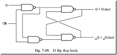
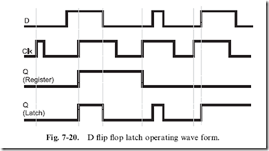
In the previous section, I introduced you to the edge triggered D flip flop ‘‘registers’’. The D flip flop ‘‘latch’’ is actually quite a bit simpler (Fig. 7-19), but what is interesting about it is that it doesn’t work anything like its edge triggered cousin. In Fig. 7-20, I have drawn a data input along with a clock and the ‘‘Q’’ (output pin) values for an edge-triggered D flip flop register and a D flip flop latch.
You will probably be surprised to see that waveforms for the two memory devices are completely different. The edge triggered D flip flop register ![]() stores data in a very consistent and logical way – every time the clock pin
stores data in a very consistent and logical way – every time the clock pin
rises, the value of ‘‘D’’ is stored in the flip flop and nothing changes until the next rising edge of the clock pin.
The latch, on the other hand, seems to operate more like an AND gate than a memory storage device. The storage function tends to be obfuscated in the example of Fig. 7-20 because in many cases, I show the D pin changing state before the clock line returns low. This is an important point because many people consider the two devices to be interchangeable and this is simply not the case. Latches and registers have different applications and it is critical for you to understand what they are. You cannot put a latch chip in place of a register simply because they are pin compatible; you must make sure that the incoming data does not change state until the clock goes low.
Interestingly enough, latches do not need as much time to save data as a register; there are 9 fewer gate levels for a signal to pass through and even though I show the data save operations being instantaneous in Fig. 7-20, they are not. The latch can take as little as one-third of the time to save data as a register and only requires two gate delays before passing the data along (after which the data can be stored). This makes the latch an important chip for working with microprocessors with a ‘‘multiplexed’’ address bus.
Reset
If you cycle the power to any flip flop, you will have noticed that the initial ‘‘state’’ (or value) can be either ‘‘0’’ (LED off) or ‘‘1’’ (LED on), with no way of predicting which value it will be. This is normal because when power is applied to the flip flop it will start executing in the metastable state, and for any kind of imbalance in the circuit (e.g. residual charge or induced voltage) on the inputs of either NAND/NOR gate, the flip flop will respond and this will be its initial state. Often, this random initial state is not desired – instead, the circuitry should power up into a specific known state for it to work properly. This is why throughout this chapter I have taken pains to note that the initial state of a flip flop is not known. You may find that an application with one flip flop usually powers up the same way; if you were to do a statistical analysis of the power up values, you might even find that a single power up state approaches 100%, but you cannot guarantee this for all occurrences of the chip, or even that all other similar chips in the same application circuit will power up the same way.
Specifying the state when the circuit is powered up is known as ‘‘initialization’’ (just as it is for programming) and is required for more than just sequential logic circuits. Initialization normally takes place when the application is ‘‘reset’’, or waiting to start executing. To avoid confusion later, I should point out there are two types of ‘‘reset’’ described in this book when I talk about digital circuits. Earlier, when I was talking about simple combinatorial circuits, I also called a ‘‘low’’ or ‘‘0’’ voltage level ‘‘reset’’ (and ‘‘high’’ or ‘‘1’’ as ‘‘set’’). Now, when the term ‘‘reset’’ is used, I am describing the state when the circuit is first powered up or stopped to restart it from the beginning. When you read the term ‘‘reset’’ later in the book (as well as in other books), remember that if a single bit or pin is being described, the term ‘‘reset’’ means that it is ‘‘0’’ or at a low level. If a sequential circuit (like a microcontroller) is ‘‘held reset’’ or ‘‘powering up from reset’’, I mean that it is being allowed to execute from a known state.
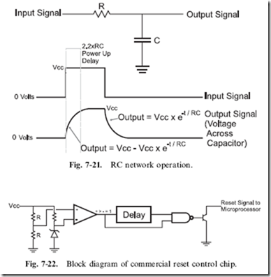
The ‘‘_CLR’’ pin on the full D flip flop (like the 7474) is known as a ‘‘negative active control’’ and is active when the input is at a ‘‘0’’ logic level. To make this pin active during power up, yet allow the chip to function normally, a resistor/capacitor network on the TTL input pin delays the rise of the pin (as shown in Fig. 7-21) so that the pin is active low while power is good. When the signal on ‘‘_CLR’’ goes high, and the clear function is no longer active, the chip can operate normally, with it being in an initial known state.
The time for the RC (resistor/capacitor) network to reach the threshold voltage can be approximated using the equation:
When you work with microprocessors and microcontrollers, you will want to implement a more sophisticated reset circuit. Many microprocessor manufacturers recommend an analog comparator based reset circuit like the one shown in Fig. 7-22. This circuit controls an open collector (or open drain)
transistor output pin that will pull down a negative active reset pin when power dips below some threshold value. This circuit is often available as a ‘‘processor reset control’’ chip and is put into the same black plastic package as a small transistor (known as a TO-92).
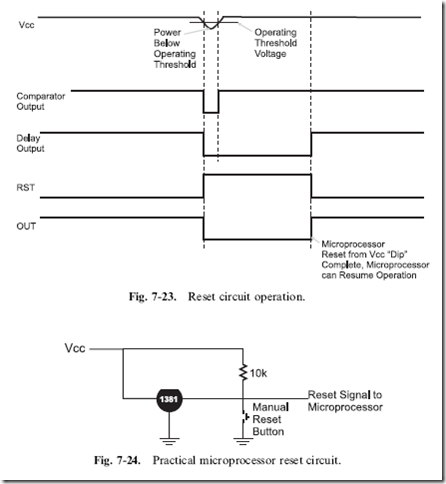
Processor reset control chips are available for a very wide variety of different ‘‘cut off ’’ voltages, ranging from 2.2 volts and upwards. Figure 7-23 shows the operation of the internal parts of the processor reset control chip when the input voltage drops below the set value; the comparator stops outputting a ‘‘1’’ and a delay line is activated. This delay line is used to filter out any subsequent ‘‘glitches’’ in the power line and makes sure that the power line is stable before allowing the processor to return from reset and continue executing. When the comparator outputs a low value or the delay line is continuing to output a low value, the output of the NAND gate they are connected to is high and it turns on the open collector output transistor, pulling the circuit to ground.
The Panasonic MN1381 line of chips is a very popular processor reset control and can be used to control a sequential circuits reset using
a circuit similar to the one shown in Fig. 7-24. This circuit will take advantage of the RC network delaying the rise of the control signal, provide you with the ability to reset or stop the operation of the micro- processor and halt the operation of the robot if the battery falls below a safe minimum.
If you power on and off a circuit quickly, you may find that it does not power up properly. This is due to the capacitor in the reset circuit not discharging fully – it may take as much as 10 seconds for it to discharge completely. This was actually an issue with the original IBM PC; if you had a situation where the PC ‘‘hung’’, you would have to power down and wait at least 15 seconds to make sure that the reset circuit would allow the computer to power up properly.
Quiz
1. Feedback in digital electronics:
(a) Is built into every gate
(b) Must always be avoided
(c) Can be used to store bit data
(d) Is only used in radio interface circuitry
2. Ring oscillators can be used:
(a) In digital watches
(b) To measure the gate delay of a logic technology
(c) To test the operation of a combinatorial circuit
(d) Only when current limiting resistors are in place to protect gate outputs
3. What do the letters ‘‘R’’ and ‘‘S’’ stand for in the RS flip flop?
(a) ‘‘Recessive’’ and ‘‘Static’’
(b) ‘‘Reset’’ and ‘‘Set’’
(c) ‘‘Rothchild’’ and ‘‘Stanislav’’
(d) ‘‘Receive’’ and ‘‘Send’’
4. What is the ‘‘metastable state’’ of a flip flop?
(a) When it has started to oscillate
(b) The time between when the inputs change the output is correct
(c) The state in which the outputs of a flip flop are half way between ‘‘0’’ and ‘‘1’’ and can be easily ‘‘pushed’’ into a specific state
(d) The state in which ‘‘Q0’’ is unknown
5. ‘‘Toggling’’ a bit means:
(a) Setting (making the output a 1) of a bit
(b) Leaving the bit in its current state
(c) Inverting the bit’s state
(d) Resetting (making the output a 0) of a bit
6. A ‘‘Register’’ can be used in:
(a) Nowhere, it is a thought experiment used to show feedback in a digital application
(b) Just computer processors
(c) Just sequential digital electronics application
(d) Just about any digital electronics application
7. The ‘‘_Pre’’ pin of a D flip flop will:
(a) Set the bit
(b) Reset the bit
(c) Nothing
(d) Toggle the state of the bit
8. Which formula specifies the RC network response to a sudden voltage input?
9. Why are latches like barn doors?
(a) They provide a secure environment for what’s inside them
(b) They are both relatively heavy
(c) They allow free passage until the latch is engaged
(d) They are the fastest method for passing things in and out
10. Which application is a latch best suited for?
(a) Main memory in a computer system
(b) Bicycle lock combinations
(c) Stopping and saving data mid-stream
(d) Temporary storage of data in a microprocessor


