Data Transfer Techniques: Interfacing Memories and I/Os
1. Mention the two broad categories in which data transfer schemes are classified?
Ans. The data transfer schemes are broadly classified into two categories. These are
* Programmed data transfer
* Direct Memory Access (DMA) transfer.
2. Mention the types of programmed data transfer.
Ans. Programmed data transfer scheme is sub-divided into the following:
* Synchronous mode of data transfer,
* Asynchronous mode of data transfer and
*Interrupt driven mode of data transfer.
3. What are the features of programmed data transfer scheme?
Ans. In this scheme, data transfer takes place under the control of a program which resides in the main memory of the system. It is relatively slow and applied for cases when the number of bytes of data is small. This scheme is suitable for relatively slow peripherals.
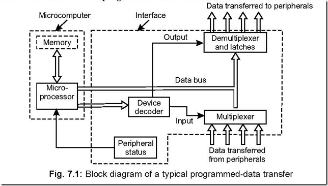
4. Explain with the help of a block diagram, a typical programmed data transfer scheme.
Ans. The block schematic of a programmed data transfer scheme is shown below:
For an input from or an output to a peripheral device, an I/O instruction is issued to a device decoder which therefore selects the corresponding multiplexer (for input) or demultiplexer (for output) respectively. The peripheral is tested for its readiness by means of a F/F. When the peripheral is ready, data from the peripheral goes to the accumulator of microprocessor or vice-versa for input or output peripherals respectively.
Since peripherals are usually slower than microprocessors, data are usually latched from the bus before actually handed over to the peripheral via the demultiplexer.
5. Mention and clarify the functions needed for peripheral interfacing.
Ans. The important functions are: buffering, address decoding, command decoding and timing and control.
Buffering is necessary to increase drive and also to synchronise data exchange between the microprocessor and peripheral.
A particular I/O is selected with the help of address decoding.
Command decoding is needed for some special I/Os that perform jobs other than data
transfers—e.g. rewinding a tape drive.
For coordinating the above three, timing and control is needed.
6. In how many categories the interfacing peripherals are classified. Ans. The interfacing peripherals are classified into two categories:
* General purpose peripherals.
*Special purpose peripherals.
7. Give some examples of general purpose and special purpose peripherals. Ans. Examples of some general purpose peripherals are:
* Input/output ports
* Programmable Interrupt Controller (PIC)
*Programmable interval timer
* Programmable communication interface
* Programmable DMA interface
* Multipurpose programmable device.
While some of the special purpose peripherals are:
* Programmable CRT controller
*Programmable floppy disk controller
* Programmable keyboard and display interface.
8. Why it is relatively easy to interface memories than I/O devices? Elaborate.
Ans. It is relatively easy to interface a memory with a processor because memories are usually manufactured with the same technology as those of the CPUs and they are compatible to the CPUs with regard to speed and electrical compatibility.
But when an I/O device is interfaced with a processor, the following incompatibilities may arrive. These are:
* Speed incompatibility.
* Format incompatibility.
* Electrical characteristic incompatibility.
The first incompatibility arises because in many cases the I/O devices are slower than the processor so that a situation may arise when the processor is in a position to accept data but the peripheral, because of its slow nature, is unable to provide valid data.
The second incompatibility may arise if a 12-bit or 16-bit ADC or DAC is tried to be interfaced with an 8-bit microprocessor like 8085.
The third incompatibility may be due to current or voltage incomparability or both. Thus if a 12 V relay is to be driven by the SOD pin of 8085—both incompatibilities would be there. First the voltage (5 V) from the SOD pin is to be boosted to 12 V and also the current required to drive the relay should be provided. Thus it needs buffering.
9. Discuss the synchronous mode of data transfer.
Ans. Synchronous mode of data transfer is performed for peripherals whose timing characteristics is precisely known. In this mode the status of the device is not checked before undertaking any data transfer, that means, the device is assumed to be ready when data transfer takes place. This scheme is simplest amongst all the methods and minimum overhead in terms of hardware/software is needed to implement this scheme.
The following two figures show the flowchart for the data transfer scheme in synchronous mode. Figure 7.2 (a) corresponds to the case when the peripheral is in speed compatible with the CPU, while Fig. 7.2(b) corresponds to slower peripherals. For both Figs. 7.2(a) and (b), the timing characteristics of the peripheral should exactly be known. For the case of Fig. 7.2(b), the CPU sends get ready’ signal to the peripheral, followed by a wait for a predetermined time by the CPU. The CPU then executes the I/O instruction for data transfer to take place effectively.
10. Discuss the asynchronous mode of data transfer scheme.
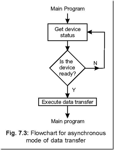
Ans. In this case the CPU initiates data transfer with the peripheral. The device (peripheral) status is checked by the CPU before undertaking data transfer. This mode is used when the timing characteristics of the device is unpredictable.
The flowchart for this scheme is shown in
Fig. 7.3.
In this mode, the CPU confirms the readiness of the device status before undertaking data transfer. This is why this scheme is known by the name “handshaking I/O”.
11. What is the main disadvantage of asynchronous mode of data transfer.
Ans. If there is an appreciable time gap from the instant the microprocessor starts checking the ‘device ready’ signal and its (device) actual readiness, the system loops the loop, as is evident from Fig. 7.3. This is a time simply wasted by the processor until the device is ready with valid data. In an unfortunate situation, the system may enter into an infinite loop if the device does not become ready at all.
12. Discuss the interrupt driven mode of data transfer.
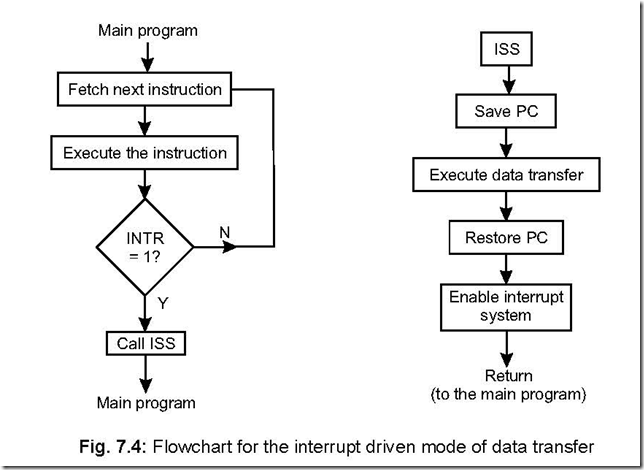
Ans. Main characteristic of this mode of data transfer is that data exchange between peripheral and the processor is initiated by the device.
This mode is used for data transfer with slow peripherals and also when the occurrence of data is unpredictable in nature.
The steps which are followed in this mode are:
* An interrupt is requested by a peripheral device.
* An acknowledgement of the request is issued by the processor at the end of the
execution of the current instruction.
* The program then branches to Interrupt Service Subroutine (ISS) program at which the program corresponding to the interrupting device is already stored. The return address (in the PC) is stored in the stack along with other register contents as per program needs.
* Data transfer takes place under ISS.
* Interrupt system is enabled.
* The program then returns to the main program after loading the return address from stack in program counter (PC).
The flowchart corresponding to this scheme is shown below:
13. How does the asynchronous system differ from the interrupt driven mode of data transfer?
Ans. Whereas in the asynchronous mode of data transfer scheme it is the processor which goes on checking the device status, in the interrupt driven mode of data transfer scheme it is the device which interrupts the system.
14. In how many categories are interrupt driven mode of data transfer scheme divided?
Ans. It is divided into two categories: Polled interrupt and vectored interrupt. Again polled interrupt can be of two types: software polling, hardware polling.
15. Explain polled interrupt system.
Ans. Polled interrupt can be of two types and is used when many devices are connected to the system. In a polled interrupt scheme (whether hardware or software), each device is tested, using either hardware or software, until the device which has requested the interrupt, is identified. Corresponding to the device thus identified, the program is then diverted to the ISS written for that device.
16. Compare polled interrupt versus vectored interrupt.
Ans. In polled interrupt scheme (whether hardware/software) the priority of each device is fixed (by the programmer). It will take time before the interrupting device is identified. On the other hand, in the vectored interrupt scheme the requesting device causes the program to be branched to the ISS straightway. Hence vectored interrupt schemes are, in general, faster than polled interrupt schemes.
17. Describe the hardware polling scheme.
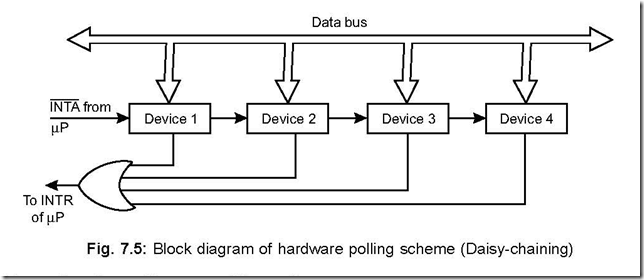
Ans. The schematic of a hardware polling scheme involving four devices is shown below. This scheme is also known as ‘daisy-chaining’. The four device status flags from the four
devices are ORed and taken to the INTR pin of the processor. A low INTA is issued by
the processor at the end of the current instruction execution. The INTA signal is passed
on to device 1—the highest priority device. If device 1 has interrupted the processor then
it will identify itself with the data bus. If not, the INTA signal is passed on to device 2
and so on. Thus it is apparent that device 4 has got the lowest priority.
18. Describe the software polling scheme.
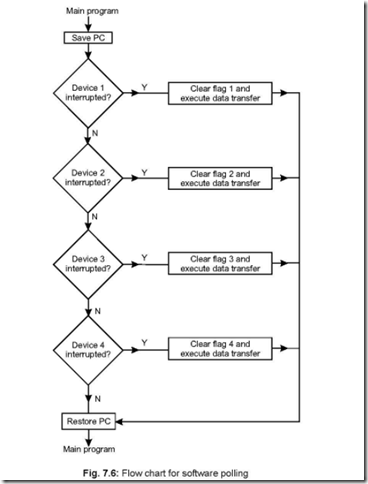
Ans. The flowchart for software polling scheme is shown below. It shows four devices whose status are checked in software one after the other. As per the scheme, device 1 has the highest priority while the lowest priority device is device 4. The status of each device are ORed and connected to INTR pin of the processor. On occurrence of an interrupt, the flag of each device is tested as per the software polling scheme.
19. Explain DMA (Direct Memory Access) mode of data transfer.
Ans. Instruction set of a processor provides for data transfer between processor registers and memory or I/O device. Thus when data transfer between memory and a I/O device is needed, it is done in two steps—from memory to accumulator of processor and then to I/O device or reverse. This slows down data transfer. DMA mode is introduced to overcome this.
In DMA mode, straight data exchange takes place between memory and I/O device bypassing the processor. This is done with the help of a DMA controller. In DMA mode, the DMA controller acts as a ‘Master’ and the processor as a ‘Slave’.
20. What features must the processor and the DMA controller have to ensure proper operation in DMA mode?
Ans. The processor must have the following features to facilitate DMA mode of data transfer:
z An input line through which the processor accepts request from DMA controller for DMA mode of data transfer (This is the ‘HOLD’ pin for mP 8085).
z An output line through which the processor tells the DMA controller that it (processor) has accepted the request (This is the ‘HLDA’ pin for mP 8085)
z The processor must tristate its AB, DB and necessary control lines before handing over the control to the DMA controller.
The DMA controller IC must have the following features:
z An output line through which it requests the processor for DMA mode of data transfer. z An input line through which it accepts the granted DMA request from the processor. z Control over the AB, DB and the necessary control lines.
21. What is meant by address space?
Ans. It is defined as the set of all possible addresses that a microprocessor can generate.
22. What is meant by address space partitioning?
Ans. 8085 microprocessor has a 16-bit address bus so that it can address 216 or 64 KB of address—called the address space of 8085. This total address space can be partitioned or allocated to memory or I/O devices so that they can be addressed properly. This is called address space partitioning.
23. What are the ways in which the address space can be partitioned? Ans. The address space can be partitioned in two ways. These are:
* Memory mapped I/O scheme.
* I/O mapped I/O scheme.
24. Describe the memory mapped I/O scheme.
Ans. In this scheme, there is only one address space. This address space is allocated to both memory and I/O devices. Some addresses are assigned to memories and some to I/O devices. The address for I/O devices is different from the addresses which have been assigned to memories. An I/O device is also treated as a memory location. In this scheme one address is assigned to each memory location and one address is assigned to each I/O device.
![]() In this scheme, all data transfer instructions of the microprocessor can be used for transferring data from and to either memory or I/O devices. For example, MOV D,M instruction would transfer one byte of data from a memory location or an input device to the register D, depending on whether the address in the H-L register pair is assigned to a memory location or to an input device. If H-L contains address of a memory location, data will be transferred from that memory location to register D, while if H-L pair contains the address of an input device, data will be transferred from that input device to register D.
In this scheme, all data transfer instructions of the microprocessor can be used for transferring data from and to either memory or I/O devices. For example, MOV D,M instruction would transfer one byte of data from a memory location or an input device to the register D, depending on whether the address in the H-L register pair is assigned to a memory location or to an input device. If H-L contains address of a memory location, data will be transferred from that memory location to register D, while if H-L pair contains the address of an input device, data will be transferred from that input device to register D.
This scheme is suitable for small systems. In this scheme, IO/ M signal is not used
to distinguish between memory and I/O devices. An I/O device is interfaced in the same manner as a memory device.
25. Explain the I/O mapped I/O scheme.
![]()
![]() Ans. Some CPUs provide one or more control lines (for example, IO/ M line for 8085), the status of which indicates either memory or I/O operation. When the status of IO/ M line
Ans. Some CPUs provide one or more control lines (for example, IO/ M line for 8085), the status of which indicates either memory or I/O operation. When the status of IO/ M line
is high, it indicates I/O operation and when low, it points to memory operation. Thus, in this case, the same address may be assigned to both memory or an I/O device—
æ
depending on the status of IO/M line.
The above scheme is referred to as I/O mapped I/O scheme. Here two separate address spaces exist—one space is meant exclusively for memory operations and the other for I/O operations. Usually, the space earmarked for I/O is much smaller than memory space.
26. Pictorially show the memory mapped I/O and I/O mapped I/O scheme.
Ans. The following figure shows, pictorially, both the schemes. Here it is assumed that the system has a 64 KB of memory and 256 I/O space.
27. What is another name of I/O mapped I/O and how many I/O’s can be accessed in this mode?
Ans. I/O mapped I/O is also known as standard I/O. A maximum of 28 = 256 I/Os can be addressed in this mode, because in this mode a 1-byte address is specified.
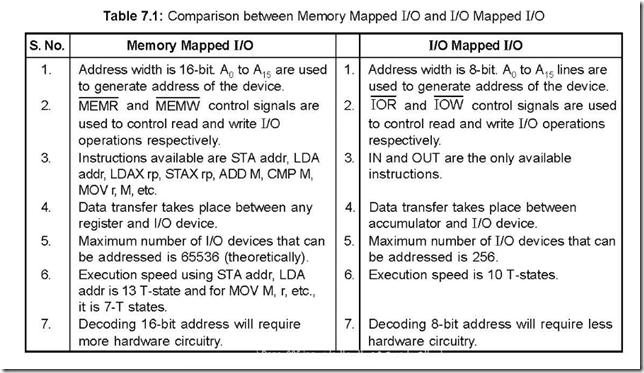
28. Bring out the distinguishing features between memory mapped I/O scheme and I/O mapped I/O scheme.
Ans. The following table shows the distinguishing features of the two schemes:
29. What are the instructions available in memory mapped I/O and I/O mapped I/O scheme?
Ans. The instructions available in memory mapped I/O scheme are LDA, LDAX, STA, STAX, MOV M, r etc. while those for I/O mapped I/O scheme are IN and OUT.
The CPU sends out an 8-bit code to identify the particular port address.
30. Mention the most important advantage of memory mapped I/O scheme over I/O mapped I/O scheme.
Ans. The main advantage of memory mapped I/O scheme is that all memory reference instructions are available in this scheme.
31. 2 KB RAM, 2 KB ROM, one input and one output device are to be interfaced with 8085 microprocessor. Employ memory mapped I/O scheme to execute the above.
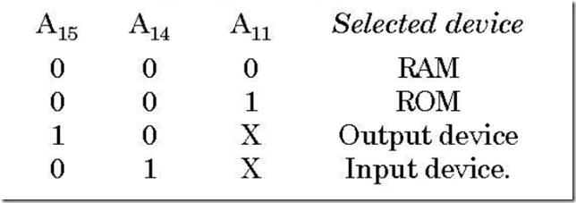
Ans. Total memory capacity: 2 KB RAM and 2 KB ROM = 4 KB. This requires 12 address lines (212 = 4 K). Out of 12, 11 address lines (A0 to A10) of mP are connected to 11 memory address lines. Address line A11 is used as chip select. The RAM chip is selected when A11 is low and ROM gets selected for A11 = 1.
The two address lines are connected to A15 and A14. Thus, the 16-bit address line
would be:
I represents I/O devices
C represents chip select
M represents memory
X represents don’t care.
Status of A15, A14 and A11 selects either memory or I/O devices as follows:
32. Employ I/O mapped I/O scheme for Q 31.
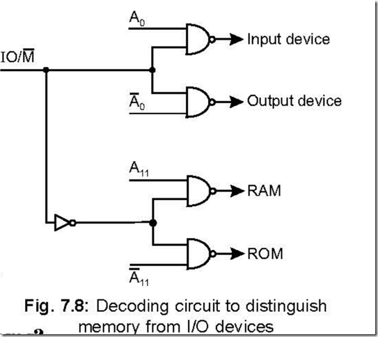
Ans. In this scheme, IO/ M signal distinguishes between an I/O and a memory.Memory addressing is done exactly in the same manner as discussed in Q 31 In this scheme, the input and output devices are identified by IO/ M along with A0 address line, while the RAM and ROM are identified by IO/ M signal along with A11 address line. The scheme of decoding is shown in Fig. 7.8.
33. Why WAIT states are used in μC based systems?
Ans. WAIT states are used to interface slow peripherals to the processor.
