External Memory
The system designer is not limited by the amount of internal RAM and ROM available on chip. Two separate external memory spaces are made available by the 16-bit PC and DPTR and by different control pins for enabling external ROM and RAM chips. Internal control circuitry accesses the correct physical memory, depending upon the machine cycle state and the opcode being executed.
There are several reasons for adding external memory, particularly program memory, when applying the 8051 in a system. When the project is in the prototype stage, the expense-in time and money-of having a masked internal ROM made for each program "try" is prohibitive. To alleviate this problem, the manufacturers make available an EPROM version, the 8751, which has 4K of on-chip EPROM that may be programmed and erased as needed as the program is developed. The resulting circuit board layout will be identical to one that uses a factory-programmed 8051. The only drawbacks to the 8751 are the specialized EPROM programmers that must be used to program the non-standard 40-pin part, and the limit of "only" 4096 bytes of program code.
The 8751 solution works well if the program will fit into 4K bytes. Unfortunately, many times, particularly if the program is written in a high-level language, the program size exceeds 4K bytes, and an external program memory is needed. Again, the manufacturers provide a version for the job, the ROMless 8031. The (EA)’ pin is grounded when using the 8031, and all program code is contained in an external EPROM that may be as large as 64K bytes and that can be programmed using standard EPROM programmers.
External RAM, which is accessed by the DPTR, may also be needed when 128 bytes of internal data storage is not sufficient. External RAM, up to 64K bytes, may also be added to any chip in the 8051 family.
Connecting External Memory
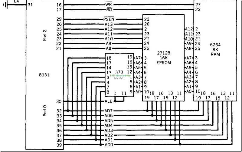
Figure 8 shows the connections between an 8031 and an external memory configuration consisting of 16K bytes of EPROM and 8K bytes of static RAM. The 8051 accesses external RAM whenever certain program instructions are executed. External ROM is accessed whenever the EA(external access) pin is connected to ground or when the PC contains an address higher than the last address in the internal 4K bytes ROM (OFFFh). 8051 designs can thus use internal and external ROM automatically; the 8031 , having no internal ROM, must have (EA)’ grounded.
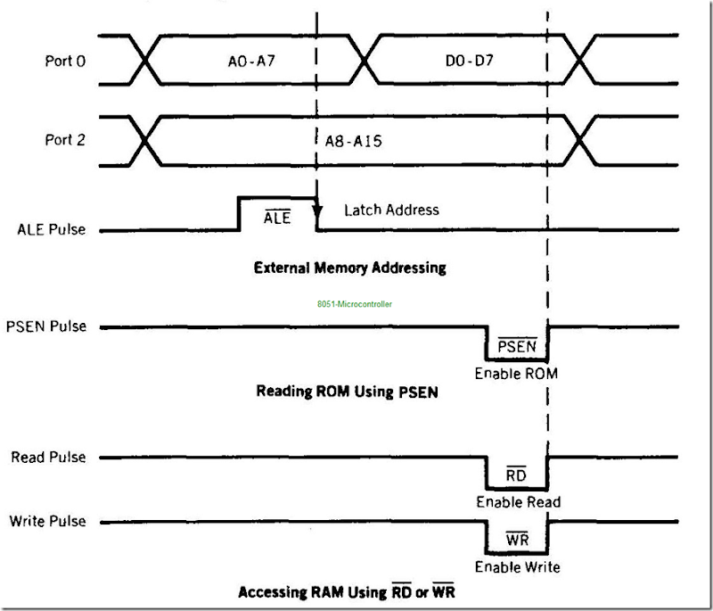
Figure 9 shows the timing associated with an external memory access cycle. During any memory access cycle, port 0 is time multiplexed. That is, it first provides the lower byte of the 16-bit memory address, then acts as a bidirectional data bus to write or read a byte of memory data. Port 2 provides the high byte of the memory address during the entire memory read/write cycle.
The lower address byte from port 0 must be latched into an external register to save the byte. Address byte save is accomplished by the ALE clock pulse that provides the correct timing for the 373 type data latch. The port 0 pins then become free to serve as a data bus.
If the memory access is for a byte of program code in the ROM, the (PSEN)'(program store enable) pin will go low to enable the ROM to place a byte of program code on the data bus. If the access is for a RAM byte, the (WR)'(write) or (RD)'(read) pins will go low, enabling data to flow between the RAM and the data bus.
The ROM may be expanded to 64K by using a 27512 type EPROM and connecting the remaining port 2 upper address lines A14-A15 to the chip.
At this time the largest static RAMs available are 32K in size; RAM can be expanded to 64K by using two 32K RAMs that are connected through address A 14 of port 2. The
FIGURE 8 External Memory Connections
FIGURE9 External Memory Timing
FIGURE10 TCON and TMOD Function Registers
THE TIMER CONTROL (TCON) SPECIAL FUNCTION REGISTER
|
Bit |
symbol |
Function |
|
7 |
TF1 |
Timer 1 Overflow flag. Set when timer rolls from all ones to zero. Cleared when processor vectors to execute interrupt service routine located at program address 001 Bh. |
|
6 |
ER1 |
Timer 1 run control bit. Set to 1 by program to enable timer to count; cleared to a by program to halt timer. Does not reset timer. |
|
5 |
TF0 |
Timer 0 Overflow flag. Set when timer rolls from all ones to zero. Cleared when processor vectors to execute interrupt service routine located at program address 000Bh. |
|
4 |
TR0 |
Timer 0 run control bit. Set to 1 by program to enable timer to count; cleared to 0 by program to halt timer. Does not reset timer. |
|
3 |
IE1 |
External interrupt 1 edge flag. Set to 1 when a high to low edge signal is received on port 3 pin 3.3 (iNIT). Cleared when processor vectors to interrupt service routine located at program address 0013h. Not related to timer operations. located at program address 0013h. Not related to timer operations. |
|
2 |
IT1 |
External interrupt 1 signal type control bit. Set to 1 by program to enable external interrupt 1 to be triggered by a falling edge signal. Set to 0 by program to enable a low level signal on external interrupt 1 to generate an interrupt. |
|
1 |
IE0 |
External interrupt 0 edge flag. Set to 1 when a high to low edge Signal is received on port 3 pin 3.2 (INTO).Cleared when processor vectors to interrupt service routine located at program address 0003h. Not related to timer operations. |
Continued
first 32K RAM (0000h- 7FFFh) can then be enabled when A 15 of port 2 is low, and the second 32K RAM (8000h-FFFFh) when A 15 is high, by using an inverter.
Note that the (WR)’ and (RD)’ signals are alternate uses for port 3 pins 16 and 17. Also, port 0 is used for the lower address byte and data; port 2 is used for upper address bits. The use of external memory consumes many of the port pins, leaving only port 1 and parts of port 3 for general I/O.


