CIRCUIT APPLICATIONS
The Level Detector
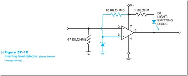
The operational amplifier is often used as a level detector or comparator. In this type of circuit, the 741 op amp will be used as an inverted amplifier to detect when one voltage becomes greater than another. Refer to the circuit shown in Figure 57–10. Notice that this circuit does not use
an above- and below-ground power supply. Instead it is connected to a power supply with a single positive and negative output. During normal operation, the noninverting input of the amplifier is connected to a zener diode. This zener diode produces a constant positive voltage at the noninverting input of the amplifier, which is used as a reference. As long as the noninverting input is more positive than the inverting input, the output of the amplifier will be high. A light-emitting diode, D1, will be used to detect a change in the polarity of the output. As long as the output of the op amp remains high, the LED will be turned off. When the output of the amplifier is high, the LED has equal voltage applied to both its anode and cathode. Since both the anode
and cathode are connected to +12 volts, there is no potential difference and therefore no current flow through the LED.
If the voltage at the inverting input should become more positive than the reference voltage applied to pin #3, the output voltage will go low. The low voltage at the output will be about +2.5 volts. The output voltage of the op amp will not go to 0 or ground in this circuit because the op amp is not connected to a voltage that is below ground. If the output voltage is to be able to go to 0 volts, pin #4 must be connected to a voltage that is below ground. When the output is low there is a potential of about 9.5 volts (12 – 2.5 = 9.5) produced across R1 and D1, which causes the LED to turn on and indicate that the state of the op amp’s output has changed from high to low.
In this type of circuit, the op amp appears to be a digital device in that the output seems to have only two states, high or low. Actually, the op amp is not a digital device. This circuit only makes it appear digital. Notice there is no negative feedback loop connected between the output and the inverting input. Therefore, the amplifier uses its open loop gain, which is about 200,000 for the 741, to amplify the voltage difference between the inverting input and the noninverting input. If the voltage applied to the inverting input should become 1 millivolt more positive than the reference voltage applied to the noninverting input, the amplifier will try to pro- duce an output that is 200 volts more negative than its high-state voltage (.001 X 200,000 = 200). The output voltage of the amplifier cannot be driven 200 volts more negative, of course, because there is only 12 volts applied to the circuit, so the output voltage simply reaches the lowest voltage it can and then goes into saturation. The op amp is not a digital device, but it can be made to act like one.
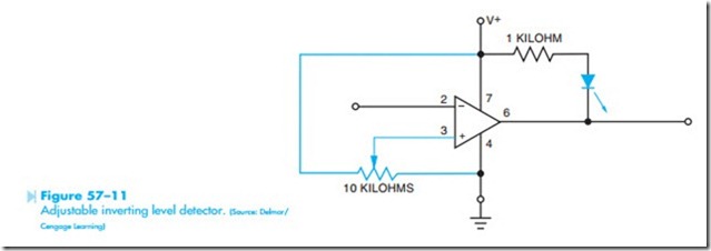
If the zener diode is replaced with a voltage divider, as shown in Figure 57–11, the reference voltage can be set to any value desired. By adjusting the variable resistor shown in Figure 57–11, the positive volt- age applied to the noninverting input can be set for any voltage value desired. For instance, if the volt- age at the noninverting input is set for 3 volts, the output of the op amp will go low when the voltage applied to the inverting input becomes greater than +3 volts. If the voltage at the noninverting input is set for 8 volts, the output voltage will go low when the voltage applied to the inverting input becomes greater than +8 volts. Notice that this circuit permits the voltage level at which the output of the op amp will change to be adjusted.
In the two circuits just described, the op amp changed from a high level to a low level when activated. There may be occasions, however, when it is desired that the output be changed from a low level to a high level. This can be accomplished by con- necting the inverting input to the reference voltage and connecting the noninverting input to the volt- age being sensed, Figure 57–12. In this circuit, the zener diode is used to provide a positive reference voltage to the inverting input. As long as the voltage at the inverting input remains more positive than the voltage at the noninverting input, the output voltage of the op amp will remain low. If the voltage applied to the noninverting input should become more positive than the reference voltage, the output of the op amp will become high.
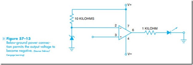
Depending on the application, this circuit could cause a small problem. As stated previously, since this circuit does not use an above- and below-ground power supply, the low output voltage of the op amp will be about +2.5 volts. This positive output voltage could cause any other devices connected to the op amp’s output to be turned on even if it should be turned off. For instance, if the LED shown in Figure 57–12 was used, it would glow dimly even when the output is in the low state. This problem can be corrected in a couple of different ways. One way would be to connect the op amp to an above- and below-ground power supply as shown in Figure 57–13.
In this circuit, the output voltage of the op amp will be negative or below ground as long as the volt- age applied to the inverting input is more positive than the voltage applied to the noninverting input. As long as the output voltage of the op amp is negative with respect to ground, the LED is reverse biased and can- not operate. When the voltage applied to the noninverting input becomes more positive than the voltage applied to the inverting input, the output of the op amp will become positive and the LED will turn on.
The second method of correcting the output voltage problem is shown in Figure 57–14. In this circuit, the op amp is connected to a power supply that has a single positive and negative output as before. A zener diode, D2, has been connected in series with the output of the op amp and the LED. The voltage value of diode D2 is greater than the output voltage of the op amp in the low state, but less than the output voltage of the op amp in its high state. For example, assume the value of the zener diode D2 is 5.1 volts. If the output voltage of the op amp in its low state is 2.5 volts, diode D2 is turned off and will not conduct. If the output volt- age becomes +12 volts when the op amp switches to its high state, the zener diode will turn on and conduct current to the LED. Notice that the zener diode D2 keeps the LED turned completely off until the op amp switches to its high state and provides enough voltage to overcome the reverse voltage drop of the zener diode.
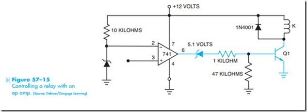
In the preceding circuits, an LED was used to indicate the output state of the amplifier. Keep in mind that the LED is used only as a detector, and
the output of the op amp could be used to control almost anything. For example, the output of the op amp can be connected to the base of a transistor as shown in Figure 57–15. The transistor can then control the coil of a relay, which could be used to control almost anything.
The Oscillator
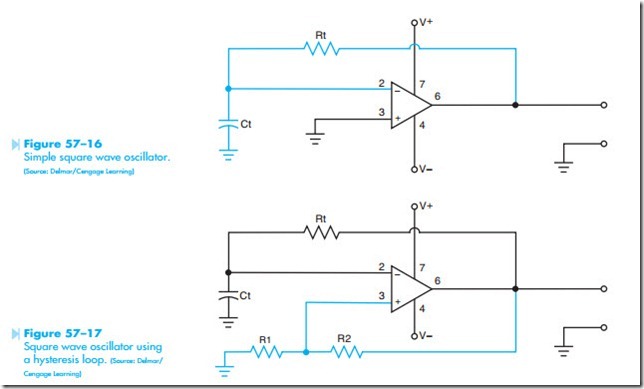
An operational amplifier can be used as an oscillator. The circuit shown in Figure 57–16 is a very simple circuit that will produce a square wave out- put. This circuit is rather impractical, however. This circuit would depend on a slight imbalance in the op amp or random circuit noise to start the oscil- lator. A slight voltage difference of a few millivolts between the two inputs is all that is needed to cause the output of the amplifier to go high or low. For example, if the inverting input becomes slightly more positive than the noninverting input, the output will go low or negative. When the output becomes negative, capacitor Ct begins to charge
through resistor Rt to the negative value of the output voltage. As soon as the voltage applied to the inverting input becomes slightly more negative than the voltage applied to the noninverting input, the output will change to a high or positive value of voltage. When the output becomes positive, capaci- tor Ct begins charging through resistor Rt toward the positive output voltage. This circuit will work quite well if the op amp has no imbalance, and if the op amp is shielded from all electrical noise. In practi- cal application, however, there is generally enough imbalance in the amplifier or enough electrical noise to send the op amp into saturation, which stops the operation of the circuit.
The Hysteresis Loop
The problem with this circuit is that a millivolt dif- ference between the two inputs is enough to drive the amplifier’s output from one state to the other. This problem can be corrected by the addition of a hysteresis loop connected to the noninverting
input as shown in Figure 57–17. Resistors R1 and R2 form a voltage divider for the noninverting input. These resistors are generally of equal value. To understand the circuit operation, assume that the inverting input is slightly more positive than the noninverting input. This causes the output voltage to go negative. Also assume that the output voltage is now negative 12 volts as compared with ground. If resistors R1 and R2 are of equal value, the non- inverting input is driven to –6 volts by the voltage divider. Capacitor Ct begins to charge through resistor Rt to the value of the output voltage. When capacitor Ct has been charged to a value slightly more negative than the -6 volts applied to the non- inverting input, the op amp’s output goes high or to +12 volts above ground. When the output of the op amp changes from -12 volts to +12 volts, the voltage applied to the noninverting input changes from -6 volts to +6 volts. Capacitor Ct now begins to charge through resistor Rt to the positive volt- age of the output. When the voltage applied to the inverting input becomes more positive than the voltage applied to the noninverting input, the output changes to a low value or -12 volts. The voltage applied to the noninverting input is driven from +6 volts to -6 volts, and capacitor Ct again begins to charge toward the negative output volt- age of the op amp. Notice that the addition of the hysteresis loop has greatly changed the operation of the circuit. The voltage differential between the two inputs is now volts instead of millivolts. The output frequency of the oscillator is determined by the values of Ct and Rt. The period of one cycle can be computed by using the formula (T = 2RC).
The Pulse Generator
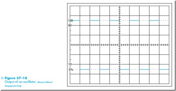
The operational amplifier can also be used as a pulse generator. The difference between an oscillator and a pulse generator is the period of time the output remains on as compared to the period of time it remains low or off. An oscillator is generally considered to produce a waveform that has posi- tive and negative pulses of equal voltage and time, Figure 57–18. Notice that the positive value of volt- age is the same as the negative value. Also notice
that both the positive and negative cycles remain turned on the same amount of time. This waveform is consistent with that which one would expect to see if an oscilloscope is connected to the output of a square wave oscillator.
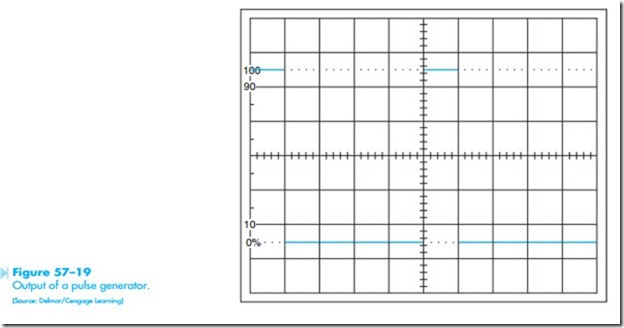
If the oscilloscope is connected to a pulse genera- tor, however, a waveform similar to the one shown in Figure 57–19 would be seen. Notice that the positive value of voltage is the same as the negative value just as it was in Figure 57–18. However, the positive pulse is of a much shorter duration than the negative pulse. The device producing this wave- form is generally considered to be a pulse generator rather than an oscillator.
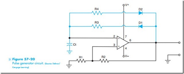
The 741 operational amplifier can eas- ily be changed from a square wave oscillator to a pulse generator. Refer to the circuit shown in Figure 57–20. This is the same basic circuit as the square wave oscillator with the addition of resistor R3 and R4, and diodes D1 and D2. This circuit permits capacitor Ct to charge at a different rate when the output is high or positive than it does when the out- put is low or negative. For instance, assume that the voltage of the op amp’s output is low or –12 volts. If the output voltage is negative, diode D1 is reverse biased and no current can flow through resistor R3. Therefore, capacitor Ct must charge through resistor R4 and diode D2, which is forward biased. When the voltage applied to the invert- ing input becomes more negative than the volt- age applied to the noninverting input, the output voltage of the op amp becomes +12 volts. When the output voltage becomes +12 volts, diode D2 is reverse biased and diode D1 is forward biased. Capacitor Ct, therefore, begins charging toward the +12 volts through resistor R3 and diode D1. Notice that the amount of time the output of the op
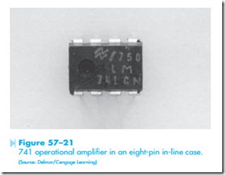
amp remains low is determined by the value of Ct and R4, and the amount of time the output remains high is determined by the value of Ct and R3. The ratio of time the output voltage is high compared to the amount of time it is low can be determined by the ratio of resistor R3 to resistor R4. A 741 opera- tional amplifier is shown in Figure 57–21.
