Signal waveforms and spectra
For many digital electronic systems, the main concerns in emission control at low frequencies are associated with power line disturbance generated by switch mode power supplies. These devices switch at a relatively high rate, in the order of 30–100 kHz, and produce a line spectrum of harmonics spreading over a wide frequency band as shown in Fig. 14.3.
Without mains filtering, the emission levels from the individual harmonics are considerably in excess of the common emission limits. Care is needed in the sourcing of these subassemblies to ensure that they are compliant with the relevant standards.
At higher frequencies, noise from digital circuits switching at very high rates (clock frequencies in excess of 100 MHz are not uncommon) couples via external cables and
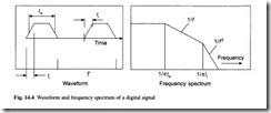
radiates in the VHF band (30–300 MHz) or it may radiate directly from circuit boards in the UHF band (300–1000 MHz). A clock oscillator has a waveform and a spectrum of the type shown in Fig. 14.4.
It can be seen that the turning points in the spectrum are (1/π) × the pulse width tw, above which frequency the spectrum decreases is inversely proportional to frequency, and (1/π ) × the rise time tr. At frequencies greater than 1/πtr the spectrum decays rapidly in inverse proportion to the square of the frequency. Thus for longer pulse dura- tions, the high-frequency content is reduced; if the rise time is slow then the content is further reduced. For good emission control, slower clock speeds and slower edges are better for EMC. This is contrary to the current trends where there are strong perform- ance demands for faster edges and higher frequency clocks.
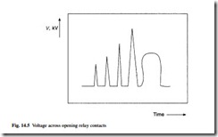
Many equipment malfunction problems in the field are caused either by transient disturbances, usually coupled onto an interface cable, or by radar transmitters if close to an airfield. The disturbance generated by a pair of relay contacts opening comprises a series of short duration impulses at high repetition rate, as illustrated in Fig. 14.5.
As the contacts separate the energy stored in the circuit inductance is released, causing a high voltage to occur across the contacts. The voltage is often sufficient to cause a discharge and a spark jumps across the gap. This is repeated until the gap is too wide. When coupled into a digital electronic circuit, the disturbance can change the state of a device and interference in the form of an unwanted operation or circuit ‘lock-up’ occurs. Control is exercised by ensuring that the receptor circuit has adequate immu- nity to this type of disturbance.
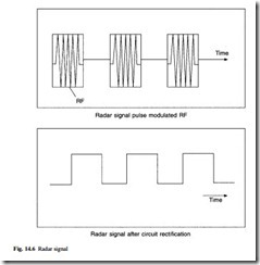
The radar transmission is one example of a modulated radio frequency signal, and this can often cause interference even in low-frequency electronic circuits. The radio frequency energy is rectified at the first semiconductor junction encountered in its propagation path through the equipment, effectively acting as a diode rectifier or demodulator. The rectified signal, an impulse wave in the case of a radar, is thus processed by the circuit electronics and interference may result if the induced signal is of sufficient amplitude, see Fig. 14.6.
Most equipment is designed and constructed to be immune to radio frequency fields of 3 V/m (or 10 V/m for industrial environments) at frequencies up to 1 GHz. Many radars operate at frequencies above 1 GHz (for example 1.2 GHz, 3 GHz and 9.5 GHz) and equipment close to an airfield may suffer interference because it is not designed
to be immune. Under these circumstances, architectural shielding is required, often comprising the use of glass with a thin metallic coating which provides adequate light transmittance and, more importantly, effective shielding at these high radio frequencies.


