Simulation Results and Discussion
In this section, simulation results of SWG structures and reflection losses are discussed. The simulation results are carried out using the OptiFDTD software package, which is based on the FDTD method developed by Optiwave Inc. [20]. This method is a powerful engineering tool for integrated and diffractive optics device simulations. Light propagation, scattering and diffraction, reflection and polarization effects can be simulated by this method. This software gives numerical solutions by using Maxwell’s equation.
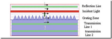
Figure 13 shows a simple schematic diagram for the simulation of triangular (or conical) shaped SWG structure of Galium Arsanide (GaAs). The incident light directly hits on top of the SWG structure (or nanostructure). A major portion of light is absorbed by the grating zone (here, these are triangular shaped nanogratings) due to the gradual change in refractive index in the grating zone, some portion of the light is reflected and the remaining portion of the light is transmitted through the GaAs substrate.
The FDTD method is used to simulate the reflection losses on the SWG structures for high efficiency GaAs solar cells. The nano-grating pitch (or period) and height of the SWG structures were varied to achieve the minimum reflection losses in GaAs solar cells. Figure 14 shows the light reflection losses spectra for several nano-grating heights (such as the heights are from 100 to 400 nm) with different pitches (or periods). The pitches or periods are: (a) 200 nm, (b) 300 nm, (c) 350 nm, (d) 400 nm, and (e) 830 nm. For this simulation, the incident light wavelength is kept constant at 830 nm. The simulated results show that with the increase in nano-grating heights the light reflection reduces and reached to the saturation of light reflection at 300 nm. The simulated results show that when the nano-grating height is *300 nm the reflection loss is minimum. It is also observed that the light reflection for 300 and 350 nm grating height is very close. This nano- grating height for light reflection is minimum and it is saturated, which is the similar tendency as reported in [10]. When the nano-grating height increases further, such as 400 nm, the light reflection is increases.
Figure 15 shows the simulated light reflection versus the nano-grating height characteristics for a triangular (conical or perfect cone) shaped nano-grating structure of GaAs, having a constant period at 830 nm. The minimum reflection loss (*2 %) was observed at 300 nm nano-grating height. However, when the nano-grating height is increased to 350 and 400 nm, then the reflection loss increases further to higher order direction. So, it indicates that the nano-grating height about 300 nm has the minimum reflection loss for the GaAs substrate.
It confirms that the nano-grating height *300 nm is the optimum nano-grating height for the minimum reflection loss of GaAs solar cells.
The Poynting theorem implemented to yield the reflection, transmission, and deflection and law of energy conservation implies
where, A is the absorption, R is the zeroth-order reflection, T is the zeroth-order transmission, and D is deflection, which includes higher order reflection and transmission. When the dimensions of the structure become comparable to or less than the wavelength of light, the number of diffraction orders is reduced. It is possible to create a structure that allows only the zero-th order to propagate. All the higher orders become evanescent.
Then, the deflection component becomes negligible (i.e., it can assume that D = 0). For this reason many researchers just use the equation as follows [25]:
From the FDTD simulation analyzer, the light transmission and reflection can be calculated directly [20]. Then, Eq. (15) is used to calculate the light absorption [20].

