Wafer switches
The familiar wafer switch still fulfils most of the requirements for signal
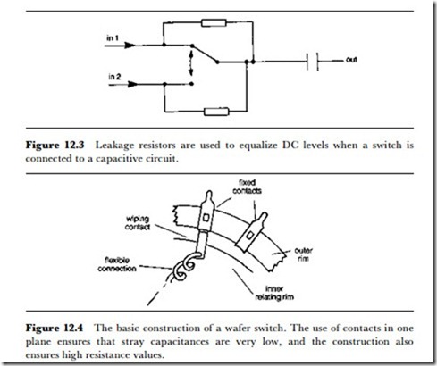
switching, particularly in low-power circuits. The layout of a wafer (Figure 12.4) ensures minimum capacitance between contacts, and also means that the contacts are cleaned by the wiping action each time the switch is used. Because of the wiping action, silver-plated contacts can be used to provide low contact resistance (and low noise) with less risk of contamination than arises when the contacts are non-wiping. The main virtue of the switch, however, is that it can be constructed to order, for example allowing wafers to be widely spaced and separated by grounded screens if this is desirable. This is possible because the rotation of the inner part of a wafer (the rotor) is controlled by a shaft that is located by a flat side, and this shaft can be cut to whatever length is needed or joined to other shafts.
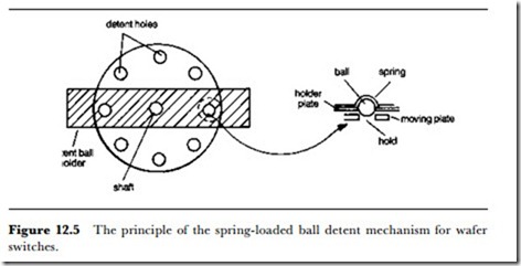
The mechanical control of the switching shaft is carried out in the section that is mounted on the panel. The switching positions are usually at 30o intervals, and the movement of the shaft is regulated by a detent mechanism (Figure 12.5) which helps to ensure that the rotating contacts are not left between fixed contacts. The detent can also assist in speeding switching times, although this is not an important factor. Careless use of a wafer switch can leave contacts isolated between detent positions, but modern mechanisms are surprisingly efficient – surprisingly, that is, because the mechanisms are comparatively simple.
The main points that distinguish the wafer switches of today from those of some 60 years ago are construction and materials. The old type of wafer switch came as a ready-made item, using wafers of laminate plastic (usually of the Bakelite family). The changes in wafer switches over the last twenty years have included the provision of switch kits that allow the user to specify the type and positioning of wafers, and of materials such as diallyl phthlate, usually glass-fibre filled, and acetals for exceptionally high insulation resistance coupled with considerable mechanical strength. The traditional form of wafer switch is still used to a very great extent, but modified wafer shapes for PCB mounting are now available. These, however, inevitably have higher capacitances between contacts than the traditional type of wafer because of the length and close spacing of the tracks to the contact pins.
;\’afers allow mainly break-before-make operation, and the standard switchings are 1-pole 12-way, 2-pole 6-way, 3-pole 4-way, 4-pole 3-way, and 6-pole 2-way. These are the standards for the traditional type of wafer switch, and not all of these switchings may be available in PCB wafers. A few make-before-break wafers are available, usually as 1-pole 12-way or 2- pole 6-way switchings. The usual length of shaft allows for the use of 6-10 wafers depending on the size and type. In addition, insulating spacers and grounding screens can be fitted between wafers, and some types allow for a dummy wafer that consists of a stator only, with contacts to allow compo- nents to be wired between wafers without recourse to the main PCB. Another useful feature of most of these wafer kits is that a miniature mains switch can be fitted at the end of a shaft to allow for mains switching in addition to signal switching. This is not desirable if the wafers handle low- level or high-impedance signals. At the switch mechanism end, a key lock can be fitted to allow the switch to be locked in positions at 60o angles.
Note that this allows only alternate contacts to be used, since the conventional wafer contact positions are at 30o.


