conduction in doped Germanium and Silicon
Pure semiconductors are mainly of theoretical inter- est. Development and research are concerned with the effects of adding impurities to pure materials. If it were not for these impurities, most semiconductors would not exist.
Pure semiconductor materials, such as germanium and silicon, support only a small number of electron-hole pairs at room temperature. This allows for conduction of very little current. To increase their conductivity, a process called doping is used.
doping is the process of adding impurities to a semiconductor material. Two types of impurities are used. The first, called pentavalent, is made of atoms with five valence electrons. Examples are arsenic and antimony. The other, called trivalent, is made of atoms with three valence electrons. Examples are indium and gallium.
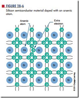
When pure semiconductor material is doped with a pentavalent material such as arsenic (As), some of the existing atoms are displaced with arsenic atoms (Figure 28-6). The arsenic atom shares four of its valence electrons with adjacent silicon atoms in a covalent bond. Its fifth electron is loosely attached to the nucleus and is easily set free.
The arsenic atom is referred to as a donor atom because it gives its extra electron away. There are many donor atoms in a semiconductor material that has been doped. This means that many free electrons are available to support current flow.
At room temperature the number of donated free electrons exceeds the number of electron-hole pairs. This means that there are more electrons than holes. The electrons are therefore called the majority carrier. The holes are minority carriers. Because the negative charge is the majority carrier, the material is called n-type material.
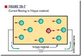
If voltage is applied to N-type material (Figure 28-7), the free electrons contributed by the donor atoms flow toward the positive terminal. Additional electrons break away from their covalent bonds and flow toward the positive terminal. These free electrons, in breaking their covalent bonds, create electron-hole pairs. The corresponding holes move toward the negative terminal.
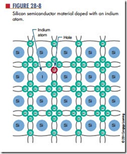
When semiconductor materials are doped with trivalent materials such as indium (I), the indium atom shares its three valence electrons with three adjacent atoms (Figure 28-8). This creates a hole in the covalent bond.
The presence of additional holes allows the electrons to drift easily from one covalent bond to the next. Because holes easily accept electrons, atoms that contribute extra holes are called acceptor atoms.
Under normal conditions, the number of holes greatly exceeds the number of electrons in such material. Therefore, the holes are the majority carrier and the electrons are the minority carrier. Because the positive charge is the majority carrier, the material is called P-type material.
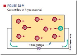
If voltage is applied to P-type material, it causes the holes to move toward the negative terminal and the electrons to move toward the positive terminal (Figure 28-9). In addition to the holes provided by the acceptor atom, holes are produced as electrons break away from their covalent bonds, creating electron-hole pairs.
N- and P-type semiconductor materials have much higher conductivity than pure semiconductor materials. This conductivity can be increased or decreased by the addition or deletion of impurities. The more heavily a semiconductor material is doped, the lower its electrical resistance.
Questions
1. Describe the process of doping a semiconductor material.
2. What are the two types of impurities used for doping?
3. What determines whether a material, when doped, is an N-type or P-type semiconductor material?
4. How does doping support current flow in a semiconductor material?
5. What determines the conductivity of a semicon- ductor material?


