Elementary Logical Processes
We have described an outline of a binary counting scale and shown how we may implement a count using it but some physical method of performing this is needed. We can represent two states, a 1 and an 0 state, by using switches since their contacts will be either open or closed and there is no half-way state. Relay contacts also share this property but there are many advantages in representing the 1 and 0 states by the polarity or existence of a voltage or a current, not least of which is the facility of handling such signals at very high speed in integrated circuitry. Manipulation of the 1 and 0 signals is
referred to as logic and, in practice, is usually implemented by simple logic circuits called gates. Digital integrated circuits comprise collections of various gates, which can number from a single gate (as in the eight input NAND gate exemplified by the 74LS30 part number) to many millions (as can be found in some microprocessors).
All logic operations can be implemented by the appropriate combination of just three operations:
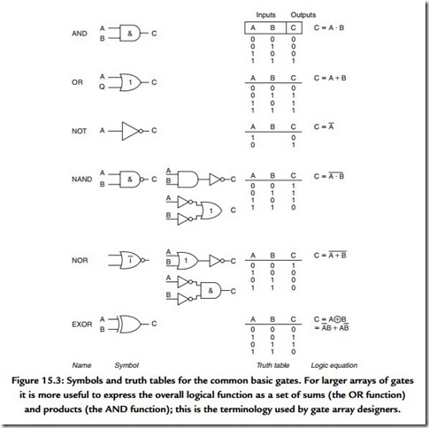
 From this primitive trio we can derive the NAND, NOR, and EXOR (exclusive-OR gate). Gates are characterized by the relationship of their output to combinations of their inputs (Figure 15.3). Note how the NAND (literally negated AND gate) performs the same logical function as OR gate fed with inverted signals and, similarly, note the equivalent duality in the NOR function. This particular set of dualities is known as De Morgan’s theorem.
Practical logic systems are formed by grouping many gates together and naturally there are formal tools available to help with the design, the most simple and common of which is known as Boolean algebra. This is an algebra that allows logic problems to be expressed in symbolic terms. These can then be manipulated and the resulting expression can be directly interpreted as a logic circuit diagram. Boolean expressions cope best with
logic that has no timing or memory associated with it: for such systems other techniques, such as state machine analysis, are better used instead.
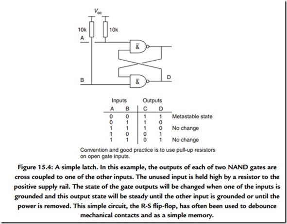
The simplest arrangement of gates that exhibit memory, at least while power is still applied, is the cross-coupled NAND (or NOR) gate (Figure 15.4). More complex
arrangements produce the wide range of flip-flop (FF) gates, including the set–reset latch, the D-type FF, which is edge triggered by a clock pulse, the JK FF and a wide range of counters (or dividers), and shift registers (Figure 15.5). These circuit elements and their derivatives find their way into the circuitry of digital signal handling for a wide variety of reasons. Early digital circuitry was based around standardized logic chips, but it is much more common nowadays to use application-specific ICs.

